EP0200359A2 - A wide band inductive transdermal power and data link - Google Patents
A wide band inductive transdermal power and data link Download PDFInfo
- Publication number
- EP0200359A2 EP0200359A2 EP86302272A EP86302272A EP0200359A2 EP 0200359 A2 EP0200359 A2 EP 0200359A2 EP 86302272 A EP86302272 A EP 86302272A EP 86302272 A EP86302272 A EP 86302272A EP 0200359 A2 EP0200359 A2 EP 0200359A2
- Authority
- EP
- European Patent Office
- Prior art keywords
- coil
- link
- coils
- coupling
- gain
- Prior art date
- Legal status (The legal status is an assumption and is not a legal conclusion. Google has not performed a legal analysis and makes no representation as to the accuracy of the status listed.)
- Granted
Links
Images
Classifications
-
- A—HUMAN NECESSITIES
- A61—MEDICAL OR VETERINARY SCIENCE; HYGIENE
- A61N—ELECTROTHERAPY; MAGNETOTHERAPY; RADIATION THERAPY; ULTRASOUND THERAPY
- A61N1/00—Electrotherapy; Circuits therefor
- A61N1/18—Applying electric currents by contact electrodes
- A61N1/32—Applying electric currents by contact electrodes alternating or intermittent currents
- A61N1/36—Applying electric currents by contact electrodes alternating or intermittent currents for stimulation
- A61N1/372—Arrangements in connection with the implantation of stimulators
- A61N1/37211—Means for communicating with stimulators
- A61N1/37217—Means for communicating with stimulators characterised by the communication link, e.g. acoustic or tactile
- A61N1/37223—Circuits for electromagnetic coupling
-
- Y—GENERAL TAGGING OF NEW TECHNOLOGICAL DEVELOPMENTS; GENERAL TAGGING OF CROSS-SECTIONAL TECHNOLOGIES SPANNING OVER SEVERAL SECTIONS OF THE IPC; TECHNICAL SUBJECTS COVERED BY FORMER USPC CROSS-REFERENCE ART COLLECTIONS [XRACs] AND DIGESTS
- Y10—TECHNICAL SUBJECTS COVERED BY FORMER USPC
- Y10S—TECHNICAL SUBJECTS COVERED BY FORMER USPC CROSS-REFERENCE ART COLLECTIONS [XRACs] AND DIGESTS
- Y10S128/00—Surgery
- Y10S128/903—Radio telemetry
Definitions
- the present invention is directed generally to the field of medical electronics, and more particularly to a method and apparatus for conveying power and data through the skin of a subject without breaking the skin.
- an inductive link has neither of these limitations since it leaves the skin intact and can draw from outside power source.
- an inductive link is usually composed of two pancake shaped coils, one implanted in the body and one outside the body. These coils form a transformer through which energy can be sent.
- Inductive links are already used to deliver power and information into implanted stimulators. Examples of this can be found in the Ph.D. Dissertation of M. Soma, "Design and Fabrication of an Implantable Multi-channel Neutral Stimulator" Ph.D. Dissertion June, 1980; the Ph.D. Dissertion of T.
- Yet another objective of the present invention is to provide an inductive link which has a relatively wide bandwidth.
- Efficiency is one of the major problems to be attacked in designing such coupling. systems. Efficiency is a problem because the freedom of the implanted person is limited by the portability of the transmitter power source. If the transdermal link is inefficient, an implant of even modest power demand may require a large amount of power to the transmitter. If the system requires an excessive amount of power, the individual must carry a large battery pack. For example, the systems described in the above-referenced Ph.D. theses required a battery pack about the size of a brick which needed recharging every eight hours.
- Inductive links have been inefficient because designs to compensate for coil misalignment have been inefficient.
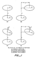
- the coils can move relative to one another as shown in Figure 1. As they move, their gain (voltage gain, current gain, transconductance gain, or transimpedance gain, depending on the input and output circuitry) changes, since their coupling depends on their relative positions. Many applications require a stable intemal power supply, and therefore, must regulate the output of the receiver coil.
- the earlier links also had another problem, i.e., poor bandwidth. These links were usually single tuned (transmitter coil only) or double tuned (both coils) to the carrier frequency so that they could be driven by a semi-passive RF transmitter (Class C, for example) for higher efficiency. Semi-passive transmitters need a high Q tuned circuit to operate efficiently. Unfortunately, the higher the Q, the smaller the band width. The previous Stanford stimulators used a separate ultrasonic data link to obtain a wide band data path, but that link proved much less tolerant to misalignment than the inductive link, and unreliable in use due to acoustic impedance mismatches. Clearly,an efficient wide band power and data link would solve some difficult problems.
- the new approach described in the present invention utilizes a pair of coils, one beneath the skin and one outside the skin, each connected to a capacitor.
- the values of the capacitor and coil inductance are selected to provide a stagger-tuned link. That is, the values of the components are selected to place the pole of one filter above the operating frequency, and the pole of the other filter below the operating frequency of the link.
- the poles will move as the coupling coefficient changes, desensitizing the link to the coupling so that the coils can be misaligned in any manner with little effect on the output.
- the present invention includes a number of approaches which differ from obvious uses of stagger tuning or any prior art approaches.
- the problem is that when the coils move, the coupling coefficient changes and so does the ratio of input to output.
- the present invention applies stagger tuning to desensitize the link going into the coupling coefficient rather than broaden the band width as is normally done in stagger-tuned filters.
- the gain is stabilized due to an approach which takes into account and relies on the interaction of two components; typically, gain is stablized by isolating components from affecting one another.
- a fully active driver or class D amplifier is preferably utilized to effectively drive the link with a square wave signal.
- This signal can be modulated to convey data information to the implanted receiver coil beneath the skin.
- the "Voltage Driven:Voltage Out” link of Figure 2A will illustrate the approach of the present invention to gain control.
- the voltage gain across an untuned or singly tuned two-coil system varies linearly with the coupling coefficient (assuming the load resistance is large compared to the coil reactance), so if the coupling increases by a factor of three, it will cause the voltage gain to triple.
- This lax gain control is generally unacceptable because it usually wastes most of the received power in the voltage regulation.
- This circuit reduces the coupling dependent gain variations by tuning the coils to two different frequencies; one above and one below the operating frequency. If these coils' resonances are placed optimally, their effective poles will shift as the mutual coupling of the coils changes. The gain will be compensated as a result.
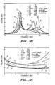
- Figure 3 is a plot of the voltage gain versus frequency and coupling .for a link that was designed to operate at 20 MHz.
- the link is stagger-tuned, i.e., the component values are selected as shown so that one pole is placed above the operating frequency (20 MHz) and one pole below.
- the poles move as the coupling coefficient changes. If they are placed properly, their positions move to compensate for the changing coupling. To illustrate, in Figure 3 as the coupling increases, the poles move away from the operating frequency.
- the link needs a transmitter that can efficiently handle a variable load impedance while maintaining a constant driving voltage or current.
- Semi-passive drivers such as class C or class E, are not practical because they lose efficiency if the load impedance is not resonant at the operating frequency, a fundamental incompatibility with stagger tuning.
- a class D transmitter can drive these loads efficiently, and can supply a constant driving source so that the link output voltage, or current, remains stable.
- a class D transmitter can drive these loads efficiently, because it can supply a constant source which is independent of the load. It simply switches the input of the link between the two terminals of the power supply. Reactive loads and load variations, due to changing coupling, should not affect its output level.
- This driver also has a theoretical maximum efficiency of 100%, meaning that its efficiency is not bounded by a sub-optimum theoretical limit, an advantage in any design.
- the driver's loss is proportional to the ratio of the voltage dropped across its switches to the supply voltage. It is fairly simple to make this ratio quite small, and in practice, the design tends to become more efficient as the output power level is raised, In fact, the efficiency improves when it is needed most, when the transmitter is delivering the maximum power.
- the class D driver therefore, meets the requirements for driving the stagger tuned link; it can efficiently drive a variable load with a stable source.
- a class D driver has another advantage due to its square wave output.
- the Fourier Series of a square wave has a fundamental sine wave whose amplitude is 4/.w times the amplitude of the square wave.
- the stagger tuned link passes the fundamental and attenuates the harmonics, meaning that the class D driver provides the added advantage of another 27% increase in gain.
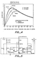
- Figure 4 shows the theoretical and experimental gain versus coupling for the 20 MHz link described above. It has a correction factor of 0.745 which means that the theoretical gain is multiplied by 0.745 to match the experimental results. The difference between theory and practice comes from operating the coils near their self-resonant frequencies.
- the parasitic capacitance of the transmitter coil acts with the tuning capacitance to form a voltage divider between the transmitter and the inductor. It lowers the amount of voltage reaching the tuned circuit. In this example, the additional square wave gain (27%) was used to replenish the gain lost to the self resonance.
- a typical class D driver usable with the coils described above is shown in Figure 5.
- This procedure initially determines whether a design is feasible. If so, then it uses an iterative process to meet the design goals.
- the procedure begins by specifying the type of link, coupling range, load range, and operating frequency. These choices may be limited by size constraints, FCC regulations, or power requirements.
- the equation below is an approximation which applies to all of the link combinations. It gives the ratio of the magnitude of the minimum gain to the maximum gain (G) in terms of a ratio of the minimum and maximum coupling coefficients - ( Xmin and Xmax ). Note that O ⁇ x min ⁇ x max ⁇ and O ⁇ G ⁇ 1.
- the coupling range (x min and x max ) is usually found experimentally. If the gain variation is too large (G is too small),. then the coupling range needs to be reduced (preferably by raising the minimum value of coupling which has the added advantages of lowering the transmitter coil losses by reducing the transmitter current, and also improving the load insensitivity of the gain by lowering the link output impedance).
- One possible solution is to use larger coil diameters. A larger diameter will reduce the coupling range as long as the alignment tolerance is held constant.
- Another solution is to use a ferrite backing on either or both coils. The ferrite will compress the magnetic field around the coils and raise their mutual coupling.
- the procedure tends to be iterative.
- the minimum inductance of each of the two coils is chosen.
- the receiver coil inductance must provide a reasonable Q (for example, greater than 10) for the loaded receiver tank circuit. If the Q is too low, the output voltage will be sensitive to changes in the load. Also, to maintain a reasonable overall efficiency, the transmitter coil inductance should provide a large enough input impedance so that the transmitter will not have to supply an excessive current into the link (generally, raising the transmitter coil's inductance raises the link's input impedance).
- the next step is to set the minimum gain and reduce the gain variation over a band of frequencies.
- a ratio of receiver resonance to the operating frequency ( ⁇ r / ⁇ ) is chosen. (Remember, if the link is driven by a class D transmitter, ( ⁇ r / ⁇ ) should be chosen so that the input impedance looks inductive, which allows the transmitter to provide efficient switching.) This ratio along with the resistances, coupling range and coil inductances, fixes the ratio of the transmitter resonance to the operating frequency ( ⁇ t / ⁇ ).
- the equations which specify ⁇ t / ⁇ are different for each type of link and are given below.
- plots are made ' of the gain versus frequency for the six combinations of minimum and maximum load (R min ,R max ); and minimum, optimum, and maximum values of coupling (k min , K opt ,K max ).
- the required gain is obtained by varying the turns ratio (inductance of the coils and adjusting ⁇ r / ⁇ . For example, if the gain is too small, then the turns ratio should be changed or ⁇ r / ⁇ moved closure to unity. If the gain variation, due to loading, is too large over the frequency band, then the receiver coil Q should be increased. If the spread is lop-sided (more variation on one side of the band than on the other), then ⁇ r / ⁇ needs to be slightly adjusted until the gain is acceptably uniform about the operating frequency.
- link gain equation There are four combinations of link gain; voltage gain, current gain, transconductance gain, and transimpedance gain.
- the link gain equation for all four combinations has the form where k is the coupling coefficient (O ⁇ x ⁇ 1), and A, B, C, D, and E are variables dependent on the link combination.
- the ratio of the minimum gain to the maximum gain is the ratio of the minimum gain to the maximum gain.
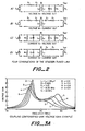
- Figure 2A is a circuit diagram of a stagger-tuned link which is driven by a voltage source and whose output appears as a voltage source. This arrangement is the type used by a preferred embodiment. For this circuit the general parameters are
- the ratio of minimum to maximum voltage gain is approximately 0.90, which is well within the goal of 0.5.
- two identical coils, with ferrite backings for high coupling are chosen. They are 1.96 ⁇ h with a series resistance of 5.8 ⁇ at 20 MHz. These numbers give a transmitter tank Q of about 40 and a receiver tank Q, including the 1x ⁇ load, of about four.
- Figure 3B is a plot of the gain versus frequency for the six combinations of coupling and load, using the equations in the appendix for a "voltage driven:voltage out" link.
- Figure 3C is an expanded view of the gain around the operating frequency (20 MHz).
- the maximum gain deviation occurs at the high end of the frequency range (21 MHz).
- the ratio of minimum to maximum gain is 0.7 which exceeds the design goal of 0.5.
- the minimum gain is about 1.9 which is only 5% below the goal of 2, well within the tolerances of most components, and probably acceptable.
- the output impedance of the link (equivalent to about 800 ohms) is significant compared to the load, so the output voltage is somewhat load sensitive.
- Two ways of reducing the output impedance are: one, raise the coupling coefficient (use ferrite backings and larger coil diameters); and two, make sure that the Q of the loaded receiver coil is reasonably high (adjust the receiver coil inductance).
- FIG. 5 shows a preferred embodiment of a transmitter design used to drive the link.
- This circuit is a class D FM voltage driver with several features for portable, efficient operation. Its frequency is fairly insensitive to changes in the power supply voltage, so that it can operate from transistor radio batteries without regulation. Its frequency deviation is controlled by a CMOS compatible input which interfaces easily to portable digital logic. It also uses core drivers in the output stage to rapidly and efficiently switch the high output currents.
- the stagger-tuned link in this example, has a minimum input impedance of about 47H, a fairly small load for the transmitter to drive.
- AM efficiency of 35% allows the link to operate for a full day (16 hours) on two nine volt transistor radio batteries. This efficiency provides a major reduction in power consumption and battery size over previous Stanford stimulators (a worst case power consumption of 140mW intead of 400mW, and two nine volt batteries instead of a brick-sized battery pack).
- the link receives its power from an RF carrier sent across the inductive link, and extracts its data from a frequency-modulation (FM) of this carrier.
- FM frequency-modulation
- This approach decouples the information from the output voltage, again keeping the output voltage fairly constant for the sake of efficiency.
- FM requires a wider bandwidth than that needed for just the data.
- This link provides that additional bandwidth.
- This link is still capable of delivering a base-band data rate of one megabit per second. This data rate is very high for a neural stimulator.
- the band-width limiting element of this system was not the link, but the FM receiver (due to transistors with only a 20 MHz beta cutoff frequency).
- the stagger-tuned link can provide both a large bandwidth and a high efficiency; two characteristics which were mutually exclusive in previous links.
- Inductive links provide a safe means of delivering both power and data into devices implanted in the body. With the appropriate applications of stagger tuning, these links can now provide a high efficiency by taking advantage of a coupling desensitized link gain. They can also supply a large bandwidth without adversely effecting their efficiency. This technique is successful in neural stimulators and can easily be applied to many other applications requiring coupling insensitivity.
Abstract
Description
- The present invention is directed generally to the field of medical electronics, and more particularly to a method and apparatus for conveying power and data through the skin of a subject without breaking the skin.
- With the increase in use of implanted electronic devices beneath human skin, it has been increasingly desirable to be able to convey power and/or data to the implanted device without puncturing the skin. A typical approach previously followed was to use a percutaneous plug which could deliver power, but must break the skin to reach the stimulator. Breaching the skin provides a potential path for infection to enter, risking the safety of the individual as well as the implant. Another alternative is to implant a battery. Unfortunately, many applications require more amp hours than a battery can provide without frequent reimplantation.
- The use of an inductive link has neither of these limitations since it leaves the skin intact and can draw from outside power source. For medical applications, an inductive link is usually composed of two pancake shaped coils, one implanted in the body and one outside the body. These coils form a transformer through which energy can be sent. Inductive links are already used to deliver power and information into implanted stimulators. Examples of this can be found in the Ph.D. Dissertation of M. Soma, "Design and Fabrication of an Implantable Multi-channel Neutral Stimulator" Ph.D. Dissertion June, 1980; the Ph.D. Dissertion of T. Gheewala, "A CMOS Implantable Auditory Prosthesis Using Integrated Circuit Technology," Stanford University, March 1976, and the article by E.S. Hochmair, IEEE Transactions on Biomedical Engineering, Vol. BME-31, No.2, pp.177-186, February 1984, entitled, "System Optimization for Improved Accuracy in Transcutaneous Signal and Power Transmission."
- However, inductive links as considered in these prior efforts have their own set of difficulties. In the past, these links have had problems providing efficiency, bandwidth, and insensitivity to misalignment.
- It is an objective of the present invention to provide a new and improved inductive link.
- It is another objective of this invention to provide such a link whose gain is relatively insensitive to coupling variations between the coils which occur with relative movement between the coils.
- Yet another objective of the present invention is to provide an inductive link which has a relatively wide bandwidth.
- Efficiency is one of the major problems to be attacked in designing such coupling. systems. Efficiency is a problem because the freedom of the implanted person is limited by the portability of the transmitter power source. If the transdermal link is inefficient, an implant of even modest power demand may require a large amount of power to the transmitter. If the system requires an excessive amount of power, the individual must carry a large battery pack. For example, the systems described in the above-referenced Ph.D. theses required a battery pack about the size of a brick which needed recharging every eight hours.
- Therefore, it is an objective of the present invention to provide a system which is small and efficient enough for a person to wear freely and use in everyday activities.
- Inductive links have been inefficient because designs to compensate for coil misalignment have been inefficient. The coils can move relative to one another as shown in Figure 1. As they move, their gain (voltage gain, current gain, transconductance gain, or transimpedance gain, depending on the input and output circuitry) changes, since their coupling depends on their relative positions. Many applications require a stable intemal power supply, and therefore, must regulate the output of the receiver coil.
- If the gain variation is too large, then most of the received power is not used in the stimulator, but wasted in the voltage regulator coupled to the receiving coil.
- The most commonly used approach to solving this problem, called the geometric approach, sacrifices the coupling magnitude in exchange for reduction in the coupling variation. It uses an external coil which is larger than the implanted coil. As long as the small coil remains within the perimeter of the larger coil, both coils will share roughly the same number of flux lines, and the coupling will remain fairly constant. The coils can move laterally and even tilt somewhat with only a minor effect on their gain. This approach is adopted in one or more of the above references.
- Unfortunately, in addition to being inefficient, the geometric approach is still sensitive to changes in coil separation; for a small separation (near field), the coupling drops proportionally with separation. If the coil separation doubles, then the gain is cut in half, This approach, therefore, only partially desensitizes the link gain to the coil's position.
- Secondly, in exchange for partially controlling the gain, the geometric approach sacrifices the magnitude of the coupling, which raises the losses in the primary coil. Since these coils share fewer flux lines than two equally sized coils, their typical coupling coefficient is lower than their equally sized counterparts. In fact, their coupling is much lower since their shared area diminishes as the square of the lateral misalignment tolerance, i.e., shared area=»(Iarger radius-alignment tolerance)2. Lower coupling requires a higher current in the primary coil to provide the same output from the receiver coil; and higher current wastes more power due to the 12R losses of the transmitter coil.
- The earlier links also had another problem, i.e., poor bandwidth. These links were usually single tuned (transmitter coil only) or double tuned (both coils) to the carrier frequency so that they could be driven by a semi-passive RF transmitter (Class C, for example) for higher efficiency. Semi-passive transmitters need a high Q tuned circuit to operate efficiently. Unfortunately, the higher the Q, the smaller the band width. The previous Stanford stimulators used a separate ultrasonic data link to obtain a wide band data path, but that link proved much less tolerant to misalignment than the inductive link, and unreliable in use due to acoustic impedance mismatches. Clearly,an efficient wide band power and data link would solve some difficult problems.
- In summary, the new approach described in the present invention utilizes a pair of coils, one beneath the skin and one outside the skin, each connected to a capacitor. The values of the capacitor and coil inductance are selected to provide a stagger-tuned link. That is, the values of the components are selected to place the pole of one filter above the operating frequency, and the pole of the other filter below the operating frequency of the link. The poles will move as the coupling coefficient changes, desensitizing the link to the coupling so that the coils can be misaligned in any manner with little effect on the output.
- The present invention includes a number of approaches which differ from obvious uses of stagger tuning or any prior art approaches. The problem is that when the coils move, the coupling coefficient changes and so does the ratio of input to output. The present invention applies stagger tuning to desensitize the link going into the coupling coefficient rather than broaden the band width as is normally done in stagger-tuned filters.
- Second, the gain is stabilized due to an approach which takes into account and relies on the interaction of two components; typically, gain is stablized by isolating components from affecting one another.
- In a further departure from the approaches of the prior art, a fully active driver or class D amplifier is preferably utilized to effectively drive the link with a square wave signal. This signal can be modulated to convey data information to the implanted receiver coil beneath the skin.
- Other advantages of the present invention will become apparent from the following detailed disclosure given with reference to the accompanying drawings wherein:
- Figures 2A through 2D show the four possible combinations of stagger-tuned links.
- Figure 3 illustrates the effective result of a coupling compensated link voltage device using the circuit combination shown in Figure 2A;
- Figure 4 is a second graph illustrating the effective relationship of gain versus coupling and load impedance at a given operating frequency of 20 MHz, and
- Figure 5 is a detailed schematic of a Class D transmitter useful in driving the link of the - present invention.
- The "Voltage Driven:Voltage Out" link of Figure 2A will illustrate the approach of the present invention to gain control. The voltage gain across an untuned or singly tuned two-coil system varies linearly with the coupling coefficient (assuming the load resistance is large compared to the coil reactance), so if the coupling increases by a factor of three, it will cause the voltage gain to triple. This lax gain control is generally unacceptable because it usually wastes most of the received power in the voltage regulation.
- Figure 2A is a schematic of the transmitter and receiver elements of an inductive link (Lt and Lr), the tuning elements (ωr=1/√LrCr and ωt=1/√LtCt, the transmitter loss and receiver load elements (Rt and Rr ) and the transmitter source and receiver voltages. This circuit reduces the coupling dependent gain variations by tuning the coils to two different frequencies; one above and one below the operating frequency. If these coils' resonances are placed optimally, their effective poles will shift as the mutual coupling of the coils changes. The gain will be compensated as a result.
- The "voltage driven:voltage out" link will help illustrate the new approach to gain control. Figure 3 is a plot of the voltage gain versus frequency and coupling .for a link that was designed to operate at 20 MHz. The numbers on the curves represent the values of coupling coefficient; 2 means x=0.2, 3 means x=0.3, and so on. The link is stagger-tuned, i.e., the component values are selected as shown so that one pole is placed above the operating frequency (20 MHz) and one pole below. The poles move as the coupling coefficient changes. If they are placed properly, their positions move to compensate for the changing coupling. To illustrate, in Figure 3 as the coupling increases, the poles move away from the operating frequency. Increased coupling would normally raise the gain at 20 MHz, but the higher coupling has moved the poles away from the 20 MHz operating frequency, therefore lowering the gain at the operating frequency. The net result, for this example, is that even though the coupling coefficient changes by 250%, the gain changes by less than ±10%.
- Since this approach is based on coupling, not geometry, it not only corrects for lateral displacement and tilt, as did the prior art geometric approach, but it also handles coil separation, which the geometric solution did not.
- Also notice that the gain changes smoothly around the operating frequency (20 MHz), giving a stable gain over a relatively large frequency band. Classically, stagger tuning has been used to increase the bandwidth of a system without excessively loading the tuned circuits. As the example of Figure 3 shows, the new approach to gain control has carried over the attractive feature of a wide bandwidth. For many applications, the additional bandwidth can simplify the design. For example, power and data links are combined into one inductive link by sending power on the carrier and the data by frequency-modulating (FM) the carrier as discussed in the application of Galbraith, et al. - (Attorney's Docket No. A-41833) filed concurrently herewith and entitled,- An Eight Channel Implantable Neural Stimulator," incorporated herein by reference.
- This example has clearly demonstrated a wind link gain which is coupling-insensitive. With these capabilities, the power lost across the internal voltage regulators of an implanted stimulator can be reduced by taking advantage of the stable gain. By using equal sized coils, instead of the mismatched coil sizes of the geometric approach, the average coupling can be improved which lowers the transmitter coil 12R losses. The coupling-compensated link not only allows improved efficiency, but it also provides a large bandwidth, something that the previous approaches have sacrificed for efficiency.
- To take advantage of the efficiency afforded by the stagger-tuned link's stable gain, the link needs a transmitter that can efficiently handle a variable load impedance while maintaining a constant driving voltage or current. Semi-passive drivers, such as class C or class E, are not practical because they lose efficiency if the load impedance is not resonant at the operating frequency, a fundamental incompatibility with stagger tuning. A class D transmitter, on the other hand, can drive these loads efficiently, and can supply a constant driving source so that the link output voltage, or current, remains stable.
- A class D transmitter, on the other hand, can drive these loads efficiently, because it can supply a constant source which is independent of the load. It simply switches the input of the link between the two terminals of the power supply. Reactive loads and load variations, due to changing coupling, should not affect its output level.
- This driver also has a theoretical maximum efficiency of 100%, meaning that its efficiency is not bounded by a sub-optimum theoretical limit, an advantage in any design. The driver's loss is proportional to the ratio of the voltage dropped across its switches to the supply voltage. It is fairly simple to make this ratio quite small, and in practice, the design tends to become more efficient as the output power level is raised, In fact, the efficiency improves when it is needed most, when the transmitter is delivering the maximum power. The class D driver, therefore, meets the requirements for driving the stagger tuned link; it can efficiently drive a variable load with a stable source.
- A class D driver has another advantage due to its square wave output. The Fourier Series of a square wave has a fundamental sine wave whose amplitude is 4/.w times the amplitude of the square wave. The stagger tuned link passes the fundamental and attenuates the harmonics, meaning that the class D driver provides the added advantage of another 27% increase in gain. Other design considerations may trade off this additional gain to further advantage. For example, Figure 4 shows the theoretical and experimental gain versus coupling for the 20 MHz link described above. It has a correction factor of 0.745 which means that the theoretical gain is multiplied by 0.745 to match the experimental results. The difference between theory and practice comes from operating the coils near their self-resonant frequencies. The parasitic capacitance of the transmitter coil acts with the tuning capacitance to form a voltage divider between the transmitter and the inductor. It lowers the amount of voltage reaching the tuned circuit. In this example, the additional square wave gain (27%) was used to replenish the gain lost to the self resonance. A typical class D driver usable with the coils described above is shown in Figure 5.
- Now that the concept behind the gain control and its drive requirements have been described and examples shown, it is appropriate to discuss a design procedure, including some of the design tradeoffs.
- The following procedure was used to create a stagger tuned power and data link; a "voltage driven:voltage out" link. The goals for this procedure were:
- 1) to minimize the variation in output voltage, due to changing load and coupling, over a band of frequencies;
- 2) to keep a reasonably high input impedance so a transmitter would not need to supply excessively large driving currents;
- 3) to make the input impedance inductive so that a class D voltage driver would switch cleanly; and
- 4) to exceed a minimum required voltage gain.
- This procedure initially determines whether a design is feasible. If so, then it uses an iterative process to meet the design goals.
- The procedure begins by specifying the type of link, coupling range, load range, and operating frequency. These choices may be limited by size constraints, FCC regulations, or power requirements. The equation below is an approximation which applies to all of the link combinations. It gives the ratio of the magnitude of the minimum gain to the maximum gain (G) in terms of a ratio of the minimum and maximum coupling coefficients - (Xmin and Xmax ). Note that O≦xmin≦xmax≦ and O≦G≦1.

- The coupling range (xmin and xmax) is usually found experimentally. If the gain variation is too large (G is too small),. then the coupling range needs to be reduced (preferably by raising the minimum value of coupling which has the added advantages of lowering the transmitter coil losses by reducing the transmitter current, and also improving the load insensitivity of the gain by lowering the link output impedance). One possible solution is to use larger coil diameters. A larger diameter will reduce the coupling range as long as the alignment tolerance is held constant. Another solution is to use a ferrite backing on either or both coils. The ferrite will compress the magnetic field around the coils and raise their mutual coupling.
- Since the gain is still somewhat dependent on coupling, it is necessary to find the values of coupling which produce the minimum and maximum values of gain. The minimum gain occurs, by design, at the minimum and maximum values of coupling (kmm and kmax). The maximum gain occurs at the optimum value of coupling given by equation Kopt = KminKmax
- From here on, the procedure tends to be iterative. Next, the minimum inductance of each of the two coils is chosen. The receiver coil inductance must provide a reasonable Q (for example, greater than 10) for the loaded receiver tank circuit. If the Q is too low, the output voltage will be sensitive to changes in the load. Also, to maintain a reasonable overall efficiency, the transmitter coil inductance should provide a large enough input impedance so that the transmitter will not have to supply an excessive current into the link (generally, raising the transmitter coil's inductance raises the link's input impedance).
- The next step is to set the minimum gain and reduce the gain variation over a band of frequencies. A ratio of receiver resonance to the operating frequency (ωr/ω) is chosen. (Remember, if the link is driven by a class D transmitter, (ωr/ω) should be chosen so that the input impedance looks inductive, which allows the transmitter to provide efficient switching.) This ratio along with the resistances, coupling range and coil inductances, fixes the ratio of the transmitter resonance to the operating frequency (ωt/ω). The equations which specify ωt/ω are different for each type of link and are given below.
- Next, plots are made 'of the gain versus frequency for the six combinations of minimum and maximum load (Rmin ,Rmax); and minimum, optimum, and maximum values of coupling (kmin, Kopt,Kmax). The required gain is obtained by varying the turns ratio (inductance of the coils and adjusting ωr/ω. For example, if the gain is too small, then the turns ratio should be changed or ωr/ω moved closure to unity. If the gain variation, due to loading, is too large over the frequency band, then the receiver coil Q should be increased. If the spread is lop-sided (more variation on one side of the band than on the other), then ωr/ω needs to be slightly adjusted until the gain is acceptably uniform about the operating frequency.
- There are four combinations of link gain; voltage gain, current gain, transconductance gain, and transimpedance gain. The link gain equation for all four combinations has the form


- Summarizing for the general section: the minimum gain occurs at kmm and kmax, while the maximum gain occurs at


- The ratio of the minimum gain to the maximum gain is

- Therefore, the amount of gain variation (G) and the coupling values where the minimum and maximum gains occur (fmin=f(kmin)=f(kmax), and fmax=f-(kopt)) are known by simply specifying the coupling range.
- Figure 2A is a circuit diagram of a stagger-tuned link which is driven by a voltage source and whose output appears as a voltage source. This arrangement is the type used by a preferred embodiment. For this circuit the general parameters are
-


- Note that x4 opt = Z/X = (C2+E2)/(B2+D2). So substituting and simplifying give

- Solving for the ratio of the operating frequency to the transmitte resonance ω2/ω2b and simplifying gives


- Therefore, given the minimum and maximum coupling coefficient, the coil Q's, the operating frequency, and the resonant frequency of the receiver, equation gives the transmitter resonance that minimizes the sensitivity of the gain to the coupling variations. The other three possible stagger-tuned links shown in Fig. 3 follow an equivalent approach.
- Further details of an exemplary embodiment will be given below.
- * link type: "voltage driven : voltage out"
- * coupling range: 0.2≦x≦0.5
- * load range: 1xΩ≦R≦3xΩ
- * operating frequency: 20 MHz
- * frequency range 19MHz≦f≦21 MHz
- * transmitter type: class D voltage source
- * acceptable gain variation across the bandwidth, including the load variation: 0.5 drop from the maximum
- minimum gain: ≅2.0
- The ratio of minimum to maximum voltage gain is approximately 0.90, which is well within the goal of 0.5. Next, two identical coils, with ferrite backings for high coupling, are chosen. They are 1.96µh with a series resistance of 5.8Ω at 20 MHz. These numbers give a transmitter tank Q of about 40 and a receiver tank Q, including the 1xΩ load, of about four.
- Next, ωr/ω is chosen greater than one so that the input appears inductive for the class D transmitter. Let ωr/ω =1.1.
- Figure 3B is a plot of the gain versus frequency for the six combinations of coupling and load, using the equations in the appendix for a "voltage driven:voltage out" link.
- Figure 3C is an expanded view of the gain around the operating frequency (20 MHz). The maximum gain deviation occurs at the high end of the frequency range (21 MHz). The ratio of minimum to maximum gain is 0.7 which exceeds the design goal of 0.5. The minimum gain is about 1.9 which is only 5% below the goal of 2, well within the tolerances of most components, and probably acceptable.
- Remember that the receiver Q was rather low, only 4. The dependence of the output voltage on the load is the result of a voltage division between the link output impedance and the effective load impedance. If the link impedance is significant compared to the load, then the output voltage will be load dependent. The curves labeled 1 and 4 on Figure 3C illustrate this point. These curves represent the gain for the minimum and maximum loads at the lowest value of coupling. This link has its highest output impedance when the coils are coupling the least. Over the design band (19 MHz-21 MHz), the largest gain spread occurs at 21 MHz and is bounded by
curves - As mentioned before, this link places some requirements on the driver. Figure 5 shows a preferred embodiment of a transmitter design used to drive the link. This circuit is a class D FM voltage driver with several features for portable, efficient operation. Its frequency is fairly insensitive to changes in the power supply voltage, so that it can operate from transistor radio batteries without regulation. Its frequency deviation is controlled by a CMOS compatible input which interfaces easily to portable digital logic. It also uses core drivers in the output stage to rapidly and efficiently switch the high output currents.
- The stagger-tuned link, in this example, has a minimum input impedance of about 47H, a fairly small load for the transmitter to drive. AM efficiency of 35% allows the link to operate for a full day (16 hours) on two nine volt transistor radio batteries. This efficiency provides a major reduction in power consumption and battery size over previous Stanford stimulators (a worst case power consumption of 140mW intead of 400mW, and two nine volt batteries instead of a brick-sized battery pack).
- The link receives its power from an RF carrier sent across the inductive link, and extracts its data from a frequency-modulation (FM) of this carrier. This approach decouples the information from the output voltage, again keeping the output voltage fairly constant for the sake of efficiency. But FM requires a wider bandwidth than that needed for just the data. This link provides that additional bandwidth. This link is still capable of delivering a base-band data rate of one megabit per second. This data rate is very high for a neural stimulator. In fact, the band-width limiting element of this system was not the link, but the FM receiver (due to transistors with only a 20 MHz beta cutoff frequency). The stagger-tuned link can provide both a large bandwidth and a high efficiency; two characteristics which were mutually exclusive in previous links.
- Inductive links provide a safe means of delivering both power and data into devices implanted in the body. With the appropriate applications of stagger tuning, these links can now provide a high efficiency by taking advantage of a coupling desensitized link gain. They can also supply a large bandwidth without adversely effecting their efficiency. This technique is successful in neural stimulators and can easily be applied to many other applications requiring coupling insensitivity.
Claims (11)
Applications Claiming Priority (2)
| Application Number | Priority Date | Filing Date | Title |
|---|---|---|---|
| US719232 | 1985-04-02 | ||
| US06/719,232 US4679560A (en) | 1985-04-02 | 1985-04-02 | Wide band inductive transdermal power and data link |
Publications (3)
| Publication Number | Publication Date |
|---|---|
| EP0200359A2 true EP0200359A2 (en) | 1986-11-05 |
| EP0200359A3 EP0200359A3 (en) | 1987-12-02 |
| EP0200359B1 EP0200359B1 (en) | 1992-07-29 |
Family
ID=24889283
Family Applications (1)
| Application Number | Title | Priority Date | Filing Date |
|---|---|---|---|
| EP86302272A Expired - Lifetime EP0200359B1 (en) | 1985-04-02 | 1986-03-26 | A wide band inductive transdermal power and data link |
Country Status (7)
| Country | Link |
|---|---|
| US (1) | US4679560A (en) |
| EP (1) | EP0200359B1 (en) |
| JP (1) | JPS625358A (en) |
| CN (1) | CN1005456B (en) |
| AU (2) | AU5535186A (en) |
| CA (1) | CA1276242C (en) |
| DE (1) | DE3686194D1 (en) |
Cited By (2)
| Publication number | Priority date | Publication date | Assignee | Title |
|---|---|---|---|---|
| EP0417634A2 (en) * | 1989-09-12 | 1991-03-20 | Siemens-Elema AB | Adjustable output level signal transmitter |
| WO1997015125A1 (en) * | 1995-10-19 | 1997-04-24 | The University Of Melbourne | Embedded data link and protocol |
Families Citing this family (117)
| Publication number | Priority date | Publication date | Assignee | Title |
|---|---|---|---|---|
| WO1989006989A1 (en) * | 1988-01-29 | 1989-08-10 | The Regents Of The University Of California | Iontophoretic non-invasive sampling or delivery device |
| US5362307A (en) | 1989-01-24 | 1994-11-08 | The Regents Of The University Of California | Method for the iontophoretic non-invasive-determination of the in vivo concentration level of an inorganic or organic substance |
| US5042084A (en) * | 1989-09-07 | 1991-08-20 | Cochlear Pty. Limited | Three wire system for Cochlear implant processor |
| US5876425A (en) * | 1989-09-22 | 1999-03-02 | Advanced Bionics Corporation | Power control loop for implantable tissue stimulator |
| US5603726A (en) * | 1989-09-22 | 1997-02-18 | Alfred E. Mann Foundation For Scientific Research | Multichannel cochlear implant system including wearable speech processor |
| GB9011970D0 (en) * | 1990-05-29 | 1990-07-18 | Leigh Stewart Prod | Electrical control system for,for example,an air spa bath |
| US5350413B1 (en) * | 1990-06-21 | 1999-09-07 | Heart Inst Research Corp | Transcutaneous energy transfer device |
| US5117825A (en) * | 1990-11-09 | 1992-06-02 | John Grevious | Closed loop transmitter for medical implant |
| US5314453A (en) * | 1991-12-06 | 1994-05-24 | Spinal Cord Society | Position sensitive power transfer antenna |
| US5358514A (en) * | 1991-12-18 | 1994-10-25 | Alfred E. Mann Foundation For Scientific Research | Implantable microdevice with self-attaching electrodes |
| US5193539A (en) * | 1991-12-18 | 1993-03-16 | Alfred E. Mann Foundation For Scientific Research | Implantable microstimulator |
| US5193540A (en) * | 1991-12-18 | 1993-03-16 | Alfred E. Mann Foundation For Scientific Research | Structure and method of manufacture of an implantable microstimulator |
| EP0561068B1 (en) * | 1992-02-20 | 1999-03-03 | Neomedics, Inc. | Implantable bone growth stimulator |
| US5565005A (en) * | 1992-02-20 | 1996-10-15 | Amei Technologies Inc. | Implantable growth tissue stimulator and method operation |
| US5423334A (en) * | 1993-02-01 | 1995-06-13 | C. R. Bard, Inc. | Implantable medical device characterization system |
| US5314457A (en) * | 1993-04-08 | 1994-05-24 | Jeutter Dean C | Regenerative electrical |
| US5524624A (en) * | 1994-05-05 | 1996-06-11 | Amei Technologies Inc. | Apparatus and method for stimulating tissue growth with ultrasound |
| US5549658A (en) * | 1994-10-24 | 1996-08-27 | Advanced Bionics Corporation | Four-Channel cochlear system with a passive, non-hermetically sealed implant |
| US5630836A (en) * | 1995-01-19 | 1997-05-20 | Vascor, Inc. | Transcutaneous energy and information transmission apparatus |
| US5833714A (en) * | 1996-01-18 | 1998-11-10 | Loeb; Gerald E. | Cochlear electrode array employing tantalum metal |
| US5957958A (en) * | 1997-01-15 | 1999-09-28 | Advanced Bionics Corporation | Implantable electrode arrays |
| WO1998034319A1 (en) * | 1997-02-03 | 1998-08-06 | Sony Corporation | Equipment and method for transmitting electric power |
| US5991170A (en) * | 1998-02-03 | 1999-11-23 | Sony Corporation | Equipment and method for transmitting electric power |
| US5945762A (en) * | 1998-02-10 | 1999-08-31 | Light Sciences Limited Partnership | Movable magnet transmitter for inducing electrical current in an implanted coil |
| US6331744B1 (en) | 1998-02-10 | 2001-12-18 | Light Sciences Corporation | Contactless energy transfer apparatus |
| US6281611B1 (en) | 1998-02-10 | 2001-08-28 | Light Sciences Corporation | Use of moving element to produce heat |
| US6324430B1 (en) | 1998-07-06 | 2001-11-27 | Abiomed, Inc. | Magnetic shield for primary coil of transcutaneous energy transfer device |
| US8489200B2 (en) | 1998-07-06 | 2013-07-16 | Abiomed, Inc. | Transcutaneous energy transfer module with integrated conversion circuitry |
| US6324431B1 (en) | 1998-07-06 | 2001-11-27 | Abiomed, Inc. | Transcutaneous energy transfer device with magnetic field protected components in secondary coil |
| US6389318B1 (en) * | 1998-07-06 | 2002-05-14 | Abiomed, Inc. | Magnetic shield for primary coil of transcutaneous energy transfer device |
| WO2000024456A1 (en) | 1998-10-27 | 2000-05-04 | Phillips Richard P | Transcutaneous energy transmission system with full wave class e rectifier |
| US6464628B1 (en) | 1999-08-12 | 2002-10-15 | Obtech Medical Ag | Mechanical anal incontinence |
| US6503189B1 (en) | 1999-08-12 | 2003-01-07 | Obtech Medical Ag | Controlled anal incontinence disease treatment |
| US6482145B1 (en) | 2000-02-14 | 2002-11-19 | Obtech Medical Ag | Hydraulic anal incontinence treatment |
| US6471635B1 (en) | 2000-02-10 | 2002-10-29 | Obtech Medical Ag | Anal incontinence disease treatment with controlled wireless energy supply |
| US6589205B1 (en) | 1999-12-17 | 2003-07-08 | Advanced Bionica Corporation | Externally-controllable constant-flow medication delivery system |
| US6477425B1 (en) * | 1999-12-23 | 2002-11-05 | Mmc/Gatx Partnership No. 1 | External transmitter for implanted medical device |
| WO2001058388A1 (en) * | 2000-02-10 | 2001-08-16 | Potencia Medical Ag | Urinary incontinence treatment with wireless energy supply |
| CA2397279C (en) | 2000-02-10 | 2009-04-21 | Surgical Development Ag | Controlled urinary incontinence treatment |
| ATE403404T1 (en) | 2000-02-10 | 2008-08-15 | Potencia Medical Ag | MECHANICAL DEVICE FOR TREATING IMPOTENCY |
| DE60131726T2 (en) * | 2000-02-11 | 2008-11-06 | Potencia Medical Ag | CONTROLLED IMPOTENA TREATMENT |
| BR0108141B1 (en) | 2000-02-11 | 2010-05-04 | impotence treatment apparatus with an energy transforming device | |
| CN1196451C (en) | 2000-02-14 | 2005-04-13 | 波滕西亚医疗公司 | Male impotence prosthesis apparatus with wireless energy supply |
| US20030100929A1 (en) | 2000-02-14 | 2003-05-29 | Peter Forsell | Controlled penile prosthesis |
| EP1255513B1 (en) | 2000-02-14 | 2005-05-25 | Potencia Medical AG | Penile prosthesis |
| US6631296B1 (en) * | 2000-03-17 | 2003-10-07 | Advanced Bionics Corporation | Voltage converter for implantable microstimulator using RF-powering coil |
| US8155752B2 (en) | 2000-03-17 | 2012-04-10 | Boston Scientific Neuromodulation Corporation | Implantable medical device with single coil for charging and communicating |
| US6736771B2 (en) | 2002-01-02 | 2004-05-18 | Advanced Bionics Corporation | Wideband low-noise implantable microphone assembly |
| US7001329B2 (en) * | 2002-07-23 | 2006-02-21 | Pentax Corporation | Capsule endoscope guidance system, capsule endoscope holder, and capsule endoscope |
| US20040034275A1 (en) * | 2002-07-29 | 2004-02-19 | Peter Forsell | Multi-material incontinence treatment constriction device |
| WO2004011051A1 (en) * | 2002-07-29 | 2004-02-05 | Potencia Medical Ag | Durable implant |
| DE10235947A1 (en) * | 2002-08-06 | 2004-02-19 | Diehl Ako Stiftung & Co. Kg | Energy/power/data transmission method for transferring energy/data transfers energy/data from a household electrical appliance like fridge/freezer closed with a door to the door of the appliance |
| DE60312563T2 (en) * | 2003-01-31 | 2007-11-22 | Instant Communication Ag | ELECTRICALLY OPERATED DEVICE FOR IMPOTENCE TREATMENT |
| US20060142635A1 (en) * | 2003-01-31 | 2006-06-29 | Peter Forsell | Electrically operable incontinence treatment apparatus |
| AU2003904032A0 (en) * | 2003-08-04 | 2003-08-14 | Ventracor Limited | Improved Transcutaneous Power and Data Transceiver System |
| US8026729B2 (en) | 2003-09-16 | 2011-09-27 | Cardiomems, Inc. | System and apparatus for in-vivo assessment of relative position of an implant |
| EP1677852A4 (en) | 2003-09-16 | 2009-06-24 | Cardiomems Inc | Implantable wireless sensor |
| JP2005245937A (en) * | 2004-03-08 | 2005-09-15 | Pentax Corp | Clothing with communication function and endoscope system |
| JP2005245938A (en) * | 2004-03-08 | 2005-09-15 | Pentax Corp | Clothing for diagnosis, system of clothing for diagnosis and endoscope system |
| US20050195785A1 (en) * | 2004-03-08 | 2005-09-08 | Pentax Corporation | Image signal processing device |
| WO2005104779A2 (en) * | 2004-04-28 | 2005-11-10 | Transoma Medical, Inc. | Implantable medical devices and related methods |
| US7794499B2 (en) | 2004-06-08 | 2010-09-14 | Theken Disc, L.L.C. | Prosthetic intervertebral spinal disc with integral microprocessor |
| JP4706036B2 (en) * | 2005-02-03 | 2011-06-22 | 学校法人東京理科大学 | Non-contact power supply system and medical system using the same |
| EP1893080A2 (en) | 2005-06-21 | 2008-03-05 | CardioMems, Inc. | Method of manufacturing implantable wireless sensor for in vivo pressure measurement |
| EP1902529B1 (en) | 2005-07-08 | 2012-06-13 | CardioMems, Inc. | Coupling loop, cable assembly and method for positioning coupling loop |
| KR101136889B1 (en) | 2005-07-12 | 2012-04-20 | 메사추세츠 인스티튜트 오브 테크놀로지 | Wireless non-radiative energy transfer |
| US7825543B2 (en) | 2005-07-12 | 2010-11-02 | Massachusetts Institute Of Technology | Wireless energy transfer |
| EP2060014B1 (en) | 2006-09-08 | 2012-01-25 | CardioMems, Inc. | Physiological data acquisition and management system for use with an implanted wireless sensor |
| WO2008031011A1 (en) * | 2006-09-08 | 2008-03-13 | Cardiomems, Inc. | Antenna cable |
| WO2009051539A1 (en) * | 2007-10-16 | 2009-04-23 | Milux Holding Sa | A method and system for controlling supply of energy to an implantable medical device |
| US8463394B2 (en) * | 2007-10-16 | 2013-06-11 | Teslux Holding Sa | Method and apparatus for supplying energy to a medical device |
| US8825173B2 (en) * | 2007-10-16 | 2014-09-02 | Peter Forsell | Method and apparatus for supplying energy to a medical device |
| US8961448B2 (en) * | 2008-01-28 | 2015-02-24 | Peter Forsell | Implantable drainage device |
| WO2009096858A1 (en) | 2008-01-29 | 2009-08-06 | Milux Holding Sa | Method and instrument for treating obesity |
| JP5241381B2 (en) * | 2008-08-25 | 2013-07-17 | 株式会社日立製作所 | Power receiver |
| EP2349078A4 (en) | 2008-10-10 | 2018-02-07 | Kirk Promotion LTD. | Fastening means for implantable medcial control assembly |
| WO2010042058A1 (en) | 2008-10-10 | 2010-04-15 | Milux Holding S.A. | An improved artificial valve |
| EP2349170B1 (en) | 2008-10-10 | 2023-09-27 | Implantica Patent Ltd. | Apparatus for the treatment of female sexual dysfunction |
| ES2896623T3 (en) | 2008-10-10 | 2022-02-24 | Medicaltree Patent Ltd | Cardiac assist device and system |
| US8874215B2 (en) | 2008-10-10 | 2014-10-28 | Peter Forsell | System, an apparatus, and a method for treating a sexual dysfunctional female patient |
| CA2776450C (en) | 2008-10-10 | 2018-08-21 | Peter Forsell | Heart help device, system, and method |
| US10952836B2 (en) | 2009-07-17 | 2021-03-23 | Peter Forsell | Vaginal operation method for the treatment of urinary incontinence in women |
| US9949812B2 (en) | 2009-07-17 | 2018-04-24 | Peter Forsell | Vaginal operation method for the treatment of anal incontinence in women |
| US8909351B2 (en) | 2010-02-03 | 2014-12-09 | Medtronic, Inc. | Implantable medical devices and systems having dual frequency inductive telemetry and recharge |
| US9042995B2 (en) * | 2010-02-03 | 2015-05-26 | Medtronic, Inc. | Implantable medical devices and systems having power management for recharge sessions |
| JP5177187B2 (en) * | 2010-08-10 | 2013-04-03 | 株式会社村田製作所 | Power transmission system |
| DK2654878T3 (en) | 2010-12-20 | 2019-07-22 | Abiomed Inc | TRANSCUTANT ENERGY TRANSFER SYSTEM WITH A MULTIPLE OF SECONDARY COILS |
| EP2654883B1 (en) | 2010-12-20 | 2022-09-14 | Abiomed, Inc. | Method and apparatus for accurately tracking available charge in a transcutaneous energy transfer system |
| US8766788B2 (en) | 2010-12-20 | 2014-07-01 | Abiomed, Inc. | Transcutaneous energy transfer system with vibration inducing warning circuitry |
| EP3485819B1 (en) | 2011-04-14 | 2022-09-07 | Abiomed, Inc. | Transcutaneous energy transfer coil with integrated radio frequency antenna |
| US9136728B2 (en) | 2011-04-28 | 2015-09-15 | Medtronic, Inc. | Implantable medical devices and systems having inductive telemetry and recharge on a single coil |
| US8764621B2 (en) | 2011-07-11 | 2014-07-01 | Vascor, Inc. | Transcutaneous power transmission and communication for implanted heart assist and other devices |
| GB201120036D0 (en) | 2011-11-21 | 2012-01-04 | The Technology Partnership Plc | Method of providing power and data |
| US9002468B2 (en) | 2011-12-16 | 2015-04-07 | Abiomed, Inc. | Automatic power regulation for transcutaneous energy transfer charging system |
| WO2014018967A1 (en) | 2012-07-27 | 2014-01-30 | Thoratec Corporation | Self-tuning resonant power transfer systems |
| WO2014018972A1 (en) | 2012-07-27 | 2014-01-30 | Thoratec Corporation | Computer modeling for resonant power transfer systems |
| WO2014018969A2 (en) | 2012-07-27 | 2014-01-30 | Thoratec Corporation | Resonant power transfer system and method of estimating system state |
| EP4257174A3 (en) | 2012-07-27 | 2023-12-27 | Tc1 Llc | Thermal management for implantable wireless power transfer systems |
| EP2878062A4 (en) | 2012-07-27 | 2016-04-20 | Thoratec Corp | Resonant power transmission coils and systems |
| US10383990B2 (en) | 2012-07-27 | 2019-08-20 | Tc1 Llc | Variable capacitor for resonant power transfer systems |
| US9825471B2 (en) | 2012-07-27 | 2017-11-21 | Thoratec Corporation | Resonant power transfer systems with protective algorithm |
| WO2014018974A1 (en) | 2012-07-27 | 2014-01-30 | Thoratec Corporation | Magnetic power transmission utilizing phased transmitter coil arrays and phased receiver coil arrays |
| US9094913B2 (en) | 2012-11-20 | 2015-07-28 | Georgia Tech Research Corporation | Wideband data and power transmission using pulse delay modulation |
| EP3490102B1 (en) | 2013-03-15 | 2020-08-05 | Tc1 Llc | Malleable tets coil with improved anatomical fit |
| WO2014145664A1 (en) | 2013-03-15 | 2014-09-18 | Thoratec Corporation | Integrated implantable tets housing including fins and coil loops |
| US10695476B2 (en) | 2013-11-11 | 2020-06-30 | Tc1 Llc | Resonant power transfer systems with communications |
| JP6516765B2 (en) | 2013-11-11 | 2019-05-22 | ティーシー1 エルエルシー | Resonant power transmission coil with hinge |
| WO2015070205A1 (en) | 2013-11-11 | 2015-05-14 | Thoratec Corporation | Resonant power transfer systems with communications |
| WO2015134871A1 (en) | 2014-03-06 | 2015-09-11 | Thoratec Corporation | Electrical connectors for implantable devices |
| EP3826104B1 (en) | 2014-09-22 | 2023-05-03 | Tc1 Llc | Antenna designs for communication between a wirelessly powered implant to an external device outside the body |
| EP3204989B1 (en) | 2014-10-06 | 2019-08-21 | Tc1 Llc | Multiaxial connector for implantable devices |
| US10001579B2 (en) * | 2015-03-18 | 2018-06-19 | The United States Of America As Represented By The Secretary Of The Army | High frequency electromagnetic induction |
| US10148126B2 (en) | 2015-08-31 | 2018-12-04 | Tc1 Llc | Wireless energy transfer system and wearables |
| US10177604B2 (en) | 2015-10-07 | 2019-01-08 | Tc1 Llc | Resonant power transfer systems having efficiency optimization based on receiver impedance |
| WO2018057563A1 (en) | 2016-09-21 | 2018-03-29 | Tc1 Llc | Systems and methods for locating implanted wireless power transmission devices |
| WO2018136592A2 (en) | 2017-01-18 | 2018-07-26 | Tc1 Llc | Systems and methods for transcutaneous power transfer using microneedles |
| EP3735733B1 (en) | 2018-01-04 | 2024-01-17 | Tc1 Llc | Systems and methods for elastic wireless power transmission devices |
Citations (4)
| Publication number | Priority date | Publication date | Assignee | Title |
|---|---|---|---|---|
| FR2245334A1 (en) * | 1973-09-27 | 1975-04-25 | Pacesetter Syst | |
| US4044775A (en) * | 1976-04-29 | 1977-08-30 | Medtronic, Inc. | Implantable receiver circuit |
| US4134408A (en) * | 1976-11-12 | 1979-01-16 | Research Corporation | Cardiac pacer energy conservation system |
| EP0076070A1 (en) * | 1981-09-18 | 1983-04-06 | Ingeborg J. Hochmair | Transcutaneous signal transmission system |
Family Cites Families (2)
| Publication number | Priority date | Publication date | Assignee | Title |
|---|---|---|---|---|
| US3195540A (en) * | 1963-03-29 | 1965-07-20 | Louis C Waller | Power supply for body implanted instruments |
| US3796221A (en) * | 1971-07-07 | 1974-03-12 | N Hagfors | Apparatus for delivering electrical stimulation energy to body-implanted apparatus with signal-receiving means |
-
1985
- 1985-04-02 US US06/719,232 patent/US4679560A/en not_active Expired - Fee Related
-
1986
- 1986-03-26 DE DE8686302272T patent/DE3686194D1/en not_active Expired - Lifetime
- 1986-03-26 EP EP86302272A patent/EP0200359B1/en not_active Expired - Lifetime
- 1986-03-27 AU AU55351/86A patent/AU5535186A/en not_active Abandoned
- 1986-03-31 CN CN86103021.4A patent/CN1005456B/en not_active Expired
- 1986-04-01 CA CA000505519A patent/CA1276242C/en not_active Expired - Fee Related
- 1986-04-02 JP JP61076406A patent/JPS625358A/en active Pending
-
1990
- 1990-05-23 AU AU55788/90A patent/AU5578890A/en not_active Abandoned
Patent Citations (4)
| Publication number | Priority date | Publication date | Assignee | Title |
|---|---|---|---|---|
| FR2245334A1 (en) * | 1973-09-27 | 1975-04-25 | Pacesetter Syst | |
| US4044775A (en) * | 1976-04-29 | 1977-08-30 | Medtronic, Inc. | Implantable receiver circuit |
| US4134408A (en) * | 1976-11-12 | 1979-01-16 | Research Corporation | Cardiac pacer energy conservation system |
| EP0076070A1 (en) * | 1981-09-18 | 1983-04-06 | Ingeborg J. Hochmair | Transcutaneous signal transmission system |
Non-Patent Citations (3)
| Title |
|---|
| MEDICAL & BIOMEDICAL ENGINEERING & COMPUTING, vol. 21, no. 6, November 1983, pages 756-761, IFMBE, Stevenage, Herts, GB; N. de N. DONALDSON: "Voltage regulators for implants powered by coupled coils" * |
| MEDICAL AND BIOLOGICAL ENGINEERING AND COMPUTING, vol. 15, November 1977, pages 634-640, Hill and Bushman, London, GB; W.H. KO et al.: "Design of radio-frequency powered coils for implant instruments" * |
| RADIO ENGINEERING, McGraw-Hill 1947, New York, pages 344-347 * |
Cited By (4)
| Publication number | Priority date | Publication date | Assignee | Title |
|---|---|---|---|---|
| EP0417634A2 (en) * | 1989-09-12 | 1991-03-20 | Siemens-Elema AB | Adjustable output level signal transmitter |
| EP0417634A3 (en) * | 1989-09-12 | 1992-12-02 | Siemens Elema Ab | Adjustable output level signal transmitter |
| WO1997015125A1 (en) * | 1995-10-19 | 1997-04-24 | The University Of Melbourne | Embedded data link and protocol |
| US5741314A (en) * | 1995-10-19 | 1998-04-21 | Daly; Christopher Newton | Embedded data link and protocol |
Also Published As
| Publication number | Publication date |
|---|---|
| US4679560A (en) | 1987-07-14 |
| AU5535186A (en) | 1986-10-09 |
| EP0200359A3 (en) | 1987-12-02 |
| CA1276242C (en) | 1990-11-13 |
| EP0200359B1 (en) | 1992-07-29 |
| JPS625358A (en) | 1987-01-12 |
| CN1005456B (en) | 1989-10-18 |
| AU5578890A (en) | 1990-09-20 |
| CN86103021A (en) | 1986-11-12 |
| DE3686194D1 (en) | 1992-09-03 |
Similar Documents
| Publication | Publication Date | Title |
|---|---|---|
| EP0200359B1 (en) | A wide band inductive transdermal power and data link | |
| Galbraith et al. | A wide-band efficient inductive transdennal power and data link with coupling insensitive gain | |
| CA1246680A (en) | Power transfer for implanted prosthesis | |
| AU2005202322B2 (en) | Spatially decoupled twin secondary coils for optimizing transcutaneous energy transfer (TET) power transfer characteristics | |
| US5314457A (en) | Regenerative electrical | |
| EP0076070B1 (en) | Transcutaneous signal transmission system | |
| US4542532A (en) | Dual-antenna transceiver | |
| CN103262435B (en) | For the magnetic induction communication system of implantable medical device | |
| US6212431B1 (en) | Power transfer circuit for implanted devices | |
| CA1276240C (en) | Transcutaneous power and signal transmission system and methods for increased signal transmission efficiency | |
| US20090030488A1 (en) | Implanted antenna and radio communications link | |
| US8081925B2 (en) | Transceiver for an implantable medical device having switchable series-to-parallel tank circuit | |
| US6246911B1 (en) | Cochlear implants with offset coils for transmission of radio frequency links | |
| US20040127960A1 (en) | Split-can dipole antenna for an implantable medical device | |
| WO2000024456A1 (en) | Transcutaneous energy transmission system with full wave class e rectifier | |
| US9067072B2 (en) | Switchable dual-coil communication circuitry for extending communication range in an implantable medical device system | |
| CN117442875A (en) | Implantable medical device with multi-band loop antenna | |
| US20210220655A1 (en) | Radio Frequency Antenna Capacitively Coupled to a Charging Coil in an Implantable Medical Device | |
| CN112531922A (en) | Information feedback system based on space scale-time symmetric circuit | |
| van Nunen et al. | Wireless power transfer to a visual prosthesis: 100 mW at 6.78 MHz | |
| Afagdolen | Technical Aspects of Electrical Neurostimulation. | |
| Blakiewicz et al. | Automatic tuning of a resonant circuit in wireless power supply systems for biomedical sensors | |
| AU2004240245A1 (en) | An implanted antenna and radio communications link |
Legal Events
| Date | Code | Title | Description |
|---|---|---|---|
| PUAI | Public reference made under article 153(3) epc to a published international application that has entered the european phase |
Free format text: ORIGINAL CODE: 0009012 |
|
| AK | Designated contracting states |
Kind code of ref document: A2 Designated state(s): BE DE FR GB NL SE |
|
| PUAB | Information related to the publication of an a document modified or deleted |
Free format text: ORIGINAL CODE: 0009199EPPU |
|
| RA1 | Application published (corrected) |
Date of ref document: 19861210 Kind code of ref document: A2 |
|
| PUAL | Search report despatched |
Free format text: ORIGINAL CODE: 0009013 |
|
| AK | Designated contracting states |
Kind code of ref document: A3 Designated state(s): BE DE FR GB NL SE |
|
| 17P | Request for examination filed |
Effective date: 19880216 |
|
| 17Q | First examination report despatched |
Effective date: 19901001 |
|
| GRAA | (expected) grant |
Free format text: ORIGINAL CODE: 0009210 |
|
| AK | Designated contracting states |
Kind code of ref document: B1 Designated state(s): BE DE FR GB NL SE |
|
| PG25 | Lapsed in a contracting state [announced via postgrant information from national office to epo] |
Ref country code: SE Effective date: 19920729 Ref country code: NL Effective date: 19920729 Ref country code: FR Effective date: 19920729 Ref country code: DE Effective date: 19920729 Ref country code: BE Effective date: 19920729 |
|
| REF | Corresponds to: |
Ref document number: 3686194 Country of ref document: DE Date of ref document: 19920903 |
|
| EN | Fr: translation not filed | ||
| NLV1 | Nl: lapsed or annulled due to failure to fulfill the requirements of art. 29p and 29m of the patents act | ||
| PG25 | Lapsed in a contracting state [announced via postgrant information from national office to epo] |
Ref country code: GB Effective date: 19930326 |
|
| PLBE | No opposition filed within time limit |
Free format text: ORIGINAL CODE: 0009261 |
|
| STAA | Information on the status of an ep patent application or granted ep patent |
Free format text: STATUS: NO OPPOSITION FILED WITHIN TIME LIMIT |
|
| 26N | No opposition filed | ||
| GBPC | Gb: european patent ceased through non-payment of renewal fee |
Effective date: 19930326 |