EP0202088A2 - Discrete optical image bars having enhanced spatial addressing capacity - Google Patents
Discrete optical image bars having enhanced spatial addressing capacity Download PDFInfo
- Publication number
- EP0202088A2 EP0202088A2 EP86303569A EP86303569A EP0202088A2 EP 0202088 A2 EP0202088 A2 EP 0202088A2 EP 86303569 A EP86303569 A EP 86303569A EP 86303569 A EP86303569 A EP 86303569A EP 0202088 A2 EP0202088 A2 EP 0202088A2
- Authority
- EP
- European Patent Office
- Prior art keywords
- pixel patterns
- pixels
- cross
- image
- recording medium
- Prior art date
- Legal status (The legal status is an assumption and is not a legal conclusion. Google has not performed a legal analysis and makes no representation as to the accuracy of the status listed.)
- Granted
Links
Images


Classifications
-
- H—ELECTRICITY
- H04—ELECTRIC COMMUNICATION TECHNIQUE
- H04N—PICTORIAL COMMUNICATION, e.g. TELEVISION
- H04N1/00—Scanning, transmission or reproduction of documents or the like, e.g. facsimile transmission; Details thereof
- H04N1/04—Scanning arrangements, i.e. arrangements for the displacement of active reading or reproducing elements relative to the original or reproducing medium, or vice versa
- H04N1/19—Scanning arrangements, i.e. arrangements for the displacement of active reading or reproducing elements relative to the original or reproducing medium, or vice versa using multi-element arrays
- H04N1/191—Scanning arrangements, i.e. arrangements for the displacement of active reading or reproducing elements relative to the original or reproducing medium, or vice versa using multi-element arrays the array comprising a one-dimensional array, or a combination of one-dimensional arrays, or a substantially one-dimensional array, e.g. an array of staggered elements
- H04N1/192—Simultaneously or substantially simultaneously scanning picture elements on one main scanning line
-
- H—ELECTRICITY
- H04—ELECTRIC COMMUNICATION TECHNIQUE
- H04N—PICTORIAL COMMUNICATION, e.g. TELEVISION
- H04N1/00—Scanning, transmission or reproduction of documents or the like, e.g. facsimile transmission; Details thereof
- H04N1/04—Scanning arrangements, i.e. arrangements for the displacement of active reading or reproducing elements relative to the original or reproducing medium, or vice versa
- H04N1/10—Scanning arrangements, i.e. arrangements for the displacement of active reading or reproducing elements relative to the original or reproducing medium, or vice versa using flat picture-bearing surfaces
- H04N1/1004—Scanning arrangements, i.e. arrangements for the displacement of active reading or reproducing elements relative to the original or reproducing medium, or vice versa using flat picture-bearing surfaces using two-dimensional electrical scanning, e.g. cathode-ray tubes
-
- H—ELECTRICITY
- H04—ELECTRIC COMMUNICATION TECHNIQUE
- H04N—PICTORIAL COMMUNICATION, e.g. TELEVISION
- H04N1/00—Scanning, transmission or reproduction of documents or the like, e.g. facsimile transmission; Details thereof
- H04N1/04—Scanning arrangements, i.e. arrangements for the displacement of active reading or reproducing elements relative to the original or reproducing medium, or vice versa
- H04N1/12—Scanning arrangements, i.e. arrangements for the displacement of active reading or reproducing elements relative to the original or reproducing medium, or vice versa using the sheet-feed movement or the medium-advance or the drum-rotation movement as the slow scanning component, e.g. arrangements for the main-scanning
-
- H—ELECTRICITY
- H04—ELECTRIC COMMUNICATION TECHNIQUE
- H04N—PICTORIAL COMMUNICATION, e.g. TELEVISION
- H04N2201/00—Indexing scheme relating to scanning, transmission or reproduction of documents or the like, and to details thereof
- H04N2201/04—Scanning arrangements
- H04N2201/0402—Arrangements not specific to a particular one of the scanning methods covered by groups H04N1/04 - H04N1/207
- H04N2201/0458—Additional arrangements for improving or optimising scanning resolution or quality
Definitions
- This invention relates to discrete optical image bars and, more particularly, to an imaging apparatus of the kind including a discrete optical bar for sequentially generating a plurality of independent pixel patterns and for serially superimposing said pixel patterns on an output image plane each of said pixel patterns containing a plurality of pixels which are spatially distributed generally uniformly on said image plane on respective laterally displaced centres.
- an "optical image bar” comprises an array of optical picture element (“pixel”) generators for converting a spatial pattern, which usually is represented by the information content of electrical input signals, into a corresponding optical intensity profile.
- pixel optical picture element
- the image plane "footprint" of each of these image bars envelopes a continuum of space, but the centres of the pixels are confined to certain discrete locations therein due to the image bar's lack of capacity to address any other locations within that space.
- the addresses upon which pixels can be centered by a discrete linear image bar are laterally restricted.
- the precision with which such image bars can locate pixels in an image plane is limited by spatial quantization errors, so they tend to introduce unwanted spatial distortion into the image.
- the restricted addressing capacity of these image bars also causes interpixel intensity nulls.
- TIR total internal reflection
- electrooptic spatial light modulators typically comprises a set of laterally separated, individually addressable electrodes which are maintained closely adjacent a reflective surface of an optically transparent electrooptic element, such as a lithium niobate crystal. In operation, substantially the full width of the electrooptic element is illuminated by a transversely collimated light beam.
- This light beam is applied to the electrooptic element at a near grazing angle of incidence with respect to its reflective surface and is brought to a wedge shaped focus on that surface, so that it is totally intemally reflected therefrom.
- voltages representing laterally adjacent pixels i.e. a linear pixel pattern
- These fields produce localized variations in the refractive index of the electrooptic element, so that the wavefront of the light beam is spatially phase modulated in accordance with the pixel pattern as it passes through the electrooptic element.
- the process is repeated for a sequence of pixel patterns, with the result that the wavefront of the light beam is spatially modulated as a function of time in accordance with successive ones of those patterns.
- Schlieren optics are employed to convert the phase modulated wavefront of the light beam into a corresponding series of optical intensity profiles. If a printing function is being performed, these intensity profiles are, in turn, used to expose a photosensitive recording medium, such as a xerographic photoreceptor, in accordance with the image defined by the successive pixel patterns.
- VLSI circuit technology may be employed to integrate the electrodes with their addressing and drive electronics, thereby promoting the orderly and reliable distribution of data samples to the large number of electrodes that ordinarily are required for reasonably high resolution printing.
- the effective diameter of the pixels produced by an electrooptic image bar is approximately one half their centre-to-centre spacing. Accordingly, such image bars not only tend to cause image distortion because of spatial quantization errors, but also characteristically produce interpixel intensity nulls.
- a commonly assigned United States Patent No. 4 483 596 of S W Marshall, which issued November 20, 1984 on “Interference Suppression Apparatus and Method for a Linear Modulator,” discloses a technique for avoiding the destructive interference that can cause interpixel intensity nulls when using electrooptic image bars, but that proposal does not enhance the spatial addressing capacity of the image bar.
- the present invention is intended to increase the spatial addressing capacity of a discrete optical image bar, and provides an imaging apparatus of the kind specified which is characterised by means coupled to said image bar for sequentially shifting successive ones of said pixel pattern laterally relative to said image plane while maintaining said image bar in a fixed lateral position with respect to said image plane, each of said pixel patems having the centres of its pixels laterally offset on said image plane with respect to the centres of the pixels of any immediately preceeding and immediately succeeding pixel patterns by a distance that is less than the lateral displacement of the centres of the pixels of any one of said pixel patterns, whereby spatially adjacent pixel patterns are laterally interlaced while being mapped onto said image plane to increase the spatial addressing capacity of said image bar.
- a variety of techniques may be employed for laterally shifting the footprint of the image bar with respect to the image plane in timed synchronism with the generation of successive pixel patterns.
- one of the more universally applicable approaches is to locate an optical image deflector, such as a rotatably supported mirror, between the image bar and the image plane for laterally translating the image plane footprint of the image bar back and forth through an appropriate offset distance at a predetermined synchronous rate.
- the axis of rotation of the deflector may be tilted at an appropriate complementary angle.
- the recording medium 13 is a photoconductively coated drum 14 which is rotated (by means not shown) in the direction of the arrow 15.
- the recording medium 13 should be visualized as being a photosensitive medium which is exposed while advancing in a cross-line or line pitch direction relative to the modulator 12.
- the electrooptic spatial light modulator 12 represents one of several discrete image bar technologies with which the present invention may be utilized to advantage.
- it comprises an optically transparent electrooptic element 17, such as an optically polished, y-cut crystal of LiNb0 3 , and a plurality of individually addressable electrodes 18a -18i ( Figures 3 and 4).
- the electrodes 18a -18i are deposited on, or held closely adjacent, a longitudinal, reflective surface 19 of the electrooptic element 17.
- they may be integrated with their addressing and drive electronics on a VLSI silicon circuit 21, and the modulator 12 may then be assembled so that the electrodes 18a -18i are pressed against the reflective surface 19 (by means not shown).
- the electrodes 18 a -18i extend lengthwise of the electrooptic element 17 and are distributed widthwise of its reflective surface 19 on more or less uniformally displaced centres.
- a suitable light source such as a laser (not shown) supplies a transversely collimated light beam 24 which is expanded (by means not shown) if and as required to illuminate substantially the full width of the electrooptic element 17.
- This light beam is brought to a wedge shaped focus (by means also not shown) at a near grazing angle of incidence on the reflective surface 19 of the electrooptic element 17 and is totally intemally reflected therefrom.
- Successive sets of data samples are sequentially applied to the electrodes 18a -18i whereby the phase front of the light beam 24 is spatially modulated while passing through the electrooptic element 17 in accordance with successive pixel patterns as a function of time.
- the data samples are differentially encoded prior to being applied to the electrodes 18a , thereby eliminating the need for ground or reference plane electrodes (not shown).
- an encoder 31 for differentially encoding a serial stream of raw input data samples on a line-by-line basis
- a multiplexer 32 for rippling the encoded data samples onto the electrodes 18a -181
- a controller 33 for synchronizing the encoder 31 and the multiplexer 32.
- the input samples are supplied at a predetermined data rate, so the encoder 31 and the multiplexer 32 characteristically are synchronized by the controller 33 to operate at that rate.
- a suitable buffer (not shown) may be used to accommodate it.
- a central dark field or central bright field Schlieren imaging system 35 ( Figures 1 and 2) converts the phase modulated wavefront of the light beam 24 into a corresponding intensity profile.
- a central dark field system suitably includes a field lens 36 for focusing the transversely collimated zero order diffraction. com--ponents of the light beam 24 (collectively represented by solid line rays in Figure 2) onto an opaque stop 37.
- the zero order components of the light beam 24 are blocked because the stop 37 is centrally located in the rear focal plane of the field lens 36, but the higher order diffraction components (collectively represented by broken line rays in Figure 2, together with broken line cones for a single pixel) scatter around the stop 37 and are collected by an imaging lens 38 which, in turn, focuses them-on the recording medium 13 with a predetermined magnification.
- a central bright field system (not shown) could be used to perform the conversion process, although it will be understood that such a change would reverse the logical relationship of the individual pixels within the intensity profile to the localized phase modulation of the wavefront of the light beam 24 (i.e.
- the image bar 41 sequentially exposes the recording medium 13 to a plurality of independent pixel patterns which are laterally offset from one another by a distance that is less than the centre-to-centre spacing of the pixels of any one of those patterns, thereby laterally interlacing the pixel patterns.
- the spatial addressing capacity of the image bar 41 is increased and the inter-pixel intensity nulls are reduced or even eliminated, thereby enhancing the quality of the image that is obtained.
- the position of the optical footprint of the image bar 41 is shifted back and forth laterally relative to the recording medium 13 as a function of time, thereby laterally displacing the centres of the pixels of each pattern from those of any immediately preceding and/or immediately following pixel patterns.
- This interlacing process repeats after every N pixel patterns, where N ⁇ 2, so the pixel patterns are laterally interlaced in accordance with a repetitive interlacing pattern ( Figures 7, 8 or 9) composed of one or more groups or sets S7 ( Figure 7), S8 ( Figure 8) and S9 ( Figure 9) of N substantially identically interlaced pixel patterns.
- the lateral offset of the pixel centres within any single group of interlaced pixel patterns S7, S8 or S9 is substantially constant from one pixel pattern to the next. Moreover, it preferably is progressive and unidirectional, so if N ⁇ 3, provision is made for causing the footprint of the image bar 41 to rapidly return or "fly back" to its "home position" at one of its lateral extremes relative to the recording medium 13 whenever it reaches an "end of scan” position at the opposite extreme.
- a synchronous line printer exposes the recording medium 13 to successive pixel patterns at a predetermined rate, so the footprint of the image bar 41 may be cyclically shifted back and forth relative to the recording medium 13 of such a printer at a suitable submultiple of that rate. For example, those rates may be selected so that there are two pixel patterns/cycle of the image bar footprint. Equation (1) confirms that the appropriate lateral offset distance, AX, for that case is X/2, which will be recognized as being a reasonable approximation of the effective image plane diameter of each pixel printed by an electrooptic image bar. Thus, it will be evident that inter-pixel intensity nulls can be essentially eliminated in electrooptic line printers by laterally interlacing the odd and even numbered (i.e., alternate) pixel paterns.
- an optical deflector such as a rotatable mirror 51, located between the imaging lens 38 and the recording medium 13.
- the mirror 51 folds the optical path of the printer 11 about an axis 52 which is substantially aligned with the optical axis of the image bar 41 in the tangential plane, but which is angularly offset therefrom in the sagittal plane, so that the light reflected from the mirror 51 bypasses the imaging lens 38.
- the mirror 51 is bidirectionally rotated through a predetermined angle y ( Figure 10) about its axis of rotation 53 by suitable drive means (not shown).
- the mirror 51 may be driven by a fast flyback galvo driver.
- the rotation of the mirror 51 has a predetermined angular component, a, in the tangential plane - ( Figure 5) to laterally translate the footprint of the image bar 41 back and forth with respect to the recording medium 13
- a the angle a is small, so that the footprint of the image bar 41 is laterally translated through a distance, D x , which is given to a first approximation by:
- L the optical arm length from the mirror 51 to the recording medium 13.
- equation (2) can be rewritten to show that the angle a suitably is selected for the generalized case so that:
- Equation (3) may, in turn, be solved for one of the more interesting specific cases, where the mirror 51 is rotated back and forth to provide the desired tangential plane rotational component, a, once for every two pixel patterns generated by the image bar 41 so that odd and even numbered pixel patterns are interlaced on laterally equidistant centres. It will then be found that an appropriate selection for that case is:
- mapping patterns do not differentiate among the individual pixels based upon their brightness values, but it will be understood that the brightness of any given pixel is dependant on the image being printed and is either "bright” or “dark” (or, in the case of an analog image bar, of some intermediate brightness value).
- pixel is being used herein to denote a spatially unique sample of an image, regardless of the brightness value that may be assigned to that sample to best represent its information content.
- pixel pattern is intended to indicate that each pixel has a determinable brightness value.
- mapping pattern While a diamond-like ( Figure 7) or, more generally, a diagonal ( Figure 8) mapping pattern may be suitable for some applications of the present invention, there are other mapping patterns which can be accommodated.
- a rectangular mapping pattern usually is employed for electronic printing. Accordingly, in keeping with one of the more detailed aspects of this invention, provision can be made for partially or completely compensating for the cross-line motion of the recording medium 13 that occurs while it is being exposed to each set of N laterally interlaced pixel patterns lines.
- the pixel centres of the corresponding pixel patterns e.g.
- the incremental cross-line offset distance, ⁇ y, between any two successive pixel patterns is given by: which means that the maximum cross-line translation, Dy, that the footprint of the image bar 41 must experience to fully compensate for the cross-line motion of the recording medium 13 is:
- a generally rectangular mapping pattern is provided if the rotation of the mirror 51 not only involves the aforementioned tangential plane component of rotation, a, but also involves a synchronous sagittal plane component of rotation, ⁇ , where for small angles:
- a dual axis driver such as a dual axis galvo (not shown) could be employed to synchronously provide appropriate tangential and sagittal components of rotation a and ⁇ , respectively, for the mirror 51
- the preferred implementation is to tilt the axis of rotation 53 of the mirror 51 at a predetermined angle 6 ( Figure 10) relative to the sagittal plane of the printer 11, where for small sagittal offset or folding angles:
- the geometrical requirements for a rectangular mapping pattem are substantially satisfied if the angle, y, through which the mirror 51 is rotated back and forth about its axis of rotation 53 is selected so that:
- Asynchronous printers and the like may experience significant variations in the velocity, v, at which the recording medium 13 is being advanced, but it will be recognized that the rate, r, at which the pixel patterns are generated may be controlled (by means not shown) if need be to more or less continously compensate for any such variations.
- Hexagonal pixel mapping patterns are a particularly interesting example of the adaptability of the present invention. They are of interest because it has been shown that hexagonal sampling patterns require the least number of samples/unit area to unambiguously characterize a random image. See, D P Peterson and D H Middleton, "Sampling and Reconstruction of Wave-Number Limited Functions in N-Dimensional Euclidean Spaces" Information and Control, Vol. 5. p. 279 (1962). As is known, each pixel of a hexagonal pattern is spatially displaced equidistantly from its nearest neighbouring pixels. Such a mapping pattern can be readily realized in accordance with this invention, without having to compensate for the cross-line motion of the recording medium 13.
- a hexagonal mapping pattern may be generated by an image bar having a predetermined nominal pixel pitch, X, if the lateral displacement, ⁇ X of successive pixel patterns is selected so that: and if the velocity, v, at which the recording medium is advanced in the cross-line direction and the rate, r, at which the pixel patterns are generated, are selected so that:
- the sagittal compensation for the cross-line motion of the recording medium 13 might be employed independently to cause overwriting of N successive pixel patterns in registered relationship, such as for writing N colours on a polychromatic recording medium 13 or for recording a N level gray scale image by registereing N successive pixel patterns of progressively increasing or decreasing gray scale value.
- the lateral motion is significant for situations wherein the goal is to provide increased spatial addressing capacity for a discrete image bar being that the addressing capacity or resolution of such an image bar is N times its nominal pixel pitch, X, if the optical footprint of the image bar is laterally shifted for each successive pixel pattern as described hereinabove,
- the cross-line motion of the recording medium 13 is a relative motion with respect to the image bar 41 which may be introduced in a number of different ways, including by means of a cross-line optical deflection mechanism (not shown).
- the present invention provides a technique for increasing the spatial addressing capacity of discrete image bars.
- This increased spatial addressing capacity may be used, for example, to increase the resolution of line printers having such image bars, thereby enhancing the quality of the images that are produced.
- the increased spatial addressing capacity that is provided for discrete image bars in accordance with this invention not only reduces their image distorting spatial quantization errors, but also reduces or eliminates unwanted inter-pixel intensity nulls.
- there are a wide variety of pixel mapping patterns which may be satisfied through the use of the present invention.
- there are alternative applications for certain aspects of this invention including the ability to overwrite successive pixel patterns in registered relationship for colour or gray scale recording in printers or displays.
Landscapes
- Engineering & Computer Science (AREA)
- Multimedia (AREA)
- Signal Processing (AREA)
- Mechanical Light Control Or Optical Switches (AREA)
- Printers Or Recording Devices Using Electromagnetic And Radiation Means (AREA)
- Fax Reproducing Arrangements (AREA)
Abstract
Description
- This invention relates to discrete optical image bars and, more particularly, to an imaging apparatus of the kind including a discrete optical bar for sequentially generating a plurality of independent pixel patterns and for serially superimposing said pixel patterns on an output image plane each of said pixel patterns containing a plurality of pixels which are spatially distributed generally uniformly on said image plane on respective laterally displaced centres.
- As a matter of definition, an "optical image bar" comprises an array of optical picture element ("pixel") generators for converting a spatial pattern, which usually is represented by the information content of electrical input signals, into a corresponding optical intensity profile. Although there are a variety of applications for such devices in a number of different fields, a significant portion of the effort and expense that have been devoted to their development has been directed toward their application to electrophotographic printing, where they may prove to be a relatively low cost and reliable alternative to the flying spot raster scanners which have dominated that field since its inception. Another potentially important application for these images bars is in displays, although that possibility has received relatively little attention to date.
- Several different types of images bars have been proposed, including electrically addressable LED arrays (see "Linear LED Array Has 300/Pixel/In. Resolution,"Electronics Week, January 21, 1985, p. 21), electro-mechanical spatial light modulators (see a commonly assigned United States Patent No. 4 492 435 of M E Banton et al., which issued January 8, 1985 on a "Multiple Array Full Width Electro Mechanical Modulator"), and electrooptic spatial light modulators (see another commonly assigned United States Patent No. 4 281 904 of R A Sprague et al., which issued August 4, 1981 on a "TIR Electro-Optic Modulator with individually Addressable Electrodes"). Also see, "Light Gates Give Data Recorder Improved Hardcopy Resolution," Electronic Desian, July 19, 1979, pp. 31-32; "Polarizing Filters Plot Analog Waveforms," Machine Desion, Vol. 51, No. 17, July 26, 1979, p.62; and "Data Recorder Eliminates Problem of Linearity," Design News, February 4, 1980, pp. 56-57. Even though these image bars are based on diverse technologies, they share the common characteristic of having finite spatial addressing capacities (i.e. they are "discrete image bars") because there are only certain, predetermined coordinates ("addresses") in image space upon which they can centre pixels. In other words, the image plane "footprint" of each of these image bars envelopes a continuum of space, but the centres of the pixels are confined to certain discrete locations therein due to the image bar's lack of capacity to address any other locations within that space. For example, the addresses upon which pixels can be centered by a discrete linear image bar are laterally restricted. As a result of this restriction, the precision with which such image bars can locate pixels in an image plane is limited by spatial quantization errors, so they tend to introduce unwanted spatial distortion into the image. Furthermore, if the image plane diameter of the individual pixels is less than their centre-to-centre displacement, the restricted addressing capacity of these image bars also causes interpixel intensity nulls.
- Some of the more interesting image bar proposals are based on the use of TIR (total internal reflection) electrooptic spatial light modulators. In keeping with the teachings of a commonly assigned United States Patent No. 4 396 252 of W D Turner, which issued August 2, 1983 on "Proximity Coupled Electro-Optic Devices," such a modulator typically comprises a set of laterally separated, individually addressable electrodes which are maintained closely adjacent a reflective surface of an optically transparent electrooptic element, such as a lithium niobate crystal. In operation, substantially the full width of the electrooptic element is illuminated by a transversely collimated light beam. This light beam is applied to the electrooptic element at a near grazing angle of incidence with respect to its reflective surface and is brought to a wedge shaped focus on that surface, so that it is totally intemally reflected therefrom. Moreover, voltages representing laterally adjacent pixels (i.e. a linear pixel pattern) are applied to the individually addressable electrodes, whereby localized fringe electric fields are coupled into the electrooptic element. These fields produce localized variations in the refractive index of the electrooptic element, so that the wavefront of the light beam is spatially phase modulated in accordance with the pixel pattern as it passes through the electrooptic element. The process is repeated for a sequence of pixel patterns, with the result that the wavefront of the light beam is spatially modulated as a function of time in accordance with successive ones of those patterns. For image bar applications of such a modulator, Schlieren optics are employed to convert the phase modulated wavefront of the light beam into a corresponding series of optical intensity profiles. If a printing function is being performed, these intensity profiles are, in turn, used to expose a photosensitive recording medium, such as a xerographic photoreceptor, in accordance with the image defined by the successive pixel patterns.
- There have been several significant developments which have reduced the cost and increased the reliability of T1R electrooptic image bars. Among these are a so-called "differential encoding" technique that is described in a commonly assigned United States Patent No. 4 450 459 of W D Turner et al, which issued May 22, 1984 on "Differential Encoding for Fringe Field Responsive Electro-Optic Line Printers" and an electrical interconnect strategy that is described in a commonly assigned United States Patent No. 4 367 925 of R A Spaue et al, which issued January 11, 1983 on "Integrated Electronics for Proximity Coupled Electro-Optic Devices." Briefly, it has been shown that the number of electrodes that a TIR electrooptic image bar requires to achieve a given resolution can be reduced by a factor of almost two if the input data samples (i.e., the electrical representations of the pixels to be printed) are differentially encoded, such that the magnitude of each of them, except for those that represent the initial pixels for the successive lines of the image, is referenced to the magnitude of the immediately preceding sample. Additionally, it has been demonstrated that more or less conventional VLSI circuit technology may be employed to integrate the electrodes with their addressing and drive electronics, thereby promoting the orderly and reliable distribution of data samples to the large number of electrodes that ordinarily are required for reasonably high resolution printing.
- Typically, the effective diameter of the pixels produced by an electrooptic image bar, as measured between their half power points at unity magnification, is approximately one half their centre-to-centre spacing. Accordingly, such image bars not only tend to cause image distortion because of spatial quantization errors, but also characteristically produce interpixel intensity nulls. A commonly assigned United States Patent No. 4 483 596 of S W Marshall, which issued November 20, 1984 on "Interference Suppression Apparatus and Method for a Linear Modulator," discloses a technique for avoiding the destructive interference that can cause interpixel intensity nulls when using electrooptic image bars, but that proposal does not enhance the spatial addressing capacity of the image bar. Another commonly assigned United States Patent No. 4 509 058 of K H Fischbeck, which issued April 2, 1985 on "Ink Jet Printing Using Horizontal Interlacing" broadly addresses the basic problem of increasing the spatial addressing capacity of a print head having a linear array of discrete printing elements, but the teachings of that patent do not account for the environment in which optical image bars operate.
- The present invention is intended to increase the spatial addressing capacity of a discrete optical image bar, and provides an imaging apparatus of the kind specified which is characterised by means coupled to said image bar for sequentially shifting successive ones of said pixel pattern laterally relative to said image plane while maintaining said image bar in a fixed lateral position with respect to said image plane, each of said pixel patems having the centres of its pixels laterally offset on said image plane with respect to the centres of the pixels of any immediately preceeding and immediately succeeding pixel patterns by a distance that is less than the lateral displacement of the centres of the pixels of any one of said pixel patterns, whereby spatially adjacent pixel patterns are laterally interlaced while being mapped onto said image plane to increase the spatial addressing capacity of said image bar.
- A variety of techniques, some of which are dependant on the construction of the image bar and others of which are not, may be employed for laterally shifting the footprint of the image bar with respect to the image plane in timed synchronism with the generation of successive pixel patterns. For example, one of the more universally applicable approaches is to locate an optical image deflector, such as a rotatably supported mirror, between the image bar and the image plane for laterally translating the image plane footprint of the image bar back and forth through an appropriate offset distance at a predetermined synchronous rate.
- For line printers and the like, where a photosensitive recording medium is advanced in a sagittal, cross-line direction relative to the image bar while being exposed to successive pixel patterns, it sometimes is desirable to shift the footprint of the image bar back and forth through a predetermined acute angle with respect to the cross-line direction, thereby providing a lateral component of motion for increasing the spatial addressing capacity of the image bar and a sagittal component of motion for partially or completely compensating for the cross-line motion of the recording medium. To accomplish that while using a reflective optical deflector to carry out the present invention, the axis of rotation of the deflector may be tilted at an appropriate complementary angle.
- Still other features and advantages of this invention will become apparent when the following detailed description is read in conjunction with the attached drawings, in which:
- Figure 1 is a schematic sagittal plane view of a line printer comprising a discrete electrooptic image bar;
- Figure 2 is a schematic tangential plane view of the printer shown in Figure 1;
- Figure 3 is a partially cut-away, enlarged bottom view of the spatial light modulator for the printer shown in Figures 1 and 2;
- Figure 4 is a simplified block diagram of a system for applying differentially encoded input data samples to the electrodes of the modulator shown in Figure 3;
- Figure 5 is a simplified tangential plane view of an illustrative embodiment of the present invention as applied to a folded optical path implementation of the line printer shown in Figures 1 and 2;
- Figure 6 is a simplified sagittal plane view of the embodiment shown in Figure 5;
- Figure 7 is a mapping pattern showing the sequence and spatial relationship of the pixels recorded in accordance with this invention when odd and even numbered pixel patterns are interlaced without compensating for the sagittal cross-line motion of the recording medium;
- Figure 8 is another mapping pattern showing the sequence and spatial relationship of the pixels recorded in accordance with this invention when three or more pixel patterns are interlaced without compensating for the sagittal cross-line motion of the recording medium;
- Figure 9 is still another mapping pattern showing the sequence and spatial relationship of the pixels recorded in accordance with this invention when odd and even numbered pixel patterns are interlaced and provision is made to compensate completely for the cross-line motion of the recording medium;
- Figure 10 is an image plane view of the image deflector for the embodiment shown in Figures 5 and 6 to illustrate how the axis of rotation for the deflector may be tilted to generate a rectangular mapping pattern such as shown in Figure 9; and
- Figure 11 is yet another pixel mapping pattern which illustrates the relative ease of adapting the present invention to the printing of hexagonally sampled data.
- While the invention is described in some detail hereinbelow with reference to a single illustrated embodiment, it is to be understood that there is no intent to limit it to that embodiment.
- Turning now to the drawings, and at this point especially to Figures 1 and 2, there is a
line printer 11 having an electroopticspatial light modulator 12 for printing an image on aphotosensitive recording medium 13. As shown, therecording medium 13 is a photoconductively coateddrum 14 which is rotated (by means not shown) in the direction of thearrow 15. Nevertheless, it will be evident that there are other xerographic and non-xerographic recording media that could be used, including photoconductively coated belts and plates, as well as photosensitive films and coated papers. Thus, in the generalized case, therecording medium 13 should be visualized as being a photosensitive medium which is exposed while advancing in a cross-line or line pitch direction relative to themodulator 12. - As will be appreciated, the electrooptic
spatial light modulator 12 represents one of several discrete image bar technologies with which the present invention may be utilized to advantage. In keeping with standard practices, it comprises an optically transparentelectrooptic element 17, such as an optically polished, y-cut crystal of LiNb03, and a plurality of individuallyaddressable electrodes 18a -18i (Figures 3 and 4). Theelectrodes 18a -18i are deposited on, or held closely adjacent, a longitudinal,reflective surface 19 of theelectrooptic element 17. For example, they may be integrated with their addressing and drive electronics on aVLSI silicon circuit 21, and themodulator 12 may then be assembled so that theelectrodes 18a -18i are pressed against the reflective surface 19 (by means not shown). Typically, theelectrodes 18 a -18i extend lengthwise of theelectrooptic element 17 and are distributed widthwise of itsreflective surface 19 on more or less uniformally displaced centres. - In operation, a suitable light source, such as a laser (not shown), supplies a transversely collimated
light beam 24 which is expanded (by means not shown) if and as required to illuminate substantially the full width of theelectrooptic element 17. This light beam is brought to a wedge shaped focus (by means also not shown) at a near grazing angle of incidence on thereflective surface 19 of theelectrooptic element 17 and is totally intemally reflected therefrom. Successive sets of data samples are sequentially applied to theelectrodes 18a -18i whereby the phase front of thelight beam 24 is spatially modulated while passing through theelectrooptic element 17 in accordance with successive pixel patterns as a function of time. - Advantageously, the data samples are differentially encoded prior to being applied to the
electrodes 18a , thereby eliminating the need for ground or reference plane electrodes (not shown). For that reason, as shown in Figure 4 there is anencoder 31 for differentially encoding a serial stream of raw input data samples on a line-by-line basis, amultiplexer 32 for rippling the encoded data samples onto theelectrodes 18a -181, and acontroller 33 for synchronizing theencoder 31 and themultiplexer 32. As a general rule, the input samples are supplied at a predetermined data rate, so theencoder 31 and themultiplexer 32 characteristically are synchronized by thecontroller 33 to operate at that rate. However, if a rate change is required, a suitable buffer (not shown) may be used to accommodate it. - A central dark field or central bright field Schlieren imaging system 35 (Figures 1 and 2) converts the phase modulated wavefront of the
light beam 24 into a corresponding intensity profile. To accomplish that, a central dark field system suitably includes afield lens 36 for focusing the transversely collimated zero order diffraction. com--ponents of the light beam 24 (collectively represented by solid line rays in Figure 2) onto anopaque stop 37. The zero order components of thelight beam 24 are blocked because thestop 37 is centrally located in the rear focal plane of thefield lens 36, but the higher order diffraction components (collectively represented by broken line rays in Figure 2, together with broken line cones for a single pixel) scatter around thestop 37 and are collected by animaging lens 38 which, in turn, focuses them-on therecording medium 13 with a predetermined magnification. Alternatively, a central bright field system (not shown) could be used to perform the conversion process, although it will be understood that such a change would reverse the logical relationship of the individual pixels within the intensity profile to the localized phase modulation of the wavefront of the light beam 24 (i.e. "bright" pixels would become "dark" pixels, and vice-versa, unless steps were taken to account for the reversal in the logical relationship). As will be appreciated, the combination of the electroopticspatial modulator 12 with theSchlieren imaging system 35 provides adiscrete image bar 41. - In accordance with the present invention, the
image bar 41 sequentially exposes therecording medium 13 to a plurality of independent pixel patterns which are laterally offset from one another by a distance that is less than the centre-to-centre spacing of the pixels of any one of those patterns, thereby laterally interlacing the pixel patterns. As a result, the spatial addressing capacity of theimage bar 41 is increased and the inter-pixel intensity nulls are reduced or even eliminated, thereby enhancing the quality of the image that is obtained. - To interlace the pixel patterns, the position of the optical footprint of the
image bar 41 is shifted back and forth laterally relative to therecording medium 13 as a function of time, thereby laterally displacing the centres of the pixels of each pattern from those of any immediately preceding and/or immediately following pixel patterns. This interlacing process repeats after every N pixel patterns, where N ≥ 2, so the pixel patterns are laterally interlaced in accordance with a repetitive interlacing pattern (Figures 7, 8 or 9) composed of one or more groups or sets S7 (Figure 7), S8 (Figure 8) and S9 (Figure 9) of N substantially identically interlaced pixel patterns. The lateral offset of the pixel centres within any single group of interlaced pixel patterns S7, S8 or S9 is substantially constant from one pixel pattern to the next. Moreover, it preferably is progressive and unidirectional, so if N ≥ 3, provision is made for causing the footprint of theimage bar 41 to rapidly return or "fly back" to its "home position" at one of its lateral extremes relative to therecording medium 13 whenever it reaches an "end of scan" position at the opposite extreme. - To provide a progressive, unidirectional and substantially constant lateral offset between the pixel centres of N laterally interlaced pixel patterns, the centre-to-centre lateral offset displacement, ΔX, from the pixel centres of one pixel pattern to those of the next is selected so that

- A synchronous line printer exposes the
recording medium 13 to successive pixel patterns at a predetermined rate, so the footprint of theimage bar 41 may be cyclically shifted back and forth relative to therecording medium 13 of such a printer at a suitable submultiple of that rate. For example, those rates may be selected so that there are two pixel patterns/cycle of the image bar footprint. Equation (1) confirms that the appropriate lateral offset distance, AX, for that case is X/2, which will be recognized as being a reasonable approximation of the effective image plane diameter of each pixel printed by an electrooptic image bar. Thus, it will be evident that inter-pixel intensity nulls can be essentially eliminated in electrooptic line printers by laterally interlacing the odd and even numbered (i.e., alternate) pixel paterns. - To carry out the invention, as shown in Figures 5 and 6, there is an optical deflector, such as a
rotatable mirror 51, located between theimaging lens 38 and therecording medium 13. As will be seen, themirror 51 folds the optical path of theprinter 11 about an axis 52 which is substantially aligned with the optical axis of theimage bar 41 in the tangential plane, but which is angularly offset therefrom in the sagittal plane, so that the light reflected from themirror 51 bypasses theimaging lens 38. To laterally shift the footprint of theimage bar 41 back and forth with respect to therecording medium 13, themirror 51 is bidirectionally rotated through a predetermined angle y (Figure 10) about its axis ofrotation 53 by suitable drive means (not shown). For example, themirror 51 may be driven by a fast flyback galvo driver. - More particularly, in keeping with this invention, the rotation of the
mirror 51 has a predetermined angular component, a, in the tangential plane - (Figure 5) to laterally translate the footprint of theimage bar 41 back and forth with respect to therecording medium 13 Typically, the angle a is small, so that the footprint of theimage bar 41 is laterally translated through a distance, Dx , which is given to a first approximation by:
mirror 51 to therecording medium 13. - By substituting the maximum lateral offset distance required, (N -1)X/N, for the distance Dx, equation (2) can be rewritten to show that the angle a suitably is selected for the generalized case so that:

- Equation (3) may, in turn, be solved for one of the more interesting specific cases, where the
mirror 51 is rotated back and forth to provide the desired tangential plane rotational component, a, once for every two pixel patterns generated by theimage bar 41 so that odd and even numbered pixel patterns are interlaced on laterally equidistant centres. It will then be found that an appropriate selection for that case is:
- Referring to Figures 7 and 8, it will be seen that the lateral translation of the footprint of the
image bar 41 tends to map the interlaced pixel patterns onto therecording medium 13 in accordance with a diagonal mapping pattern, unless provision is made to compensate for the sagittal cross-line motion of therecording medium 13. To illustrate that point, the pixels of five successive pixel patterns have been sequentially numbered on each of these mapping patterns to indicate the time order in which they are mapped onto therecording medium 13. These mapping patterns do not differentiate among the individual pixels based upon their brightness values, but it will be understood that the brightness of any given pixel is dependant on the image being printed and is either "bright" or "dark" (or, in the case of an analog image bar, of some intermediate brightness value). To avoid any possible confusion, it is noted that the term "pixel" is being used herein to denote a spatially unique sample of an image, regardless of the brightness value that may be assigned to that sample to best represent its information content. The phrase "pixel pattern", on the other hand, is intended to indicate that each pixel has a determinable brightness value. - While a diamond-like (Figure 7) or, more generally, a diagonal (Figure 8) mapping pattern may be suitable for some applications of the present invention, there are other mapping patterns which can be accommodated. For example, a rectangular mapping pattern usually is employed for electronic printing. Accordingly, in keeping with one of the more detailed aspects of this invention, provision can be made for partially or completely compensating for the cross-line motion of the
recording medium 13 that occurs while it is being exposed to each set of N laterally interlaced pixel patterns lines. The pixel centres of the corresponding pixel patterns (e.g. the first) of any two successive sets of interlaced pixel patterns are displaced from one another due to the cross-line motion of therecording medium 13 by a distance, Y, which is given by:
recording medium 13 is advancing in the cross-line direction relative to theimage bar 41; and r = the rate at which the pixel patterns are being generated. - Moreover, the incremental cross-line offset distance, Δy, between any two successive pixel patterns is given by:
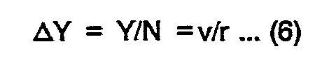
image bar 41 must experience to fully compensate for the cross-line motion of therecording medium 13 is:
- Accordingly, it will be understood that a generally rectangular mapping pattern is provided if the rotation of the
mirror 51 not only involves the aforementioned tangential plane component of rotation, a, but also involves a synchronous sagittal plane component of rotation, β, where for small angles:
- While a dual axis driver, such as a dual axis galvo (not shown), could be employed to synchronously provide appropriate tangential and sagittal components of rotation a and β, respectively, for the
mirror 51, the preferred implementation is to tilt the axis ofrotation 53 of themirror 51 at a predetermined angle 6 (Figure 10) relative to the sagittal plane of theprinter 11, where for small sagittal offset or folding angles:
- In that event, the geometrical requirements for a rectangular mapping pattem are substantially satisfied if the angle, y, through which the
mirror 51 is rotated back and forth about its axis ofrotation 53 is selected so that:
- As will be appreciated, the pixel densities dx and dy along the x and y-axes, respectively, of a rectangular mapping pattern are given by:


- Now, by combining equations (9) and (13) to determine the tilt angle, 8, of the axis of
rotation 53 of themirror 51 that will result in a square mapping pattern, it will be apparent that such a mapping pattern requires that
- Asynchronous printers and the like may experience significant variations in the velocity, v, at which the
recording medium 13 is being advanced, but it will be recognized that the rate, r, at which the pixel patterns are generated may be controlled (by means not shown) if need be to more or less continously compensate for any such variations. - Applying equations (14) and (15) to determine, for example, the rate, r, at which the pixel patterns should be generated and angle, 8, at which the axis of
rotation 53 of themirror 51 should be tilted to obtain a square mapping pattern of alternately interlaced, odd and even numbered pixel patterns, it will be seen that the appropriate selections for that specific case are:

- If desired, there may only be partial compensation for the cross-line motion of the
recording medium 13. As a general rule, however, the additional cost and complexity of compensating for such motion is difficult to justify if substantially complete compensation is not provided, unless some special recording lattice or pattern is desired. - Hexagonal pixel mapping patterns, such as shown in Figure 11, are a particularly interesting example of the adaptability of the present invention. They are of interest because it has been shown that hexagonal sampling patterns require the least number of samples/unit area to unambiguously characterize a random image. See, D P Peterson and D H Middleton, "Sampling and Reconstruction of Wave-Number Limited Functions in N-Dimensional Euclidean Spaces" Information and Control, Vol. 5. p. 279 (1962). As is known, each pixel of a hexagonal pattern is spatially displaced equidistantly from its nearest neighbouring pixels. Such a mapping pattern can be readily realized in accordance with this invention, without having to compensate for the cross-line motion of the
recording medium 13. Indeed, the cross-line motion of therecording medium 13 advantageously is utilized to satisfy the geometric requirements of such a mapping pattern. More particularly, as indicated by the representative set of interlaced pixel patterns, S11, a hexagonal pattern repeats itself once for every two pixel patterns (N = 2) patterns. Thus, from Figure 11 it is clear that if the lateral displacement from one pixel pattern to the next is given by ±AX, a hexagonal mapping pattern is provided if the cross-line displacement, ΔY, of successive pixel patterns is selected so that: -


- There are, of course, alternative applications for certain of the concepts of the present invention. For example, the sagittal compensation for the cross-line motion of the
recording medium 13 might be employed independently to cause overwriting of N successive pixel patterns in registered relationship, such as for writing N colours on apolychromatic recording medium 13 or for recording a N level gray scale image by registereing N successive pixel patterns of progressively increasing or decreasing gray scale value. However, the lateral motion is significant for situations wherein the goal is to provide increased spatial addressing capacity for a discrete image bar being that the addressing capacity or resolution of such an image bar is N times its nominal pixel pitch, X, if the optical footprint of the image bar is laterally shifted for each successive pixel pattern as described hereinabove, As will be understood, the cross-line motion of therecording medium 13 is a relative motion with respect to theimage bar 41 which may be introduced in a number of different ways, including by means of a cross-line optical deflection mechanism (not shown). - In view of the foregoing, it will now be understood that the present invention provides a technique for increasing the spatial addressing capacity of discrete image bars. This increased spatial addressing capacity may be used, for example, to increase the resolution of line printers having such image bars, thereby enhancing the quality of the images that are produced. As will be appreciated, the increased spatial addressing capacity that is provided for discrete image bars in accordance with this invention not only reduces their image distorting spatial quantization errors, but also reduces or eliminates unwanted inter-pixel intensity nulls. Moreover, it will be apparent that there are a wide variety of pixel mapping patterns which may be satisfied through the use of the present invention. Furthermore, it will be understood that there are alternative applications for certain aspects of this invention, including the ability to overwrite successive pixel patterns in registered relationship for colour or gray scale recording in printers or displays.
Claims (10)
Applications Claiming Priority (2)
| Application Number | Priority Date | Filing Date | Title |
|---|---|---|---|
| US73335485A | 1985-05-13 | 1985-05-13 | |
| US733354 | 1985-05-13 |
Publications (3)
| Publication Number | Publication Date |
|---|---|
| EP0202088A2 true EP0202088A2 (en) | 1986-11-20 |
| EP0202088A3 EP0202088A3 (en) | 1987-01-28 |
| EP0202088B1 EP0202088B1 (en) | 1990-11-14 |
Family
ID=24947267
Family Applications (1)
| Application Number | Title | Priority Date | Filing Date |
|---|---|---|---|
| EP19860303569 Expired - Lifetime EP0202088B1 (en) | 1985-05-13 | 1986-05-12 | Discrete optical image bars having enhanced spatial addressing capacity |
Country Status (3)
| Country | Link |
|---|---|
| EP (1) | EP0202088B1 (en) |
| JP (1) | JPS61254927A (en) |
| DE (1) | DE3675576D1 (en) |
Cited By (1)
| Publication number | Priority date | Publication date | Assignee | Title |
|---|---|---|---|---|
| CN111183034A (en) * | 2017-10-10 | 2020-05-19 | 优志旺电机株式会社 | Light irradiation device and image forming apparatus |
Citations (6)
| Publication number | Priority date | Publication date | Assignee | Title |
|---|---|---|---|---|
| US4361394A (en) * | 1980-07-25 | 1982-11-30 | Matsushita Electric Industrial Co., Ltd. | Method and apparatus for scanning light beam |
| EP0093583A1 (en) * | 1982-05-04 | 1983-11-09 | Kabushiki Kaisha Toshiba | Apparatus for scanning a plane with light beams |
| GB2138162A (en) * | 1980-02-06 | 1984-10-17 | Canon Kk | Scanning optical system |
| US4492435A (en) * | 1982-07-02 | 1985-01-08 | Xerox Corporation | Multiple array full width electro mechanical modulator |
| US4493549A (en) * | 1980-04-11 | 1985-01-15 | Coulter Systems Corp. | Optical system for imaging an electrophotographic member |
| US4509058A (en) * | 1983-09-22 | 1985-04-02 | Xerox Corporation | Ink jet printing using horizontal interlacing |
-
1986
- 1986-04-25 JP JP61096612A patent/JPS61254927A/en active Pending
- 1986-05-12 DE DE8686303569T patent/DE3675576D1/en not_active Expired - Fee Related
- 1986-05-12 EP EP19860303569 patent/EP0202088B1/en not_active Expired - Lifetime
Patent Citations (6)
| Publication number | Priority date | Publication date | Assignee | Title |
|---|---|---|---|---|
| GB2138162A (en) * | 1980-02-06 | 1984-10-17 | Canon Kk | Scanning optical system |
| US4493549A (en) * | 1980-04-11 | 1985-01-15 | Coulter Systems Corp. | Optical system for imaging an electrophotographic member |
| US4361394A (en) * | 1980-07-25 | 1982-11-30 | Matsushita Electric Industrial Co., Ltd. | Method and apparatus for scanning light beam |
| EP0093583A1 (en) * | 1982-05-04 | 1983-11-09 | Kabushiki Kaisha Toshiba | Apparatus for scanning a plane with light beams |
| US4492435A (en) * | 1982-07-02 | 1985-01-08 | Xerox Corporation | Multiple array full width electro mechanical modulator |
| US4509058A (en) * | 1983-09-22 | 1985-04-02 | Xerox Corporation | Ink jet printing using horizontal interlacing |
Cited By (2)
| Publication number | Priority date | Publication date | Assignee | Title |
|---|---|---|---|---|
| CN111183034A (en) * | 2017-10-10 | 2020-05-19 | 优志旺电机株式会社 | Light irradiation device and image forming apparatus |
| CN111183034B (en) * | 2017-10-10 | 2022-01-18 | 优志旺电机株式会社 | Light irradiation device and image forming apparatus |
Also Published As
| Publication number | Publication date |
|---|---|
| JPS61254927A (en) | 1986-11-12 |
| EP0202088A3 (en) | 1987-01-28 |
| DE3675576D1 (en) | 1990-12-20 |
| EP0202088B1 (en) | 1990-11-14 |
Similar Documents
| Publication | Publication Date | Title |
|---|---|---|
| EP0550189B1 (en) | Electrooptic TIR light modulator image bar having multiple electrodes per pixel | |
| CN1049780C (en) | Combined modulator schemes for spatial light modulators | |
| EP0620676B1 (en) | Process for digital micromirror printer | |
| EP0079958B1 (en) | High resolution optical-addressing apparatus | |
| EP0636997A2 (en) | Spatial light modulation | |
| US4673953A (en) | Interpixel null suppression for optical image bars | |
| JPH02501292A (en) | Multiplexed array exposure device with equiangular scanning exposure area | |
| EP0079946A4 (en) | Electronic imaging apparatus with light valve arrays. | |
| US4940314A (en) | Variable wavelength discrete optical image bars having passively enhanced spatial addressing capacity | |
| US4751659A (en) | Defect compensation for discrete image bars | |
| US4480899A (en) | Two dimensional electro-optic modulator and applications therefor | |
| US4560994A (en) | Two dimensional electro-optic modulator for printing | |
| US4707743A (en) | Method and apparatus for image conversion with multiple exposures for filtering | |
| EP0412037A2 (en) | Multiple laser beam scanning optics | |
| CA1176742A (en) | Thick film line modulator | |
| EP0202088B1 (en) | Discrete optical image bars having enhanced spatial addressing capacity | |
| US4805012A (en) | System for high resolution exposure address with coarser resolution exposing array | |
| US4438461A (en) | Integrated input/output scanner for electronic document processing | |
| WO1982004368A1 (en) | Improved high-resolution light valve apparatus for electronic imaging | |
| EP0375431B1 (en) | Bandwidth reduced multi-pass writing of variable gray level digital images | |
| JPH0752259B2 (en) | Combination of variable wavelength individual optical image bar and optical system | |
| JP3335394B2 (en) | Optical image bar | |
| EP0747777B1 (en) | Colour printer with a single pass of the photoreceptor | |
| JP3335396B2 (en) | Optical image bar | |
| US5255118A (en) | Electrooptic TIR light modulator image bar having electrode length for optimizing spatial frequency response |
Legal Events
| Date | Code | Title | Description |
|---|---|---|---|
| PUAI | Public reference made under article 153(3) epc to a published international application that has entered the european phase |
Free format text: ORIGINAL CODE: 0009012 |
|
| AK | Designated contracting states |
Kind code of ref document: A2 Designated state(s): DE FR GB |
|
| PUAL | Search report despatched |
Free format text: ORIGINAL CODE: 0009013 |
|
| AK | Designated contracting states |
Kind code of ref document: A3 Designated state(s): DE FR GB |
|
| 17P | Request for examination filed |
Effective date: 19870709 |
|
| 17Q | First examination report despatched |
Effective date: 19881207 |
|
| GRAA | (expected) grant |
Free format text: ORIGINAL CODE: 0009210 |
|
| AK | Designated contracting states |
Kind code of ref document: B1 Designated state(s): DE FR GB |
|
| REF | Corresponds to: |
Ref document number: 3675576 Country of ref document: DE Date of ref document: 19901220 |
|
| ET | Fr: translation filed | ||
| PLBE | No opposition filed within time limit |
Free format text: ORIGINAL CODE: 0009261 |
|
| STAA | Information on the status of an ep patent application or granted ep patent |
Free format text: STATUS: NO OPPOSITION FILED WITHIN TIME LIMIT |
|
| 26N | No opposition filed | ||
| PGFP | Annual fee paid to national office [announced via postgrant information from national office to epo] |
Ref country code: DE Payment date: 19940224 Year of fee payment: 9 |
|
| PGFP | Annual fee paid to national office [announced via postgrant information from national office to epo] |
Ref country code: FR Payment date: 19940310 Year of fee payment: 9 |
|
| PGFP | Annual fee paid to national office [announced via postgrant information from national office to epo] |
Ref country code: GB Payment date: 19940329 Year of fee payment: 9 |
|
| PG25 | Lapsed in a contracting state [announced via postgrant information from national office to epo] |
Ref country code: GB Effective date: 19950512 |
|
| GBPC | Gb: european patent ceased through non-payment of renewal fee |
Effective date: 19950512 |
|
| PG25 | Lapsed in a contracting state [announced via postgrant information from national office to epo] |
Ref country code: DE Effective date: 19960201 |
|
| PG25 | Lapsed in a contracting state [announced via postgrant information from national office to epo] |
Ref country code: FR Effective date: 19960229 |
|
| REG | Reference to a national code |
Ref country code: FR Ref legal event code: ST |
|
| REG | Reference to a national code |
Ref country code: FR Ref legal event code: ST |