EP0202755A1 - Double heterojunction field effect transistor data storage device - Google Patents
Double heterojunction field effect transistor data storage device Download PDFInfo
- Publication number
- EP0202755A1 EP0202755A1 EP86302730A EP86302730A EP0202755A1 EP 0202755 A1 EP0202755 A1 EP 0202755A1 EP 86302730 A EP86302730 A EP 86302730A EP 86302730 A EP86302730 A EP 86302730A EP 0202755 A1 EP0202755 A1 EP 0202755A1
- Authority
- EP
- European Patent Office
- Prior art keywords
- layer
- charge
- gaas
- charge transfer
- substrate
- Prior art date
- Legal status (The legal status is an assumption and is not a legal conclusion. Google has not performed a legal analysis and makes no representation as to the accuracy of the status listed.)
- Withdrawn
Links
- 230000005669 field effect Effects 0.000 title claims abstract description 7
- 238000013500 data storage Methods 0.000 title claims description 4
- 229910001218 Gallium arsenide Inorganic materials 0.000 claims abstract description 21
- 230000004888 barrier function Effects 0.000 claims abstract description 14
- 239000000758 substrate Substances 0.000 claims description 16
- 239000004065 semiconductor Substances 0.000 claims description 15
- 239000000463 material Substances 0.000 claims description 10
- 239000013078 crystal Substances 0.000 claims description 5
- 230000002441 reversible effect Effects 0.000 abstract description 2
- 238000010586 diagram Methods 0.000 description 10
- 230000002596 correlated effect Effects 0.000 description 5
- 230000004044 response Effects 0.000 description 4
- XUIMIQQOPSSXEZ-UHFFFAOYSA-N Silicon Chemical compound [Si] XUIMIQQOPSSXEZ-UHFFFAOYSA-N 0.000 description 3
- 239000002019 doping agent Substances 0.000 description 3
- 238000000034 method Methods 0.000 description 3
- 230000000717 retained effect Effects 0.000 description 3
- 229910052710 silicon Inorganic materials 0.000 description 3
- 239000010703 silicon Substances 0.000 description 3
- 230000004308 accommodation Effects 0.000 description 2
- 229910052751 metal Inorganic materials 0.000 description 2
- 239000002184 metal Substances 0.000 description 2
- 238000001451 molecular beam epitaxy Methods 0.000 description 2
- 239000004411 aluminium Substances 0.000 description 1
- 229910052782 aluminium Inorganic materials 0.000 description 1
- XAGFODPZIPBFFR-UHFFFAOYSA-N aluminium Chemical compound [Al] XAGFODPZIPBFFR-UHFFFAOYSA-N 0.000 description 1
- 238000003486 chemical etching Methods 0.000 description 1
- 238000005530 etching Methods 0.000 description 1
- 239000012212 insulator Substances 0.000 description 1
- 230000007246 mechanism Effects 0.000 description 1
- 238000001020 plasma etching Methods 0.000 description 1
- 238000010561 standard procedure Methods 0.000 description 1
- 238000006467 substitution reaction Methods 0.000 description 1
Images
Classifications
-
- H—ELECTRICITY
- H01—ELECTRIC ELEMENTS
- H01L—SEMICONDUCTOR DEVICES NOT COVERED BY CLASS H10
- H01L29/00—Semiconductor devices adapted for rectifying, amplifying, oscillating or switching, or capacitors or resistors with at least one potential-jump barrier or surface barrier, e.g. PN junction depletion layer or carrier concentration layer; Details of semiconductor bodies or of electrodes thereof ; Multistep manufacturing processes therefor
- H01L29/02—Semiconductor bodies ; Multistep manufacturing processes therefor
- H01L29/12—Semiconductor bodies ; Multistep manufacturing processes therefor characterised by the materials of which they are formed
- H01L29/20—Semiconductor bodies ; Multistep manufacturing processes therefor characterised by the materials of which they are formed including, apart from doping materials or other impurities, only AIIIBV compounds
- H01L29/201—Semiconductor bodies ; Multistep manufacturing processes therefor characterised by the materials of which they are formed including, apart from doping materials or other impurities, only AIIIBV compounds including two or more compounds, e.g. alloys
- H01L29/205—Semiconductor bodies ; Multistep manufacturing processes therefor characterised by the materials of which they are formed including, apart from doping materials or other impurities, only AIIIBV compounds including two or more compounds, e.g. alloys in different semiconductor regions, e.g. heterojunctions
-
- H—ELECTRICITY
- H01—ELECTRIC ELEMENTS
- H01L—SEMICONDUCTOR DEVICES NOT COVERED BY CLASS H10
- H01L29/00—Semiconductor devices adapted for rectifying, amplifying, oscillating or switching, or capacitors or resistors with at least one potential-jump barrier or surface barrier, e.g. PN junction depletion layer or carrier concentration layer; Details of semiconductor bodies or of electrodes thereof ; Multistep manufacturing processes therefor
- H01L29/66—Types of semiconductor device ; Multistep manufacturing processes therefor
- H01L29/68—Types of semiconductor device ; Multistep manufacturing processes therefor controllable by only the electric current supplied, or only the electric potential applied, to an electrode which does not carry the current to be rectified, amplified or switched
- H01L29/76—Unipolar devices, e.g. field effect transistors
- H01L29/772—Field effect transistors
- H01L29/778—Field effect transistors with two-dimensional charge carrier gas channel, e.g. HEMT ; with two-dimensional charge-carrier layer formed at a heterojunction interface
-
- H—ELECTRICITY
- H01—ELECTRIC ELEMENTS
- H01L—SEMICONDUCTOR DEVICES NOT COVERED BY CLASS H10
- H01L29/00—Semiconductor devices adapted for rectifying, amplifying, oscillating or switching, or capacitors or resistors with at least one potential-jump barrier or surface barrier, e.g. PN junction depletion layer or carrier concentration layer; Details of semiconductor bodies or of electrodes thereof ; Multistep manufacturing processes therefor
- H01L29/66—Types of semiconductor device ; Multistep manufacturing processes therefor
- H01L29/68—Types of semiconductor device ; Multistep manufacturing processes therefor controllable by only the electric current supplied, or only the electric potential applied, to an electrode which does not carry the current to be rectified, amplified or switched
- H01L29/76—Unipolar devices, e.g. field effect transistors
- H01L29/772—Field effect transistors
- H01L29/80—Field effect transistors with field effect produced by a PN or other rectifying junction gate, i.e. potential-jump barrier
- H01L29/802—Field effect transistors with field effect produced by a PN or other rectifying junction gate, i.e. potential-jump barrier with heterojunction gate, e.g. transistors with semiconductor layer acting as gate insulating layer, MIS-like transistors
- H01L29/803—Programmable transistors, e.g. with charge-trapping quantum well
Definitions
- the invention relates to a double heterojunction field effect transistor data storage device.
- HEMT high electron mobility transistors
- a number of electrons are trapped in a potential well which appears at a lattice matched heterojunction with a band offset.
- the speed of response substantially increases.
- Such a structure has been known also as a modulation doped and an electron gas type structure.
- US-A-4,163,237 The use of one material of the heterojunction as the gate of a FET with a contiguous region thereto used to move the potential well with respect to the Fermi level for the purpose of setting a specific threshold, is disclosed in EP-A-114762.
- a semiconductor electronically erasable memory structure involving varying insulator properties adjacent to a silicon FET channel is shown in J Applied Phys 50 (9), September 1979, page 5826.
- the invention seeks to provide a double heterojunction field effect transistor data storage device.
- Such a device comprises, according to the invention, a substrate of single crystal semiconductor material having disposed therein spaced apart source and drain regions defining a channel region there-between, a gate layer of single crystal semiconductor material which has a larger bandgap than that of the substrate, forming a heterojunction with the substrate and disposed over the channel region, a charge storage layer of semiconductor material forming a heterojunction with the gate layer and disposed over the channel region, the energy band difference between the gate and charge storage layers being substantially equal to that between the substrate and the gate layer, charge transfer means, having an asymmetric charge transfer characteristic, contiguous with the face of the charge storage layer opposite to that forming the heterojunction with the gate layer and charge introduction and removal means contiguous with the charge transfer means.
- the invention is concerned with a band offset heterojunction FET having a charge storage and removal capability that operates to position and retain, in the absence of signal, the potential well with respect to the Fermi level, so that the FET is either in a conducting or non-conducting state.
- a charge is stored in a semiconductor region that forms a barrier with the gate of a band offset heterojunction FET and employs asymmetry in a second barrier to permit charge introduction and removal in response to a signal.
- the preferred embodiment has a substrate 1 formed of a first semiconductor having a relatively small band gap such as GaAs.
- a heterojunction interface 2 exists between the substrate 1 and a second semiconductor 3 having a wider band gap, such as GaxA11.xAs.
- the heterojunction interface 2 provides a potential well that serves as the channel region of the field effect transistor type device.
- the channel at the interface 2 is terminated at heavily doped source 4 and drain 5 regions, each with a respective ohmic electrode 6 and 7.
- a charge storage region 8 forms a barrier 9 with the region 3.
- the region 8 is of GaAs which, having a smaller band gap than that of the Ga x A1 1- x As, provides a heterojunction barrier at 9.
- a charge transfer accommodation region 10 forms a barrier 11 with region 8.
- the charge transfer accommodation region transfers charge to the region 8 in the presence of a signal of one polarity, transfers charge out of the region 8 in the presence of a signal of the opposite polarity while operating to prevent change of charge state of the region 8 in the no signal condition.
- the region 10 is of GaAll. x As, epitaxial with the GaAs region 8 at a heterojunction barrier 11.
- Portion 12 of the region 10 adjacent the barrier 11 of the larger GaAtAs band gap is graded progressively down to GaAs at the barrier 11.
- An ohmic contact for signal introduction purposes is provided with a doped, smaller band gap region 13, such as GaAs, epitaxial with region 10 at the heterojunction barrier 14 and a metal member 15 at the face 16.
- the structure of Figure 1 can be manufactured using most standard techniques in the art capable of crystal perfection, composition and doping control. A preferred technique because of low temperature operation and the ability to make abrupt change is the technique of molecular beam epitaxy.
- the structure of Figure 1 would be made with the substrate 1, region 8 and region 13 of n-type GaAs and regions 3 and 10 of Ga x A1 1-x As with the mole fraction of A1 varying in the region 12. It will be apparent to one skilled in the art that the substrate 1 can be a buffer layer on a larger supporting member not shown.
- the molecular beam epitaxy technique would provide successive layers on the interface 2 of the substrate.
- the first layer would be the Ga x A1 1-x As region 3 grown on the interface 2 with the mole fraction of A1 as shown in Figure 2 sufficiently high, with x around 0.5, to produce the Ga x A1 1-x As.
- the next layer would be the region 8 of GaAs in which, referring to Figures 2 and 3, there would be no A1 introduced but the n dopant would be introduced.
- region 10 to interface 14 would be grown at a constant value of x.
- the final layer would be GaAs grown on interface 14 with, referring to Figures 2 and 3, no A1 mole fraction and n dopant.
- the metal 15 would be vacuum evaporated.
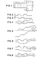
- Figures 4 to 8 illustrates the operation of the device.
- Figure 4 shows the quiescent state of the device.
- Figures 5 and 6 show the way the structure provides the ability to store a charge in response to a signal that will position the potential well across the Fermi level with the condition being retained in the absence of signal.
- Figures 7 and 8 then show the way the charge is removed so that the potential well is no longer across the Fermi level, and that the condition is retained in the absence of signal.
- the energy band diagram of the structure of Figure 1 is shown in the quiescent state wherein the conduction band is in the vicinity of the Fermi level in the regions 13 and 8 and is above the Fermi level in the regions 10 and 3.
- the offset at the potential well at the interface 2 is above the Fermi level so that the device would not conduct.
- a turn-on signal is applied. This condition stores a charge in region 8 which in turn operates to position the potential well across the Fermi level at the interface 2 to establish the conditions for conduction.
- FIG. 7 the relative positions of the band energy diagrams are shown under the conditions where an "off" signal is applied.
- the signal is of a polarity opposite to that of Figure 5 which operates to move the charge out of region 8 toward the inter face 2.
- the graded aspect of portion 12 of region 10 facilitates moving the charge out of region 10.
- the asymmetric barrier in region 10 could also be achieved by a tunnelling - structure.
- the structural configuration provides a charge which moves the conduction band with respect to the Fermi level such that a potential well can be positioned across the Fermi level in one condition at which point conduction can occur or the potential well can be removed from across the Fermi level so that conduction will not occur.
- the substrate 1 is of semi-insulating GaAs and the regions 4 and 5 are doped with silicon to about 10" atoms/cc.
- the ohmic contacts 6 and 7 are standard alloyed AuGe based.
- the region 3 is substantially undoped GaAIAs with the aluminium mole fraction being 0.5 so that it would be described as Ga 0.5 A1 Q0.5 As.
- the region 8 is of GaAs, doped to a concentration of about 10 18 atoms/cc with silicon, as is the region 13.
- the region 9 is of Ga x A1 1-x As with the portion adjacent to the interface 11 provided with a gradually increasing mole fraction of A1 from zero (i.e GaAs) at the interface 11 to Ga o . s A1 0.5 As at the end of portion 12.
- each of the epitaxial regions 3, 8, 12 and 13 is about 50 nm thick.
- the gate structure can be delineated to permit application of the source 4 and drain 5 and contacts 6 and 7 by reactive ion etching or chemical etching. The difference in response to etching by GaAs and GaA1As is usable to expose the interface 2.
- Figure 1 The structure of Figure 1 is responsive to "on” and “off” signals in the 1 to 2 volt range.
- a semiconductor storage device which provides reversible control by conduction in a band offset heterojunction FET by providing an asymmetric barrier controlled charge storage capability that can position a potential well across the Fermi level for conduction, and away from the Fermi level for non-conduction and to retain in that position in the absence of a signal.
Abstract
Description
- The invention relates to a double heterojunction field effect transistor data storage device.
- In devices known as high electron mobility transistors (HEMT), a number of electrons are trapped in a potential well which appears at a lattice matched heterojunction with a band offset. In such a structure when conduction in the channel of a Field Effect Transistor employs such a heterojunction, the speed of response substantially increases. Such a structure has been known also as a modulation doped and an electron gas type structure. Such a structure is disclosed in US-A-4,163,237. The use of one material of the heterojunction as the gate of a FET with a contiguous region thereto used to move the potential well with respect to the Fermi level for the purpose of setting a specific threshold, is disclosed in EP-A-114762. A semiconductor electronically erasable memory structure involving varying insulator properties adjacent to a silicon FET channel is shown in J Applied Phys 50 (9), September 1979, page 5826.
- The invention seeks to provide a double heterojunction field effect transistor data storage device.
- Such a device comprises, according to the invention, a substrate of single crystal semiconductor material having disposed therein spaced apart source and drain regions defining a channel region there-between, a gate layer of single crystal semiconductor material which has a larger bandgap than that of the substrate, forming a heterojunction with the substrate and disposed over the channel region, a charge storage layer of semiconductor material forming a heterojunction with the gate layer and disposed over the channel region, the energy band difference between the gate and charge storage layers being substantially equal to that between the substrate and the gate layer, charge transfer means, having an asymmetric charge transfer characteristic, contiguous with the face of the charge storage layer opposite to that forming the heterojunction with the gate layer and charge introduction and removal means contiguous with the charge transfer means.
- How the invention can be carried out will now be described by way of example, with reference to the accompanying drawings, in which:-
- Figure 1 represents a semiconductor device embodying the invention;
- Figure 2 indicates the mole fraction of A1 in specific regions of a GaAs-Ga 1-xA1xAs embodiment of the invention;
- Figure 3 indicates the n-doping concentration in specific regions of a GaAs-Ga1.,A1xAs embodiment of the invention;
- Figure 4 is a band energy diagram correlated with the structure of Figure 1, indicating the respective energy levels in the quiescent state;
- Figure 5 is a band energy diagram correlated with the structure of Figure 1, indicating the respective energy levels when a charge is being stored that turns the device "on" and produces conduction;
- Figure 6 is a band energy diagram correlated with the structure of Figure 1, indicating the respective energy levels after removal of the charge storage signal that turned the device "on" and produced conduction;
- Figure 7 is a band energy diagram correlated with the structure of Figure 1, indicating the respective energy levels during removal of a charge that produces the "off" or non-conducting condition; and
- Figure 8 is a band energy diagram correlated with Figure 1, after removal of the signal that removed the. charge and produced the non-conducting or "off" condition.
- The invention is concerned with a band offset heterojunction FET having a charge storage and removal capability that operates to position and retain, in the absence of signal, the potential well with respect to the Fermi level, so that the FET is either in a conducting or non-conducting state. A charge is stored in a semiconductor region that forms a barrier with the gate of a band offset heterojunction FET and employs asymmetry in a second barrier to permit charge introduction and removal in response to a signal.
- In the following description of a preferred embodiment of the invention, reference is made to specific semiconductor materials, doping types and concentrations, and physical conduction mechanisms, however, in the light of the principles set forth, various substitutions will be apparent to one skilled in the art.
- Referring to Figure 1, the preferred embodiment has a substrate 1 formed of a first semiconductor having a relatively small band gap such as GaAs. A heterojunction interface 2 exists between the substrate 1 and a
second semiconductor 3 having a wider band gap, such as GaxA11.xAs. The heterojunction interface 2 provides a potential well that serves as the channel region of the field effect transistor type device. The channel at the interface 2 is terminated at heavily doped source 4 and drain 5 regions, each with a respective ohmic electrode 6 and 7. Acharge storage region 8 forms abarrier 9 with theregion 3. Theregion 8 is of GaAs which, having a smaller band gap than that of the GaxA11- xAs, provides a heterojunction barrier at 9. - A charge
transfer accommodation region 10 forms abarrier 11 withregion 8. The charge transfer accommodation region transfers charge to theregion 8 in the presence of a signal of one polarity, transfers charge out of theregion 8 in the presence of a signal of the opposite polarity while operating to prevent change of charge state of theregion 8 in the no signal condition. Theregion 10 is of GaAll. xAs, epitaxial with theGaAs region 8 at aheterojunction barrier 11.Portion 12 of theregion 10 adjacent thebarrier 11 of the larger GaAtAs band gap is graded progressively down to GaAs at thebarrier 11. An ohmic contact for signal introduction purposes is provided with a doped, smallerband gap region 13, such as GaAs, epitaxial withregion 10 at theheterojunction barrier 14 and ametal member 15 at theface 16. - The structure of Figure 1 can be manufactured using most standard techniques in the art capable of crystal perfection, composition and doping control. A preferred technique because of low temperature operation and the ability to make abrupt change is the technique of molecular beam epitaxy. The structure of Figure 1 would be made with the substrate 1,
region 8 andregion 13 of n-type GaAs andregions region 12. It will be apparent to one skilled in the art that the substrate 1 can be a buffer layer on a larger supporting member not shown. - The molecular beam epitaxy technique would provide successive layers on the interface 2 of the substrate. Referring to Figures 2 and 3, the first layer would be the GaxA11-xAs
region 3 grown on the interface 2 with the mole fraction of A1 as shown in Figure 2 sufficiently high, with x around 0.5, to produce the GaxA11-xAs. The next layer would be theregion 8 of GaAs in which, referring to Figures 2 and 3, there would be no A1 introduced but the n dopant would be introduced. The following layer would be theregion 10 in which, again referring to Figures 2 and 3, there would be no n dopant while the mole fraction of A1 would at this point be progressively increased inregion 12 from zero or pure GaAs atinterface 11 to around x = 0.5, thereby grading the band gap of the GaAIAs in theregion 12 adjacent theinterface 11. - The remainder of
region 10 tointerface 14 would be grown at a constant value of x. The final layer would be GaAs grown oninterface 14 with, referring to Figures 2 and 3, no A1 mole fraction and n dopant. Themetal 15 would be vacuum evaporated. - The energy band diagram of Figures 4 to 8 illustrates the operation of the device. Figure 4 shows the quiescent state of the device. Figures 5 and 6 show the way the structure provides the ability to store a charge in response to a signal that will position the potential well across the Fermi level with the condition being retained in the absence of signal. Figures 7 and 8 then show the way the charge is removed so that the potential well is no longer across the Fermi level, and that the condition is retained in the absence of signal.
- Referring to Figure 4, the energy band diagram of the structure of Figure 1 is shown in the quiescent state wherein the conduction band is in the vicinity of the Fermi level in the
regions regions - In Figure 5, a turn-on signal is applied. This condition stores a charge in
region 8 which in turn operates to position the potential well across the Fermi level at the interface 2 to establish the conditions for conduction. - In Figure 6, when the signal is removed, the charge on
region 8 placing the conduction band below the Fermi level cannot leak off due to the gradual shift to a higher band gap in theportion 12 ofregion 10. The charge inregion 8 in turn retains the potential well across the Fermi level in the absence of signal. Thus, once set to "on", the device conducts in the absence of any further signal. - The band energy diagrams in Figures 7 and 8 illustrate the conditions for removal of the charge on
region 8 producing the non-conducting condition. - Referring next to Figure 7, the relative positions of the band energy diagrams are shown under the conditions where an "off" signal is applied. The signal is of a polarity opposite to that of Figure 5 which operates to move the charge out of
region 8 toward the inter face 2. The graded aspect ofportion 12 ofregion 10 facilitates moving the charge out ofregion 10. The asymmetric barrier inregion 10 could also be achieved by a tunnelling - structure. - In Figure 8, after the turn off signal is removed, the band energy diagram is such that the potential well is retained above the Fermi level and consequently no conduction takes place.
- With a signal applied between the substrate 1 and the
gate contact 15, due to the asymmetric storage performance of thelayer 10, charge can be removed via the gate electrode from theregion 8 more easily than it can be added via the channel. This results in the quasi-Fermi level of thelayer 8 being closer to that of thetop layer 13 than to the bottom layer 1. The structural configuration provides a charge which moves the conduction band with respect to the Fermi level such that a potential well can be positioned across the Fermi level in one condition at which point conduction can occur or the potential well can be removed from across the Fermi level so that conduction will not occur. - In a preferred embodiment of the structure of Figure 1, the substrate 1 is of semi-insulating GaAs and the
regions 4 and 5 are doped with silicon to about 10" atoms/cc. The ohmic contacts 6 and 7 are standard alloyed AuGe based. - The
region 3 is substantially undoped GaAIAs with the aluminium mole fraction being 0.5 so that it would be described as Ga0.5A1Q0.5As. Theregion 8 is of GaAs, doped to a concentration of about 1018 atoms/cc with silicon, as is theregion 13. Theregion 9 is of GaxA11-xAs with the portion adjacent to theinterface 11 provided with a gradually increasing mole fraction of A1 from zero (i.e GaAs) at theinterface 11 to Gao.s A10.5As at the end ofportion 12. - In the preferred embodiment, each of the
epitaxial regions - The structure of Figure 1 is responsive to "on" and "off" signals in the 1 to 2 volt range.
- What has been described is a semiconductor storage device which provides reversible control by conduction in a band offset heterojunction FET by providing an asymmetric barrier controlled charge storage capability that can position a potential well across the Fermi level for conduction, and away from the Fermi level for non-conduction and to retain in that position in the absence of a signal.
Claims (6)
Applications Claiming Priority (2)
| Application Number | Priority Date | Filing Date | Title |
|---|---|---|---|
| US72528985A | 1985-04-19 | 1985-04-19 | |
| US725289 | 1985-04-19 |
Publications (1)
| Publication Number | Publication Date |
|---|---|
| EP0202755A1 true EP0202755A1 (en) | 1986-11-26 |
Family
ID=24913932
Family Applications (1)
| Application Number | Title | Priority Date | Filing Date |
|---|---|---|---|
| EP86302730A Withdrawn EP0202755A1 (en) | 1985-04-19 | 1986-04-11 | Double heterojunction field effect transistor data storage device |
Country Status (3)
| Country | Link |
|---|---|
| EP (1) | EP0202755A1 (en) |
| JP (1) | JPS61241968A (en) |
| CA (1) | CA1238719A (en) |
Cited By (8)
| Publication number | Priority date | Publication date | Assignee | Title |
|---|---|---|---|---|
| EP0348099A2 (en) * | 1988-06-21 | 1989-12-27 | AT&T Corp. | Floating gate memories |
| EP0458212A2 (en) * | 1990-05-22 | 1991-11-27 | Nec Corporation | High speed non-volatile programmable read only memory device fabricated by using selective doping technology |
| US5147817A (en) * | 1990-11-16 | 1992-09-15 | Texas Instruments Incorporated | Method for forming programmable resistive element |
| US5206528A (en) * | 1990-11-30 | 1993-04-27 | Nec Corporation | Compound semiconductor field effect transistor having a gate insulator formed of insulative superlattice layer |
| EP0901169A1 (en) * | 1997-09-05 | 1999-03-10 | Hitachi Europe Limited | Controlled conduction device |
| US6060723A (en) * | 1997-07-18 | 2000-05-09 | Hitachi, Ltd. | Controllable conduction device |
| US6169308B1 (en) | 1996-11-15 | 2001-01-02 | Hitachi, Ltd. | Semiconductor memory device and manufacturing method thereof |
| US6642574B2 (en) | 1997-10-07 | 2003-11-04 | Hitachi, Ltd. | Semiconductor memory device and manufacturing method thereof |
Citations (1)
| Publication number | Priority date | Publication date | Assignee | Title |
|---|---|---|---|---|
| EP0114962A2 (en) * | 1982-12-30 | 1984-08-08 | International Business Machines Corporation | Double heterojunction field effect transistors |
-
1986
- 1986-01-17 JP JP61006640A patent/JPS61241968A/en active Pending
- 1986-03-03 CA CA000503081A patent/CA1238719A/en not_active Expired
- 1986-04-11 EP EP86302730A patent/EP0202755A1/en not_active Withdrawn
Patent Citations (1)
| Publication number | Priority date | Publication date | Assignee | Title |
|---|---|---|---|---|
| EP0114962A2 (en) * | 1982-12-30 | 1984-08-08 | International Business Machines Corporation | Double heterojunction field effect transistors |
Non-Patent Citations (4)
| Title |
|---|
| APPLIED PHYSICS LETTERS, vol. 45, no. 12, December 1984, pages 1294-1296, New York, US; S. LURYI et al.: "Hot-electron memory effect in double-layered heterostructures" * |
| IBM TECHNICAL DISCLOSURE BULLETIN, vol. 25, no. 3A, August 1982, page 1250, New York, US; M.H. BRODSKY et al.: "GaAs electrically alterable read-only memory" * |
| JOURNAL OF APPLIED PHYSICS LETTERS, vol. 50, no. 9, September 1979, pages 5826-5829, New York, US; D.J. DiMARIA "Graded or stepped energy band-gap-insulator MIS structures (GI-MIS or SI-MIS)" * |
| PATENT ABSTRACTS OF JAPAN, vol. 8, no. 84 (E-239)[1521], 18th April 1984; & JP-A-59 004 085 (FUJITSU) 10-01-1984 * |
Cited By (13)
| Publication number | Priority date | Publication date | Assignee | Title |
|---|---|---|---|---|
| EP0348099A3 (en) * | 1988-06-21 | 1990-08-22 | American Telephone And Telegraph Company | Floating gate memories |
| EP0348099A2 (en) * | 1988-06-21 | 1989-12-27 | AT&T Corp. | Floating gate memories |
| EP0458212A2 (en) * | 1990-05-22 | 1991-11-27 | Nec Corporation | High speed non-volatile programmable read only memory device fabricated by using selective doping technology |
| EP0458212A3 (en) * | 1990-05-22 | 1992-04-01 | Nec Corporation | High speed non-volatile programmable read only memory device fabricated by using selective doping technology |
| US5147817A (en) * | 1990-11-16 | 1992-09-15 | Texas Instruments Incorporated | Method for forming programmable resistive element |
| US5206528A (en) * | 1990-11-30 | 1993-04-27 | Nec Corporation | Compound semiconductor field effect transistor having a gate insulator formed of insulative superlattice layer |
| US6169308B1 (en) | 1996-11-15 | 2001-01-02 | Hitachi, Ltd. | Semiconductor memory device and manufacturing method thereof |
| US6825527B2 (en) | 1996-11-15 | 2004-11-30 | Hitachi, Ltd. | Semiconductor memory device and manufacturing method |
| US6211531B1 (en) | 1997-07-18 | 2001-04-03 | Hitachi, Ltd. | Controllable conduction device |
| US6060723A (en) * | 1997-07-18 | 2000-05-09 | Hitachi, Ltd. | Controllable conduction device |
| US7132713B2 (en) | 1997-07-18 | 2006-11-07 | Hitachi, Ltd. | Controllable conduction device with electrostatic barrier |
| EP0901169A1 (en) * | 1997-09-05 | 1999-03-10 | Hitachi Europe Limited | Controlled conduction device |
| US6642574B2 (en) | 1997-10-07 | 2003-11-04 | Hitachi, Ltd. | Semiconductor memory device and manufacturing method thereof |
Also Published As
| Publication number | Publication date |
|---|---|
| CA1238719A (en) | 1988-06-28 |
| JPS61241968A (en) | 1986-10-28 |
Similar Documents
| Publication | Publication Date | Title |
|---|---|---|
| US4194935A (en) | Method of making high mobility multilayered heterojunction devices employing modulated doping | |
| US4163237A (en) | High mobility multilayered heterojunction devices employing modulated doping | |
| US5923046A (en) | Quantum dot memory cell | |
| US5640022A (en) | Quantum effect device | |
| US5777364A (en) | Graded channel field effect transistor | |
| US4404732A (en) | Self-aligned extended epitaxy mesfet fabrication process | |
| EP0114962A2 (en) | Double heterojunction field effect transistors | |
| US4740822A (en) | Field effect device maintaining a high speed operation in a high voltage operation | |
| US4772925A (en) | High speed switching field effect transistor | |
| US4878095A (en) | Semiconductor device in particular a hot electron transistor | |
| EP0008898B1 (en) | Method of forming an oxide layer on a group iii-v compound | |
| EP0100529B1 (en) | High speed field-effect transistor employing heterojunction | |
| US6242293B1 (en) | Process for fabricating double recess pseudomorphic high electron mobility transistor structures | |
| US6004137A (en) | Method of making graded channel effect transistor | |
| EP0202755A1 (en) | Double heterojunction field effect transistor data storage device | |
| US6057566A (en) | Semiconductor device | |
| US4600932A (en) | Enhanced mobility buried channel transistor structure | |
| EP0205164B1 (en) | Semiconductor device structure | |
| US5381027A (en) | Semiconductor device having a heterojunction and a two dimensional gas as an active layer | |
| JPH0261151B2 (en) | ||
| EP0602671B1 (en) | Heterojunction field effect transistor having an improved transistor characteristic | |
| US5258631A (en) | Semiconductor device having a two-dimensional electron gas as an active layer | |
| US5311045A (en) | Field effect devices with ultra-short gates | |
| US5107314A (en) | Gallium antimonide field-effect transistor | |
| KR940010557B1 (en) | Semiconductor device |
Legal Events
| Date | Code | Title | Description |
|---|---|---|---|
| PUAI | Public reference made under article 153(3) epc to a published international application that has entered the european phase |
Free format text: ORIGINAL CODE: 0009012 |
|
| AK | Designated contracting states |
Kind code of ref document: A1 Designated state(s): DE FR GB IT |
|
| 17P | Request for examination filed |
Effective date: 19870224 |
|
| 17Q | First examination report despatched |
Effective date: 19890220 |
|
| 18W | Application withdrawn |
Withdrawal date: 19890302 |
|
| STAA | Information on the status of an ep patent application or granted ep patent |
Free format text: STATUS: THE APPLICATION HAS BEEN WITHDRAWN |
|
| R18W | Application withdrawn (corrected) |
Effective date: 19890302 |
|
| RIN1 | Information on inventor provided before grant (corrected) |
Inventor name: KIRCHNER, PETER DANIEL Inventor name: JACKSON, THOMAS NELSON Inventor name: FREEOUF, JOHN LAWRENCE |