EP0206496A2 - Phased array semiconductor laser - Google Patents
Phased array semiconductor laser Download PDFInfo
- Publication number
- EP0206496A2 EP0206496A2 EP86303650A EP86303650A EP0206496A2 EP 0206496 A2 EP0206496 A2 EP 0206496A2 EP 86303650 A EP86303650 A EP 86303650A EP 86303650 A EP86303650 A EP 86303650A EP 0206496 A2 EP0206496 A2 EP 0206496A2
- Authority
- EP
- European Patent Office
- Prior art keywords
- regions
- phased array
- laser
- semiconductor laser
- active region
- Prior art date
- Legal status (The legal status is an assumption and is not a legal conclusion. Google has not performed a legal analysis and makes no representation as to the accuracy of the status listed.)
- Granted
Links
Images

Classifications
-
- H—ELECTRICITY
- H01—ELECTRIC ELEMENTS
- H01S—DEVICES USING THE PROCESS OF LIGHT AMPLIFICATION BY STIMULATED EMISSION OF RADIATION [LASER] TO AMPLIFY OR GENERATE LIGHT; DEVICES USING STIMULATED EMISSION OF ELECTROMAGNETIC RADIATION IN WAVE RANGES OTHER THAN OPTICAL
- H01S5/00—Semiconductor lasers
- H01S5/40—Arrangement of two or more semiconductor lasers, not provided for in groups H01S5/02 - H01S5/30
- H01S5/4025—Array arrangements, e.g. constituted by discrete laser diodes or laser bar
- H01S5/4031—Edge-emitting structures
-
- B—PERFORMING OPERATIONS; TRANSPORTING
- B82—NANOTECHNOLOGY
- B82Y—SPECIFIC USES OR APPLICATIONS OF NANOSTRUCTURES; MEASUREMENT OR ANALYSIS OF NANOSTRUCTURES; MANUFACTURE OR TREATMENT OF NANOSTRUCTURES
- B82Y20/00—Nanooptics, e.g. quantum optics or photonic crystals
-
- H—ELECTRICITY
- H01—ELECTRIC ELEMENTS
- H01S—DEVICES USING THE PROCESS OF LIGHT AMPLIFICATION BY STIMULATED EMISSION OF RADIATION [LASER] TO AMPLIFY OR GENERATE LIGHT; DEVICES USING STIMULATED EMISSION OF ELECTROMAGNETIC RADIATION IN WAVE RANGES OTHER THAN OPTICAL
- H01S5/00—Semiconductor lasers
- H01S5/20—Structure or shape of the semiconductor body to guide the optical wave ; Confining structures perpendicular to the optical axis, e.g. index or gain guiding, stripe geometry, broad area lasers, gain tailoring, transverse or lateral reflectors, special cladding structures, MQW barrier reflection layers
- H01S5/2004—Confining in the direction perpendicular to the layer structure
- H01S5/2009—Confining in the direction perpendicular to the layer structure by using electron barrier layers
- H01S5/2013—MQW barrier reflection layers
-
- H—ELECTRICITY
- H01—ELECTRIC ELEMENTS
- H01S—DEVICES USING THE PROCESS OF LIGHT AMPLIFICATION BY STIMULATED EMISSION OF RADIATION [LASER] TO AMPLIFY OR GENERATE LIGHT; DEVICES USING STIMULATED EMISSION OF ELECTROMAGNETIC RADIATION IN WAVE RANGES OTHER THAN OPTICAL
- H01S5/00—Semiconductor lasers
- H01S5/20—Structure or shape of the semiconductor body to guide the optical wave ; Confining structures perpendicular to the optical axis, e.g. index or gain guiding, stripe geometry, broad area lasers, gain tailoring, transverse or lateral reflectors, special cladding structures, MQW barrier reflection layers
- H01S5/2054—Methods of obtaining the confinement
- H01S5/2059—Methods of obtaining the confinement by means of particular conductivity zones, e.g. obtained by particle bombardment or diffusion
-
- H—ELECTRICITY
- H01—ELECTRIC ELEMENTS
- H01S—DEVICES USING THE PROCESS OF LIGHT AMPLIFICATION BY STIMULATED EMISSION OF RADIATION [LASER] TO AMPLIFY OR GENERATE LIGHT; DEVICES USING STIMULATED EMISSION OF ELECTROMAGNETIC RADIATION IN WAVE RANGES OTHER THAN OPTICAL
- H01S5/00—Semiconductor lasers
- H01S5/30—Structure or shape of the active region; Materials used for the active region
- H01S5/34—Structure or shape of the active region; Materials used for the active region comprising quantum well or superlattice structures, e.g. single quantum well [SQW] lasers, multiple quantum well [MQW] lasers or graded index separate confinement heterostructure [GRINSCH] lasers
- H01S5/343—Structure or shape of the active region; Materials used for the active region comprising quantum well or superlattice structures, e.g. single quantum well [SQW] lasers, multiple quantum well [MQW] lasers or graded index separate confinement heterostructure [GRINSCH] lasers in AIIIBV compounds, e.g. AlGaAs-laser, InP-based laser
- H01S5/34313—Structure or shape of the active region; Materials used for the active region comprising quantum well or superlattice structures, e.g. single quantum well [SQW] lasers, multiple quantum well [MQW] lasers or graded index separate confinement heterostructure [GRINSCH] lasers in AIIIBV compounds, e.g. AlGaAs-laser, InP-based laser with a well layer having only As as V-compound, e.g. AlGaAs, InGaAs
- H01S5/3432—Structure or shape of the active region; Materials used for the active region comprising quantum well or superlattice structures, e.g. single quantum well [SQW] lasers, multiple quantum well [MQW] lasers or graded index separate confinement heterostructure [GRINSCH] lasers in AIIIBV compounds, e.g. AlGaAs-laser, InP-based laser with a well layer having only As as V-compound, e.g. AlGaAs, InGaAs the whole junction comprising only (AI)GaAs
Definitions
- This invention relates to phased array semiconductor lasers having multi-emission or broad emission capabilities and in particular to a phased array laser or phased locked array laser having preferred fundamental supermode operation with a structural design that utilizes impurity-induced disordering-(IID).
- Phased array semiconductor lasers comprise a plurality of clasely-coupled or spaced emitters on the same integral structure or substrate. Examples of such phased array lasers are illustrated in US-A-4 255 717, now Reissue Patent 31 806, and in an article of William Streifer et al, entitled “Phased Array Diode Lasers", published in the June 1984 Issue of Laser FocusIElectro-Optics.
- the emitters of such a laser are represented by the periodically spaced current confinement means, e.g. stripes, for current pumping and establishment of spaced optical cavities in the active region of the structure.
- the current confinement means may be interconnected or closely spaced to a degree that the optical mode established in each of the lasing cavities below a respective current confinement means couples to its neighbouring optical modes, i.e. the evanescent wave overlaps into adjacent optical lasing cavities.
- the optical fields produced become locked in phase, and, if the phase difference between adjacent current confinement means is zero, the lateral radiation pattern in the far field will comprise a single lobe.
- the phased array laser does not operate in a single mode but rather generally operates with two or more lobes in the far field pattern.
- the phase relationship between adjacent optical modes is not under independent control and the phases will adjust themselves in a manner toward minimizing laser threshold current.
- the lasing mode favoured is a supermode wherein the optical field between adjacent optical emitters passes through zero. This is because in most real refractive index lasers, as well as many gain-guided lasers, pumping is reduced at locations between the laser emitters requiring overall reduced current pumping.
- An array laser with N coupled emitters has N possible coupled modes, which are referred to as "supermodes".
- a supermode is a cooperative lasing of the N optical emitters or filaments of the array laser. Since there are N emitters, there are N possible supermodes since all these emitters are optically coupled together.
- Each supermode has the property that the first and the N th supermode have the same intensity pattern or envelope, the second and the (N-1 ) th have the same intensity envelope, and, in general, the i th and (N-i) th have the same intensity envelopes.
- the first or fundamental supermode has all emitters lasing in phase with an amplitude distribution representive of half a sinusoidal cycle. This is the only supermode pattern that radiates in a single central lobe in the far field pattern because all emitters are in phase.
- the first and N th supermode envelopes are half a sinusoidal period
- the second and the (N-1) th supermode envelopes are two half sinusoidal periods, etc.
- the phase relationship between the individual emitters in N supermodes differ. Specifically, for the first supermode, all emitters are in phase, and for the N th supermode, the phases alternate between zero and ⁇ .
- the first and N th supermodes have the lowest current thresholds compared with all other supermodes because their intensity envelopes do not exhibit nulls near the centre of the array where the charge density is greater as a result of current spreading and charge diffusion in the active region of the array laser.
- the N th supermode which radiates in two lobes, has a lower current threshold of operation than the first supermode.
- Phased array lasers have high utility because of their high power output. It is preferred that the power be concentrated in a single lobe, i.e., in the first supermode. The reason is that a substantial majority of laser applications require power in a single far field lobe. If lasing is experienced in more than one lobe, measures are taken to diminish or otherwise attempt to eliminate or block off the other operating lobes in the far field pattern.
- the present invention represents an improved phased array semiconductor laser providing the desired fundamental supermode operation but utilizing a more streamline structural configuration providing a much simpler method of fabrication by employing impurity induced disordering (IID) techniques.
- IID impurity induced disordering
- phased array semiconductor lasers provide fundamental or preferred first supermode operation wherein fabrication is accomplished by a single, continuous fabricating process followed by impurity-induced disordering - (IID), e.g. the impurity diffusion technique or the implant/anneal technique as known in the art.
- IID impurity-induced disordering -
- Fundamental supermode selection is accomplished by providing a multiquantum well superiattice as a cladding layer in the phased array laser structure in combination with the conventional single semiconductor cladding layer, which is followed by spatially disposed impurity-induced disordering regions extending through the superlattice to form regions capable of providing higher gain compared with adjacent regions not experiencing impurity-induced disordering.
- the adjacent regions without impurity-induced disordering contain unspoiled superlattice regions that provide higher real index waveguiding compared with the adjacent disordered regions, with the diffusions in the disordered regions have higher conductivity properties compared with the remaining ordered regions and are, therefore, more efficiently pumped electrically.
- disordered regions form alternating higher gain regions offset between regions of nondisordered waveguide regions having higher real index waveguiding properties but lower gain properties, thereby fulfiling the conditions necessary to provide fundamental or preferred first supermode operation.
- the active region of the phased array semiconductor laser of this invention may comprise a con- venfional active layer on an active region comprising a single quantum well or multiple quantum well.
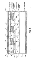
- the semiconductor layers comprising the phase array semiconductors lasers 10 and 30 of Figures 1 and 2 are not shown to scale, in order to illustrate the features of this invention.
- Phase-locked array laser 10 is illustrated in the III-V material regime of GaAs/GaAIAs.
- Laser 10 comprises a substrate 12 of n-GaAs upon which is epitaxially deposited a cladding layer 14 of n-Ga 1-x ALxAs; an active region 16 being undoped, or p-type or n-type and can comprise any active region structure commonly known in the art including, for example, a GaAs layer, for example, 50 nm to 500 nm thick, or a single quantum well of either GaAs or Ga i .
- yAlyAs where y is very small and x > y or a multiple quantum well structure of alternating well layers of GaAs or Ga 1-y Al y As and corresponding barrier layers of either AlAs or Ga 1-y Al y As, or a separate single or multiple quantum well structure in a separate confinement cavity; a cladding layer 18 of p-Ga 1-z Al As where x, z > y; a multilayer n-type or p-type superlattice 20 comprising altsmat- ing well layers of GaAs or Ga 1-w Al w As with barrier layers of either AlAs or Ga 1-w Al w As or AlAs wherein x, z, w, > y', w' > y; and cap layer 22 of p + GaAs.
- cladding layer 14 may be in the range of 0.5 to 1.0 ⁇ m and active region 16 may be a conventional double heterostructure having an active layer thickness of 50 nm to 500 nm thick or a quantum well structure wherein the quantum wells of GaAs may be about 3 nm -50 nm thick and the barrier layers of Ga 1-y AL y As may be about 1 nm -10 nm thick with y in the range of 0.1 to 0.4.
- Cladding layer 18 may be in the range of 0.1 to 1.0 ⁇ m.
- Superlattice 20 may be in the range of 0.01 to 1.0 ⁇ m wherein the quantum wells of GaAs may be about 4 nm thick and the barrier layers of Ga 1-Y Al y As may be about 6 nm thick.
- Cap layer 22 may be in the range of 0.1 to 1.0 um.
- IID impurity-induced disordering
- Diffusion disordering is exemplified in US-A-4 378 255 wherein there is taught the technique of selectively disordering a multiple quantum well structure or supsriattice in a semiconductor device through the employment of a zinc diffusion, causing' an upward shifting of the bandgap of the disordered material compared with regions of the multiple quantum well structure where disordering has not occurred.
- Such diffusions can be generally carried out in a temperature range of 500°C -600°C, which is lower than the epigrowth temperature of III-V materials, which is about 750"C.
- Such disordering is also possible with other elements such as Si, Ge and Sn but at higher temperatures, e.g., about 675°C.
- disordering is possible through implantation of elements acting as shallow or deep level impurities, such as, Se, Mg, Sn, O, S, Be, Te, Si, Mn, Zn, Cd, Ln, Cr or Kr followed by a high temperature anneal best performed in an As environment in the case of III-V epigrowth to prevent the outdiffusion of As from the growth.
- impurity implant followed by an anneal the anneal temperatures are relatively at higher temperatures compared with diffusion temperatures, e.g. above 800°C.
- these types of disordering are not limited to species traditionally considered as impurities but also can be extended to include any species that either disorders the crystal through diffusion or damages the crystal, the annealing of the damaged crystal creating the disordered crystal.
- a Si3N. mask is formed on the top surface of layer 22 with openings exposing regions of the laser structure to impurity diffusion.
- the masks protect regions forming a series of laser optical cavities or elements having facet emission points 17 and that are sufficiently close to one another so as to provide optically coupled adjacent emitters, i.e. the evanescent wave of neighbouring optical cavity overlaps into adjacent optical cavities.
- the current confinement means and desired refractive index profile are established by selectively diffusing a high concentration p impurity into the exposed regions of the laser structure.
- a high concentration p impurity For example, zinc may be selectively diffused at 700°C for a sufficient period in a semi-sealed graphite boat containing appropriate diffusion sources. This type of process would by typically carried out in a hydrogen flow.
- the diffusion of the superlattice 20 causes an intermixing of AI and Ga in the GaAs-GaAlAs superlattice, resulting in a GaAIAs alloy of averaged AlAs mole fraction illustrated as IID regions 28 in Figure 1.
- the diffusion of zinc is accomplished at a relatively low temperature, such as, 700°C and is maintained only so long as to reach the depth of or penetrate cladding layer 18, as indicated at points 29. It is preferred not to extend the zinc diffusion across the laser active region because this extension of the diffusion region creates problems with parasitic p-n junctions in the laser structure and with free carrier absorption in the laser optical cavities.
- conventional metal contacts 24 and 26 are applied respectively to the surface of cap layer 22 and bottom surface of substrate 12.
- the array of zinc diffused regions 28 serve the dual function of smearing out or disordering the superlattice 20 to provide an index profile for guiding the propogation of radiation along the optical cavity of each laser element, represented by dotted line 27A, and also provides slightly more preferred current paths to regions 28 through the p-type disordered superlattice for current injection into ac- five region 16 in the general regions depicted by dotted line 27A. Because of the lower index profile provided by IID regions 28, the structure encourages operation of the array of lasers with a single lobe far field pattern. Also, because of the n-type layers chosen for superlattice 20, current injection is more confined to zinc diffused p-type layers of regions 28.
- the resulting laser structure in the plane of superlattice 20 is such that a plurality of higher index guiding regions 27 are provided in the nondisordered areas of superlattice 20. These regions provided for enhanced waveguiding because of a higher refractive index compared with regions 28.
- regions 28 provide areas of higher conductivity or less resistance to current flow, vis-a-vis nondisordered regions 27, so that with the application of a voltage cross metal contacts 24 and 26, current flow will be substantially confined to and through IID regions 28. Current will also flow through region 27A because of the lateral diffusion of carriers.
- the structure of laser 10 achieves the results of those structures with a simpler and easier to fabricate array laser structure, which provides a higher single mode output power capability as well as improved optical field mode control through the use of IID techniques.
- some array laser structures of the prior art require a proton bombardment definition for current confinement means, which is not necessary relative to the laser structures of this invention.
- a virtually symmetric waveguiding structure may be maintained at regions depicted by dotted line 27A by designing individual compositional components of the p side cladding region comprising cladding layer 18 and superlattice 20 to have a combined refractive index at regions 27 and 27A to have a substantially identical refractive index as n side cladding layer 14.
- a supertattice may likewise be formed in the bottom or n side cladding layer 14 either alone or in combination with p side clad supertattice 20. As a uperlattice cladding combination, a full length optical cavity index guide would be established.
- array laser 30 is of identical structure to array laser 10, except that the impurity types of the respective semiconductor layers comprising the laser structure are reversed.
- Laser 30 comprises a substrate 32 of P-Ga-As upon which is epitaxially deposited a cladding layer 34 of p-Ga i . x AL x As; an active region structure commonly known in the art as previously exemplified in Figure 1 relative to region 16; a cladding layer 38 of n-Ga 1-z AL z As where x, z > y, multilayer n or p type superlattice 40 comprising alternating well layers of materials previously exemplified in Figure 1 relative to supertattice 20; and a cap layer of n + GaAs.
- layer thicknesses for the structural layes of laser 30 may be in the ranges exemplified for the corresponding layers of laser 10.
- a Si 3 N 4 mask is formed on the top regions of layer 42 with openings exposing regions of the. laser structure to IID techniques as previously explained.
- a series of laser elements with emission points 47 are formed that at sufficiently close to another another so as to provide optically coupled adjacent emitters, i.e. the evanescent wave of a neighbouring optical cavity overlaps into adjacent cavities.
- the establishment of the current confinement means and refractive index profile are established in the manner previously explained, except an n-type diffusant, e.g. silicon, tin or germanium, is utilized to disorder the superlattice structures in regions 38 to a depth into cladding layer 38 not to penetrate the active region 36 forming optical guide regions 47A.
- conventional metal contacts 44 and 46 are applied respectively to the surface of cap layer 42 and bottom surface of substrate 32.
- the array of silicon diffused regons 48 serve the dual function of smearing out or disordering the superlattice 40 to provide an index profile for guiding the propogation of radiation along the optical cavity of each laser element, represented by dotted line 47A, and also provides slightly more preferred current paths at regions 48 through the n-type disordered superlattice for current injection into active region 36 in the general regions depicted by dotted line 47A. Because of the lower index profile provided by IID regions 48, the structure encourages operation of the array of lasers with a single lobe far field pattern. Also, because of the p-type layers chosen for superlattice 40, current injection is more confined to silicon diffused n-type layers of regions 48.
- the resulting laser structure in the plane of superlattice 40 is such that a plurality of higher index guiding regions 47 are provided in the nondisordered areas of superlattice 40. These regions provide for enhanced waveguiding because of a higher refractive index compared with regions 48.
- regions 48 provide areas of higher conductivity or less resistance to current flow, vis-a-vis nondisordered regions 47, so that with the application of a voltage across metal contacts 44 and 46, current flow will be substantially confined to and through IID regions 48. Current will also flow through region 47A because of the lateral diffusion of carriers.
- a superlattice may likewise be formed in the bottom or p side cladding layer 34 either alone or in combination with n side clad superlattice 40. As a supertattice cladding combination, a full length optical cavity index guide would be established.
- the p + type diffused regions 28 may be n + type diffused regions, e.g. silicon, so long as the background doping of superlattice 20 is p type.
- the n + type diffused regions 48 may be p + type diffused regions, e.g. zinc, so long as the background doping of superiattice 40 is n type.
- the active region may comprise a single active layer or, alternatively, may comprise an active region of either single quantum well or multiquantum well.
Abstract
Description
- This invention relates to phased array semiconductor lasers having multi-emission or broad emission capabilities and in particular to a phased array laser or phased locked array laser having preferred fundamental supermode operation with a structural design that utilizes impurity-induced disordering-(IID).
- Phased array semiconductor lasers comprise a plurality of clasely-coupled or spaced emitters on the same integral structure or substrate. Examples of such phased array lasers are illustrated in US-A-4 255 717, now Reissue Patent 31 806, and in an article of William Streifer et al, entitled "Phased Array Diode Lasers", published in the June 1984 Issue of Laser FocusIElectro-Optics. The emitters of such a laser are represented by the periodically spaced current confinement means, e.g. stripes, for current pumping and establishment of spaced optical cavities in the active region of the structure. The current confinement means may be interconnected or closely spaced to a degree that the optical mode established in each of the lasing cavities below a respective current confinement means couples to its neighbouring optical modes, i.e. the evanescent wave overlaps into adjacent optical lasing cavities. The optical fields produced become locked in phase, and, if the phase difference between adjacent current confinement means is zero, the lateral radiation pattern in the far field will comprise a single lobe. However, as explained in the above-mentioned article, the phased array laser does not operate in a single mode but rather generally operates with two or more lobes in the far field pattern. The phase relationship between adjacent optical modes is not under independent control and the phases will adjust themselves in a manner toward minimizing laser threshold current. In most cases, it appears that the lasing mode favoured is a supermode wherein the optical field between adjacent optical emitters passes through zero. This is because in most real refractive index lasers, as well as many gain-guided lasers, pumping is reduced at locations between the laser emitters requiring overall reduced current pumping.
- The foregoing explanation can be exemplified as follows. An array laser with N coupled emitters has N possible coupled modes, which are referred to as "supermodes". A supermode is a cooperative lasing of the N optical emitters or filaments of the array laser. Since there are N emitters, there are N possible supermodes since all these emitters are optically coupled together.
- Each supermode has the property that the first and the Nthsupermode have the same intensity pattern or envelope, the second and the (N-1 )th have the same intensity envelope, and, in general, the ith and (N-i)th have the same intensity envelopes. The first or fundamental supermode has all emitters lasing in phase with an amplitude distribution representive of half a sinusoidal cycle. This is the only supermode pattern that radiates in a single central lobe in the far field pattern because all emitters are in phase.
- Thus, for a uniformly spaced array of identical emitters, the first and Nth supermode envelopes are half a sinusoidal period, the second and the (N-1) th supermode envelopes are two half sinusoidal periods, etc. The phase relationship between the individual emitters in N supermodes differ. Specifically, for the first supermode, all emitters are in phase, and for the Nth supermode, the phases alternate between zero and π. Usually the first and Nth supermodes have the lowest current thresholds compared with all other supermodes because their intensity envelopes do not exhibit nulls near the centre of the array where the charge density is greater as a result of current spreading and charge diffusion in the active region of the array laser.
- However, as previously indicated, the Nth supermode, which radiates in two lobes, has a lower current threshold of operation than the first supermode.
- Phased array lasers have high utility because of their high power output. It is preferred that the power be concentrated in a single lobe, i.e., in the first supermode. The reason is that a substantial majority of laser applications require power in a single far field lobe. If lasing is experienced in more than one lobe, measures are taken to diminish or otherwise attempt to eliminate or block off the other operating lobes in the far field pattern.
- Recently, there has been much activity relative to phase-locked array lasers or phased-array lasers where efforts have been established to discriminate among the supermodes and provide fundamental supermode selection. One such suggestion was made at the IEEE 9th Conference in Brazil, July, 1984 wherein J Katz et al presented a talk on supermode discrimination by controlling lateral gain distribution along the plane of the lasing elements by incorporating a separate contact in each laser array element and tailoring the currents through the array laser elements. The abstract for the talk is found in the Proceedings of the Conference at pages 94 and 95 entitled "Supermode Discrimination in Phase-Locked Arrays of Semiconductor Laser Arrays".
- More recent are the articles of Twu et al entitled "High Power Coupled Ridge Waveguide Semiconductor Laser Arrays", Applied Physics Letters, Vol. 45(7), pp. 709-711 (October 1, 1984) and of S Mukai et al entitled Fundamental Mode Oscillation of Buried Ridge Waveguide Laser Array", Applied Physics Letters, Vol. 45(8), pp. 834-835 - (October 15, 1984). These articles suggest discrimination among the supermodes to obtain the single lobe fundamental supermode by employing index-guided ridge waveguide structure, wherein the laser elements are uniformly pumped with the optical field mainly confined to the ridge region of the structure white higher gain is experienced in the valley or coupling regions to induce in-phase operation (0° phase) and promotion of fundamental supermode operation.
- The present invention represents an improved phased array semiconductor laser providing the desired fundamental supermode operation but utilizing a more streamline structural configuration providing a much simpler method of fabrication by employing impurity induced disordering (IID) techniques.
- According to this invention, phased array semiconductor lasers provide fundamental or preferred first supermode operation wherein fabrication is accomplished by a single, continuous fabricating process followed by impurity-induced disordering - (IID), e.g. the impurity diffusion technique or the implant/anneal technique as known in the art. Fundamental supermode selection is accomplished by providing a multiquantum well superiattice as a cladding layer in the phased array laser structure in combination with the conventional single semiconductor cladding layer, which is followed by spatially disposed impurity-induced disordering regions extending through the superlattice to form regions capable of providing higher gain compared with adjacent regions not experiencing impurity-induced disordering. The adjacent regions without impurity-induced disordering contain unspoiled superlattice regions that provide higher real index waveguiding compared with the adjacent disordered regions, with the diffusions in the disordered regions have higher conductivity properties compared with the remaining ordered regions and are, therefore, more efficiently pumped electrically. As a result, disordered regions form alternating higher gain regions offset between regions of nondisordered waveguide regions having higher real index waveguiding properties but lower gain properties, thereby fulfiling the conditions necessary to provide fundamental or preferred first supermode operation.
- The active region of the phased array semiconductor laser of this invention may comprise a con- venfional active layer on an active region comprising a single quantum well or multiple quantum well.
- The present invention will now be described by way of example with reference to the accompanying drawings, in which:
- Figure 1 schematically illustrates a side elevation of a first embodiment of the phased array semiconductor laser of this invention, and
- Figure 2 schematically illustrates a side elevation of a second embodiment of the phased array semiconductor laser of this invention.
- The semiconductor layers comprising the phase
array semiconductors lasers - Referece is now made to Figure 1 wherein there is illustrated a first embodiment of the phased array semiconductor laser of this invention. Phase-locked
array laser 10 is illustrated in the III-V material regime of GaAs/GaAIAs.Laser 10 comprises asubstrate 12 of n-GaAs upon which is epitaxially deposited acladding layer 14 of n-Ga1-x ALxAs; anactive region 16 being undoped, or p-type or n-type and can comprise any active region structure commonly known in the art including, for example, a GaAs layer, for example, 50 nm to 500 nm thick, or a single quantum well of either GaAs or Gai. yAlyAs where y is very small and x > y or a multiple quantum well structure of alternating well layers of GaAs or Ga1-yAlyAs and corresponding barrier layers of either AlAs or Ga1-yAly As, or a separate single or multiple quantum well structure in a separate confinement cavity; acladding layer 18 of p-Ga1-zAl As where x, z > y; a multilayer n-type or p-type superlattice 20 comprising altsmat- ing well layers of GaAs or Ga1-wAlwAs with barrier layers of either AlAs or Ga1-w AlwAs or AlAs wherein x, z, w, > y', w' > y; andcap layer 22 of p+ GaAs. There may be a thin n-GaAs buffer layer deposited onsubstrate 12 prior to deposition of layers 14-22. - As an example of typical layer thicknesses,
cladding layer 14 may be in the range of 0.5 to 1.0 µm andactive region 16 may be a conventional double heterostructure having an active layer thickness of 50 nm to 500 nm thick or a quantum well structure wherein the quantum wells of GaAs may be about 3 nm -50 nm thick and the barrier layers of Ga1-yALyAs may be about 1 nm -10 nm thick with y in the range of 0.1 to 0.4. Claddinglayer 18 may be in the range of 0.1 to 1.0 µm. Superlattice 20 may be in the range of 0.01 to 1.0 µm wherein the quantum wells of GaAs may be about 4 nm thick and the barrier layers of Ga1-YAlyAs may be about 6 nm thick.Cap layer 22 may be in the range of 0.1 to 1.0 um. - To form a multicavity array laser, impurity-induced disordering (IID) techniques known in the art may be utilized, e.g. diffusion disordering or implant/anneal disordering. Diffusion disordering is exemplified in US-A-4 378 255 wherein there is taught the technique of selectively disordering a multiple quantum well structure or supsriattice in a semiconductor device through the employment of a zinc diffusion, causing' an upward shifting of the bandgap of the disordered material compared with regions of the multiple quantum well structure where disordering has not occurred. Such diffusions can be generally carried out in a temperature range of 500°C -600°C, which is lower than the epigrowth temperature of III-V materials, which is about 750"C.
- Such disordering is also possible with other elements such as Si, Ge and Sn but at higher temperatures, e.g., about 675°C.
- Also, disordering is possible through implantation of elements acting as shallow or deep level impurities, such as, Se, Mg, Sn, O, S, Be, Te, Si, Mn, Zn, Cd, Ln, Cr or Kr followed by a high temperature anneal best performed in an As environment in the case of III-V epigrowth to prevent the outdiffusion of As from the growth. In the case of impurity implant followed by an anneal, the anneal temperatures are relatively at higher temperatures compared with diffusion temperatures, e.g. above 800°C.
- It should be noted that these types of disordering are not limited to species traditionally considered as impurities but also can be extended to include any species that either disorders the crystal through diffusion or damages the crystal, the annealing of the damaged crystal creating the disordered crystal.
- In discussing the present invention, reference will be made to diffusion disordering. To form a multicavity array laser, a Si3N. mask is formed on the top surface of
layer 22 with openings exposing regions of the laser structure to impurity diffusion. The masks protect regions forming a series of laser optical cavities or elements havingfacet emission points 17 and that are sufficiently close to one another so as to provide optically coupled adjacent emitters, i.e. the evanescent wave of neighbouring optical cavity overlaps into adjacent optical cavities. - The current confinement means and desired refractive index profile are established by selectively diffusing a high concentration p impurity into the exposed regions of the laser structure. For example, zinc may be selectively diffused at 700°C for a sufficient period in a semi-sealed graphite boat containing appropriate diffusion sources. This type of process would by typically carried out in a hydrogen flow. The diffusion of the
superlattice 20 causes an intermixing of AI and Ga in the GaAs-GaAlAs superlattice, resulting in a GaAIAs alloy of averaged AlAs mole fraction illustrated asIID regions 28 in Figure 1. The diffusion of zinc is accomplished at a relatively low temperature, such as, 700°C and is maintained only so long as to reach the depth of or penetratecladding layer 18, as indicated atpoints 29. It is preferred not to extend the zinc diffusion across the laser active region because this extension of the diffusion region creates problems with parasitic p-n junctions in the laser structure and with free carrier absorption in the laser optical cavities. - Upon completion of the diffusion step,
conventional metal contacts cap layer 22 and bottom surface ofsubstrate 12. - The array of zinc diffused
regions 28 serve the dual function of smearing out or disordering thesuperlattice 20 to provide an index profile for guiding the propogation of radiation along the optical cavity of each laser element, represented bydotted line 27A, and also provides slightly more preferred current paths toregions 28 through the p-type disordered superlattice for current injection into ac- fiveregion 16 in the general regions depicted bydotted line 27A. Because of the lower index profile provided byIID regions 28, the structure encourages operation of the array of lasers with a single lobe far field pattern. Also, because of the n-type layers chosen forsuperlattice 20, current injection is more confined to zinc diffused p-type layers ofregions 28. The resulting laser structure in the plane ofsuperlattice 20 is such that a plurality of higherindex guiding regions 27 are provided in the nondisordered areas ofsuperlattice 20. These regions provided for enhanced waveguiding because of a higher refractive index compared withregions 28. On the other hand,regions 28 provide areas of higher conductivity or less resistance to current flow, vis-a-vis nondisorderedregions 27, so that with the application of a voltagecross metal contacts IID regions 28. Current will also flow throughregion 27A because of the lateral diffusion of carriers. - The result achieved is that the regions depicted by
dotted line 28A will be of higher gain compared with that obtained at the optical cavity regions depicted bydotted line 27A, so that spatial modulation of the optical overlap of the optical field of each of the laser elements is achieved across the array thereby favouring the fundamental or first order supermode over other potential modes of themulti-element array laser 10. As can be determined by a review of the prior art previously cited, the structure oflaser 10 achieves the results of those structures with a simpler and easier to fabricate array laser structure, which provides a higher single mode output power capability as well as improved optical field mode control through the use of IID techniques. For example, some array laser structures of the prior art require a proton bombardment definition for current confinement means, which is not necessary relative to the laser structures of this invention. - should be noted that a virtually symmetric waveguiding structure may be maintained at regions depicted by
dotted line 27A by designing individual compositional components of the p side cladding region comprisingcladding layer 18 andsuperlattice 20 to have a combined refractive index atregions side cladding layer 14. - A supertattice may likewise be formed in the bottom or n
side cladding layer 14 either alone or in combination with p side cladsupertattice 20. As a uperlattice cladding combination, a full length optical cavity index guide would be established. - In Figure 2,
array laser 30 is of identical structure toarray laser 10, except that the impurity types of the respective semiconductor layers comprising the laser structure are reversed.Laser 30 comprises asubstrate 32 of P-Ga-As upon which is epitaxially deposited acladding layer 34 of p-Gai. xALxAs; an active region structure commonly known in the art as previously exemplified in Figure 1 relative toregion 16; acladding layer 38 of n-Ga1-zALzAs where x, z > y, multilayer n orp type superlattice 40 comprising alternating well layers of materials previously exemplified in Figure 1 relative tosupertattice 20; and a cap layer of n+ GaAs. - The example of layer thicknesses for the structural layes of
laser 30 may be in the ranges exemplified for the corresponding layers oflaser 10. - To form a multicavity array laser, a Si3N4 mask is formed on the top regions of
layer 42 with openings exposing regions of the. laser structure to IID techniques as previously explained. A series of laser elements withemission points 47 are formed that at sufficiently close to another another so as to provide optically coupled adjacent emitters, i.e. the evanescent wave of a neighbouring optical cavity overlaps into adjacent cavities. The establishment of the current confinement means and refractive index profile are established in the manner previously explained, except an n-type diffusant, e.g. silicon, tin or germanium, is utilized to disorder the superlattice structures inregions 38 to a depth intocladding layer 38 not to penetrate theactive region 36 formingoptical guide regions 47A. - Upon completion of the diffusion step,
conventional metal contacts cap layer 42 and bottom surface ofsubstrate 32. - The array of silicon diffused regons 48 serve the dual function of smearing out or disordering the
superlattice 40 to provide an index profile for guiding the propogation of radiation along the optical cavity of each laser element, represented bydotted line 47A, and also provides slightly more preferred current paths atregions 48 through the n-type disordered superlattice for current injection intoactive region 36 in the general regions depicted bydotted line 47A. Because of the lower index profile provided byIID regions 48, the structure encourages operation of the array of lasers with a single lobe far field pattern. Also, because of the p-type layers chosen forsuperlattice 40, current injection is more confined to silicon diffused n-type layers ofregions 48. The resulting laser structure in the plane ofsuperlattice 40 is such that a plurality of higherindex guiding regions 47 are provided in the nondisordered areas ofsuperlattice 40. These regions provide for enhanced waveguiding because of a higher refractive index compared withregions 48. On the other hand,regions 48 provide areas of higher conductivity or less resistance to current flow, vis-a-vis nondisorderedregions 47, so that with the application of a voltage acrossmetal contacts IID regions 48. Current will also flow throughregion 47A because of the lateral diffusion of carriers. - Higher gain will therefore be experienced in regions indicated by
dotted lines 48A compared with gain achieved in optical cavity regions depicted bydotted lines 27A so that spatial modulation of the optical overlap of the optical field of each of the laser elements is achieved across the array thereby favouring the fundamental or first order supermode over other potential modes of themulti-element array laser 30. - A superlattice may likewise be formed in the bottom or p
side cladding layer 34 either alone or in combination with n side cladsuperlattice 40. As a supertattice cladding combination, a full length optical cavity index guide would be established. - In connection with the embodiments of both Figures 1 and 2, it will be evident to those skilled in the art that in the illustration for
laser 10 in Figure 1, the p+ type diffusedregions 28 may be n+ type diffused regions, e.g. silicon, so long as the background doping ofsuperlattice 20 is p type. By the same token, forlaser 30 in Figure 2, the n+ type diffusedregions 48 may be p+ type diffused regions, e.g. zinc, so long as the background doping ofsuperiattice 40 is n type. - Although the geometries illustrated in Figures 1 and 2 are planar structures, it will be evident to those skilled in the art that the impurity-induced disordering regions provided in those structures may also be utilized in nonplanar laser geometries as well.
- Although all the foregoing embodiments have been described in connection with semiconductors of the GaAs and GaAlAs regime, other light-emitting materials may be employed, such as InGaAsP, GaAIAsP, InGaAlAsP, GaAISb and appropriate II-VI materials, such as, ZnSe/ZnSSe. Further, as indicated in each embodiment illustrated, the active region may comprise a single active layer or, alternatively, may comprise an active region of either single quantum well or multiquantum well.
Claims (10)
Applications Claiming Priority (2)
| Application Number | Priority Date | Filing Date | Title |
|---|---|---|---|
| US06/736,040 US4706255A (en) | 1985-05-20 | 1985-05-20 | Phased array semiconductor laser with preferred emission in the fundamental supermode |
| US736040 | 1985-05-20 |
Publications (3)
| Publication Number | Publication Date |
|---|---|
| EP0206496A2 true EP0206496A2 (en) | 1986-12-30 |
| EP0206496A3 EP0206496A3 (en) | 1988-06-29 |
| EP0206496B1 EP0206496B1 (en) | 1993-10-20 |
Family
ID=24958264
Family Applications (1)
| Application Number | Title | Priority Date | Filing Date |
|---|---|---|---|
| EP86303650A Expired - Lifetime EP0206496B1 (en) | 1985-05-20 | 1986-05-14 | Phased array semiconductor laser |
Country Status (4)
| Country | Link |
|---|---|
| US (1) | US4706255A (en) |
| EP (1) | EP0206496B1 (en) |
| JP (1) | JPH069272B2 (en) |
| DE (1) | DE3689180T2 (en) |
Cited By (13)
| Publication number | Priority date | Publication date | Assignee | Title |
|---|---|---|---|---|
| GB2193598A (en) * | 1986-08-08 | 1988-02-10 | Sharp Kk | A semiconductor laser device |
| GB2200248A (en) * | 1986-12-15 | 1988-07-27 | Sharp Kk | A semiconductor laser device |
| US4817104A (en) * | 1984-11-07 | 1989-03-28 | Sharp Kabushiki Kaisha | Semiconductor laser array device |
| EP0319207A2 (en) * | 1987-11-28 | 1989-06-07 | Mitsubishi Denki Kabushiki Kaisha | A method of producing a semi-conducteur device having a disordered superlattice |
| US4852111A (en) * | 1986-12-15 | 1989-07-25 | 501 Sharp Kabushiki Kaisha | Semiconductor laser device |
| US4860299A (en) * | 1987-05-19 | 1989-08-22 | Sharp Kabushiki Kaisha | Semiconductor laser device |
| US4862472A (en) * | 1987-01-16 | 1989-08-29 | Sharp Kabushiki Kaisha | Semiconductor laser device |
| US4862470A (en) * | 1987-04-28 | 1989-08-29 | Sharp Kabushiki Kaisha | Semiconductor laser device |
| US4868838A (en) * | 1986-07-10 | 1989-09-19 | Sharp Kabushiki Kaisha | Semiconductor laser device |
| GB2186115B (en) * | 1986-01-31 | 1989-11-01 | Stc Plc | Laser array |
| US4894836A (en) * | 1987-02-24 | 1990-01-16 | Sharp Kabushiki Kaisha | Semiconductor device |
| US4910744A (en) * | 1986-12-09 | 1990-03-20 | Sharp Kabushiki Kaisha | Buried heterostructure semiconductor laser device |
| US5031185A (en) * | 1988-11-17 | 1991-07-09 | Mitsubishi Denki Kabushiki Kaisha | Semiconductor device having a disordered superlattice |
Families Citing this family (20)
| Publication number | Priority date | Publication date | Assignee | Title |
|---|---|---|---|---|
| US4786951A (en) * | 1985-02-12 | 1988-11-22 | Mitsubishi Denki Kabushiki Kaisha | Semiconductor optical element and a process for producing the same |
| US4811354A (en) * | 1985-09-04 | 1989-03-07 | Hitachi, Ltd. | Semiconductor laser |
| US4786918A (en) * | 1985-12-12 | 1988-11-22 | Xerox Corporation | Incoherent, optically uncoupled laser arrays for electro-optic line modulators and line printers |
| JPS63198320A (en) * | 1987-02-13 | 1988-08-17 | Mitsubishi Electric Corp | Crystal growth method |
| US4987468A (en) * | 1988-06-17 | 1991-01-22 | Xerox Corporation | Lateral heterojunction bipolar transistor (LHBT) and suitability thereof as a hetero transverse junction (HTJ) laser |
| US5164797A (en) * | 1988-06-17 | 1992-11-17 | Xerox Corporation | Lateral heterojunction bipolar transistor (LHBT) and suitability thereof as a hetero transverse junction (HTJ) laser |
| WO1990000322A1 (en) * | 1988-07-01 | 1990-01-11 | Oki Electric Industry Co., Ltd. | Semiconductor laser array |
| US4870652A (en) * | 1988-07-08 | 1989-09-26 | Xerox Corporation | Monolithic high density arrays of independently addressable semiconductor laser sources |
| US4980893A (en) * | 1989-05-25 | 1990-12-25 | Xerox Corporation | Monolithic high density arrays of independently addressable offset semiconductor laser sources |
| US4965806A (en) * | 1989-06-15 | 1990-10-23 | The United States Of America As Represented By The United States Department Of Energy | Semiconductor laser devices having lateral refractive index tailoring |
| US5048038A (en) * | 1990-01-25 | 1991-09-10 | The United States Of America As Represented By The United States Department Of Energy | Ion-implanted planar-buried-heterostructure diode laser |
| US5007063A (en) * | 1990-02-12 | 1991-04-09 | Eastman Kodak Company | Laser diode |
| US5081633A (en) * | 1990-05-31 | 1992-01-14 | Applied Solar Energy Corporation | Semiconductor laser diode |
| US5062115A (en) * | 1990-12-28 | 1991-10-29 | Xerox Corporation | High density, independently addressable, surface emitting semiconductor laser/light emitting diode arrays |
| JPH0629621A (en) * | 1992-07-09 | 1994-02-04 | Mitsubishi Electric Corp | Semiconductor laser device |
| WO1994019765A1 (en) * | 1993-02-19 | 1994-09-01 | Norand Corporation | Phased array laser scanner |
| JP2900754B2 (en) * | 1993-05-31 | 1999-06-02 | 信越半導体株式会社 | AlGaInP light emitting device |
| GB0018576D0 (en) | 2000-07-27 | 2000-09-13 | Univ Glasgow | Improved semiconductor laser |
| US7257141B2 (en) * | 2003-07-23 | 2007-08-14 | Palo Alto Research Center Incorporated | Phase array oxide-confined VCSELs |
| US7532392B1 (en) | 2006-03-29 | 2009-05-12 | Hrl Laboratories | Dark channel array |
Citations (8)
| Publication number | Priority date | Publication date | Assignee | Title |
|---|---|---|---|---|
| US4331938A (en) * | 1980-08-25 | 1982-05-25 | Rca Corporation | Injection laser diode array having high conductivity regions in the substrate |
| US4371968A (en) * | 1981-07-01 | 1983-02-01 | The United States Of America As Represented By The Secretary Of The Army | Monolithic injection laser arrays formed by crystal regrowth techniques |
| US4378255A (en) * | 1981-05-06 | 1983-03-29 | University Of Illinois Foundation | Method for producing integrated semiconductor light emitter |
| US4385389A (en) * | 1980-07-14 | 1983-05-24 | Rca Corporation | Phase-locked CDH-LOC injection laser array |
| GB2111743A (en) * | 1981-08-25 | 1983-07-06 | Handotai Kenkyu Shinkokai | Semiconductor laser |
| EP0112076A2 (en) * | 1982-11-24 | 1984-06-27 | Xerox Corporation | Light source for optic communication system |
| USRE31806E (en) * | 1978-10-30 | 1985-01-15 | Xerox Corporation | Monolithic multi-emitting laser device |
| EP0161924A2 (en) * | 1984-05-10 | 1985-11-21 | Sharp Kabushiki Kaisha | Semiconductor laser array |
Family Cites Families (2)
| Publication number | Priority date | Publication date | Assignee | Title |
|---|---|---|---|---|
| US31806A (en) * | 1861-03-26 | Chukjsr | ||
| US4594719A (en) * | 1984-01-19 | 1986-06-10 | Rca Corporation | Phase-locked laser array having a non-uniform spacing between lasing regions |
-
1985
- 1985-05-20 US US06/736,040 patent/US4706255A/en not_active Expired - Lifetime
-
1986
- 1986-05-13 JP JP61109334A patent/JPH069272B2/en not_active Expired - Lifetime
- 1986-05-14 DE DE86303650T patent/DE3689180T2/en not_active Expired - Fee Related
- 1986-05-14 EP EP86303650A patent/EP0206496B1/en not_active Expired - Lifetime
Patent Citations (8)
| Publication number | Priority date | Publication date | Assignee | Title |
|---|---|---|---|---|
| USRE31806E (en) * | 1978-10-30 | 1985-01-15 | Xerox Corporation | Monolithic multi-emitting laser device |
| US4385389A (en) * | 1980-07-14 | 1983-05-24 | Rca Corporation | Phase-locked CDH-LOC injection laser array |
| US4331938A (en) * | 1980-08-25 | 1982-05-25 | Rca Corporation | Injection laser diode array having high conductivity regions in the substrate |
| US4378255A (en) * | 1981-05-06 | 1983-03-29 | University Of Illinois Foundation | Method for producing integrated semiconductor light emitter |
| US4371968A (en) * | 1981-07-01 | 1983-02-01 | The United States Of America As Represented By The Secretary Of The Army | Monolithic injection laser arrays formed by crystal regrowth techniques |
| GB2111743A (en) * | 1981-08-25 | 1983-07-06 | Handotai Kenkyu Shinkokai | Semiconductor laser |
| EP0112076A2 (en) * | 1982-11-24 | 1984-06-27 | Xerox Corporation | Light source for optic communication system |
| EP0161924A2 (en) * | 1984-05-10 | 1985-11-21 | Sharp Kabushiki Kaisha | Semiconductor laser array |
Cited By (21)
| Publication number | Priority date | Publication date | Assignee | Title |
|---|---|---|---|---|
| US4817104A (en) * | 1984-11-07 | 1989-03-28 | Sharp Kabushiki Kaisha | Semiconductor laser array device |
| GB2167898B (en) * | 1984-11-07 | 1989-06-28 | Sharp Kk | A semiconductor laser array device |
| GB2186115B (en) * | 1986-01-31 | 1989-11-01 | Stc Plc | Laser array |
| US4868838A (en) * | 1986-07-10 | 1989-09-19 | Sharp Kabushiki Kaisha | Semiconductor laser device |
| GB2193598B (en) * | 1986-08-08 | 1990-12-12 | Sharp Kk | A semiconductor laser device |
| GB2193598A (en) * | 1986-08-08 | 1988-02-10 | Sharp Kk | A semiconductor laser device |
| US4860297A (en) * | 1986-08-08 | 1989-08-22 | Sharp Kabushiki Kaisha | Quantum well semiconductor laser device |
| US4910744A (en) * | 1986-12-09 | 1990-03-20 | Sharp Kabushiki Kaisha | Buried heterostructure semiconductor laser device |
| US4907239A (en) * | 1986-12-15 | 1990-03-06 | Sharp Kabushiki Kaisha | Semiconductor laser device |
| US4887274A (en) * | 1986-12-15 | 1989-12-12 | Sharp Kabushiki Kaisha | Deterioration-resistant superlattice semiconductor laser device |
| US4852111A (en) * | 1986-12-15 | 1989-07-25 | 501 Sharp Kabushiki Kaisha | Semiconductor laser device |
| GB2200248A (en) * | 1986-12-15 | 1988-07-27 | Sharp Kk | A semiconductor laser device |
| GB2200248B (en) * | 1986-12-15 | 1991-03-20 | Sharp Kk | A semiconductor laser device |
| US4862472A (en) * | 1987-01-16 | 1989-08-29 | Sharp Kabushiki Kaisha | Semiconductor laser device |
| US4894836A (en) * | 1987-02-24 | 1990-01-16 | Sharp Kabushiki Kaisha | Semiconductor device |
| US4862470A (en) * | 1987-04-28 | 1989-08-29 | Sharp Kabushiki Kaisha | Semiconductor laser device |
| US4860299A (en) * | 1987-05-19 | 1989-08-22 | Sharp Kabushiki Kaisha | Semiconductor laser device |
| EP0319207A3 (en) * | 1987-11-28 | 1989-09-06 | Mitsubishi Denki Kabushiki Kaisha | A method of producing a semi-conducteur device having a disordered superlattice |
| EP0319207A2 (en) * | 1987-11-28 | 1989-06-07 | Mitsubishi Denki Kabushiki Kaisha | A method of producing a semi-conducteur device having a disordered superlattice |
| US5108948A (en) * | 1987-11-28 | 1992-04-28 | Mitsubishi Denki Kabushiki Kaisha | Method of producing a semiconductor device having a disordered superlattice using an epitaxial solid diffusion source |
| US5031185A (en) * | 1988-11-17 | 1991-07-09 | Mitsubishi Denki Kabushiki Kaisha | Semiconductor device having a disordered superlattice |
Also Published As
| Publication number | Publication date |
|---|---|
| DE3689180D1 (en) | 1993-11-25 |
| EP0206496B1 (en) | 1993-10-20 |
| JPS61265889A (en) | 1986-11-25 |
| EP0206496A3 (en) | 1988-06-29 |
| JPH069272B2 (en) | 1994-02-02 |
| US4706255A (en) | 1987-11-10 |
| DE3689180T2 (en) | 1994-05-11 |
Similar Documents
| Publication | Publication Date | Title |
|---|---|---|
| EP0206496B1 (en) | Phased array semiconductor laser | |
| US4727557A (en) | Phased array semiconductor lasers fabricated from impurity induced disordering | |
| US4870652A (en) | Monolithic high density arrays of independently addressable semiconductor laser sources | |
| US4731789A (en) | Clad superlattice semiconductor laser | |
| US5882948A (en) | Method for fabricating a semiconductor device | |
| EP0493055B1 (en) | High density, independently addressable, surface emitting semiconductor laser/light emitting diode arrays | |
| US5295150A (en) | Distributed feedback-channeled substrate planar semiconductor laser | |
| US7016392B2 (en) | GaAs-based long-wavelength laser incorporating tunnel junction structure | |
| US6570905B1 (en) | Vertical cavity surface emitting laser with reduced parasitic capacitance | |
| US5764671A (en) | VCSEL with selective oxide transition regions | |
| US20040217343A1 (en) | Material systems for semiconductor tunnel-junction structures | |
| US4727556A (en) | Semiconductor lasers fabricated from impurity induced disordering | |
| EP0261262B1 (en) | Transverse junction stripe laser | |
| US4937835A (en) | Semiconductor laser device and a method of producing same | |
| JP2000068611A (en) | Multiple quantum well laser having selectively doped barrier | |
| US5200969A (en) | Switchable multiple wavelength semiconductor laser | |
| US4624000A (en) | Phased array semiconductor lasers with preferred emission in a single lobe | |
| US5048040A (en) | Multiple wavelength p-n junction semiconductor laser with separated waveguides | |
| US5363399A (en) | Semiconductor distributed-feedback laser device | |
| EP1038339B1 (en) | Vcsel structure insensitive to mobile hydrogen | |
| US5071786A (en) | Method of making multiple wavelength p-n junction semiconductor laser with separated waveguides | |
| EP0293000B1 (en) | Light emitting device | |
| WO1992014286A1 (en) | Semiconductor diode laser | |
| US4752933A (en) | Semiconductor laser | |
| US4456999A (en) | Terrace-shaped substrate semiconductor laser |
Legal Events
| Date | Code | Title | Description |
|---|---|---|---|
| PUAI | Public reference made under article 153(3) epc to a published international application that has entered the european phase |
Free format text: ORIGINAL CODE: 0009012 |
|
| AK | Designated contracting states |
Kind code of ref document: A2 Designated state(s): DE FR GB |
|
| PUAL | Search report despatched |
Free format text: ORIGINAL CODE: 0009013 |
|
| AK | Designated contracting states |
Kind code of ref document: A3 Designated state(s): DE FR GB |
|
| 17P | Request for examination filed |
Effective date: 19881201 |
|
| 17Q | First examination report despatched |
Effective date: 19920305 |
|
| GRAA | (expected) grant |
Free format text: ORIGINAL CODE: 0009210 |
|
| AK | Designated contracting states |
Kind code of ref document: B1 Designated state(s): DE FR GB |
|
| REF | Corresponds to: |
Ref document number: 3689180 Country of ref document: DE Date of ref document: 19931125 |
|
| ET | Fr: translation filed | ||
| PLBE | No opposition filed within time limit |
Free format text: ORIGINAL CODE: 0009261 |
|
| STAA | Information on the status of an ep patent application or granted ep patent |
Free format text: STATUS: NO OPPOSITION FILED WITHIN TIME LIMIT |
|
| 26N | No opposition filed | ||
| PGFP | Annual fee paid to national office [announced via postgrant information from national office to epo] |
Ref country code: DE Payment date: 20010508 Year of fee payment: 16 |
|
| PGFP | Annual fee paid to national office [announced via postgrant information from national office to epo] |
Ref country code: GB Payment date: 20010509 Year of fee payment: 16 |
|
| PGFP | Annual fee paid to national office [announced via postgrant information from national office to epo] |
Ref country code: FR Payment date: 20010518 Year of fee payment: 16 |
|
| REG | Reference to a national code |
Ref country code: GB Ref legal event code: IF02 |
|
| PG25 | Lapsed in a contracting state [announced via postgrant information from national office to epo] |
Ref country code: GB Free format text: LAPSE BECAUSE OF NON-PAYMENT OF DUE FEES Effective date: 20020514 |
|
| PG25 | Lapsed in a contracting state [announced via postgrant information from national office to epo] |
Ref country code: DE Free format text: LAPSE BECAUSE OF NON-PAYMENT OF DUE FEES Effective date: 20021203 |
|
| GBPC | Gb: european patent ceased through non-payment of renewal fee |
Effective date: 20020514 |
|
| PG25 | Lapsed in a contracting state [announced via postgrant information from national office to epo] |
Ref country code: FR Free format text: LAPSE BECAUSE OF NON-PAYMENT OF DUE FEES Effective date: 20030131 |
|
| REG | Reference to a national code |
Ref country code: FR Ref legal event code: ST |