EP0206785A2 - Memory array - Google Patents
Memory array Download PDFInfo
- Publication number
- EP0206785A2 EP0206785A2 EP86304775A EP86304775A EP0206785A2 EP 0206785 A2 EP0206785 A2 EP 0206785A2 EP 86304775 A EP86304775 A EP 86304775A EP 86304775 A EP86304775 A EP 86304775A EP 0206785 A2 EP0206785 A2 EP 0206785A2
- Authority
- EP
- European Patent Office
- Prior art keywords
- well
- coupled
- gate
- input
- control signal
- Prior art date
- Legal status (The legal status is an assumption and is not a legal conclusion. Google has not performed a legal analysis and makes no representation as to the accuracy of the status listed.)
- Withdrawn
Links
Images

Classifications
-
- G—PHYSICS
- G11—INFORMATION STORAGE
- G11C—STATIC STORES
- G11C7/00—Arrangements for writing information into, or reading information out from, a digital store
- G11C7/12—Bit line control circuits, e.g. drivers, boosters, pull-up circuits, pull-down circuits, precharging circuits, equalising circuits, for bit lines
-
- G—PHYSICS
- G11—INFORMATION STORAGE
- G11C—STATIC STORES
- G11C5/00—Details of stores covered by group G11C11/00
- G11C5/14—Power supply arrangements, e.g. power down, chip selection or deselection, layout of wirings or power grids, or multiple supply levels
- G11C5/145—Applications of charge pumps; Boosted voltage circuits; Clamp circuits therefor
- G11C5/146—Substrate bias generators
Definitions
- the invention relates generally to memory arrays and in particular to biasing a region in a semiconductor integrated circuit to a selected voltage level and, more particularly, to a system for preventing undesired charge injection for bipolar latchup in a integrated circuit.
- CMOS DRAM utilizing PMOS memory cells disposed in an N-well formed in P substrate significantly reduces this soft error susceptibility.
- the N-well must be biased to a higher voltage level than the PMOS transfer gates in the memory cells and the P channel bit line connections to reverse bias the semiconductor junctions formed between these PMOS elements and the N-well. If these junctions are forward biased, then undesired charge injection takes place between the PMOS memory cells and the bit line connections in the N-well, thereby destroying the information stored in the memory. Additionally, the various P type and N type regions in a CMOS array form bipolar transistors. If the above-described junctions are forward biased then the transistors may form a feedback current loop to allow high substrate current. This phenomenon is termed bipolar latchup.
- the active cycle of the memory is initiated by clocking a control signal received at a control input of the memory.
- selected word lines are clocked to couple selected storage cells to the bit lines.
- the voltage level on half the bit lines in the array are pulled to the power supply level, V cc , by the sense amps.
- the N-well may be biased to a multiple of V cc , e.g., 1.5 V cc , to prevent forward biasing during the active cycle.
- V cc a multiple of V cc
- a CMOS memory having an N-well biased at 1.5 V cc is described in an article by Shimohigashi, et al. entitled "An N-Well CMOS Dynamic RAM,” IEEE Journal of Solid State Circuits, Vol. SC-17, No. 2, April, 1982, pp. 344-348.
- the bit line voltage may exceed the N-well bias voltage and forward bias the semiconductor junction.
- the large capacitance of the N-well causes the rate of change of the N-well bias voltage level to be slower than the rate of change of the bit line voltage level.
- the bit line voltage may exceed the N-well voltage for a'short time.
- the present invention is a system for preventing forward biasing of the bit line junctions and memory cell junctions formed between the N-well and bit line terminals and memory cells, respectively.
- the system is for use with a memory array where the bit lines are precharged to a fraction of V cc , e.g., Vcc/2.
- the invention includes a gating system for forcing the array into precharge during a critical time period when V w is less than V cc .
- the gating system overrides the external control signal during the critical period.
- the bit line held at V cc /2 until V w is greater than V cc .
- a well regulator and charge pump maintain V w at a multiple of V cc , e.g., 1.5 V cc .
- V w rises more slowly than V cc because of the large capacitance of the well. Accordingly, V w will be less than V cc during a critical time period.
- the gating system prevents forward biasing during the critical period by holding the array in precharge to maintain the bit line voltage at V cd 2. Once V w is greater than V cc the gating system releases the array to the control of the extemal control signal.
- the gate control signal is clocked by a CMOS differential amplifier having its inverting input coupled to V cc and its non-inverting input coupled to V w .
- a well enabling circuit clocks a well enabling signal to disable the differential amplifier when V w is greater than V cc + V T , where V T is the threshold of a MOS transistor.
- a holding transistor holds the gate control signal at V cc when the well detector is disabled.
- the differential amplifier consumes power when in operation. By disabling the differential amplifier subsequent to termination of the critical time period, power dissipation of the system is reduced.
- the present invention is a system for preventing charge injection from the bit lines to the N-well and for preventing bipolar latchup during the active cycle of a CMOS memory array.
- the system is for use in a memory scheme where the bit lines are biased to V cc /2 during the precharge cycle of the memory.
- a biasing system suitable for use with the present invention is disclosed in the copending, commonly assigned, patent application entitled “CMOS DRAM MEMORY ARRAY BIAS SCHEME,” attorney docket No. A301, by Chuang, et al. There, an externally clocked signal, RAS , is received at the control input of the memory.
- bit lines are coupled to each other and to a V cc /2 bias voltage generator.
- RAS . is clocked low, the bit lines are isolated from each other and from the V cc /2 bias voltage generator.
- bit lines are again coupled to each other and to the V cc /2 bias voltage generator to rapidly return the bit lines to V cc /2.
- control signals are switched between low and high voltage states in response to specified circuit conditions.
- the magnitude of the high voltage state is equal to about V cc and the magnitude of the low - voltage state is equal to about ground.
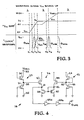
- Figs. 1-3 are a block diagram and timing diagrams, respectively. Specific circuitry for implementing the functions described in the block diagram will be presented with reference to Figs. 4, 5, and 6.
- the memory array 10 includes an N-well 12 and DRAM memory logic circuitry 14.
- the N-well is coupled to the output of a well pump 16.
- the well pump has an input for receiving a well pump enable signal, ⁇ WPE , clocked by a well regulator 18.
- the well regulator 18 has an input coupled to the N-well for monitoring the N-well bias level, V w .
- the well pump enable signal, ⁇ WPE is directed to the input of a well detector enable circuit 20.
- a well detector enable circuit 20 clocks a well detector enable signal, ⁇ WDE .
- the well detector enable circuit includes a first input coupled to ⁇ WPE and a second input coupled to V w .
- This well detector enable signal, ⁇ WDE is directed to a first input of a well detector circuit 22.
- a second input of the well detector circuit 22 is coupled to the N-well 12 and monitors V w .
- the well detector 22 clocks a gate control signal, V WH .
- a NAND gate 24 receives the gate control signal, V WH , at a first input and receives the external control signal, RAS , at a second inverting input.
- the NAND gate 24 clocks the internal control signal, RAS (INT), which is coupled to the control input 26 of the DRAM memory logic circuitry 14.
- Fig. 2 is a timing diagram depicting the voltage levels, V cc and V w , as a function of time. Additionally, the states of the gate control signal, VWH, the internal control signal, RAS , the well detector enable signal, ⁇ WDE , and the well pump enable signal, ⁇ WPE are depicted.
- the external power supply is turned on and the external power supply voltage level begins to increase.
- the external voltage supply level is equal to the full value V cc .
- the well regulator clocks ⁇ WPE high whenever V well is less than a reference voltage equal to 1.5 V cc .
- ⁇ WPE is clocked high the well pump is enabled and transfers charge to the N-well to increase the bias voltage level, V w , of the well.
- the quantity V w increases more slowly than the external power supply voltage level because the capacitance of the N-well is high and a substantial amount of charge must be pumped in the N-well to increase V w to 1.5 V cc .
- V w is equal to 1.5 V CC and ⁇ WPE is clocked low by the voltage regulator 18. If V well is above 1.5 V cc then charge will be transferred from the well to the ground tunnel of the external power supply via the well regulator 18. Note that the well regulator 18, well pump 16, and N-well 12 are coupled to form a feedback loop to maintain the value of V w at 1.5 V CC .
- the well detector enable circuit 20 clocks ⁇ WDE high when ⁇ WPE is high and V W is less than V CC + V T , where-V T is the threshold voltage of a PMOS transistor.
- ⁇ WDE is clocked high
- the well detector circuit 22 is enabled.
- the signal ⁇ WDE is clocked low when V w is greater than V cc + V T .
- the well detector 22 is disabled when ⁇ WDE is clocked low. In Fig. 2 ⁇ WDE is clocked low at time T i .
- the well detector 22 clocks V WH to the low voltage state when V w is less than V cc and clocks V wH to the high voltage state at time T 2 when V w is greater than Vcc.
- V wH The function of the gate control signal, V wH , will now be described.
- Table 1 is a truth table for the NAND gate 24 with the inverting input. When V wH is low the external control signal,
- RAS (INT) is high regardless of the state of the external control signal
- the active state of the memory array 10 could be initiated during the period To to T2. If the active state were initiated during this time, the sense amps would pull half of the bit lines to V cc and the junction between those bit lines and the N-well would be forward biased, thereby inducing charge injection and bipolar latchup. Thus, when V w is less than V cc , the gate 24 prevents the external control signal, RAS , from affecting the value of RAS (INT) received at the control input 26. The voltage levels on the bit lines are maintained at V cc /2.
- V WH is clocked low to release the chip from the well detector 22 and make the gate 24 transparent to the RAS signal.
- RAS (INT) is equal to to RAS
- the well detector is a CMOS differential amplifier with the inverting input coupled to V cc and the non-inverting input coupled to V w .
- This amplifier draws current and dissipates power.
- the well detector 22 performs no useful function once V W is greater than V cc . Accordingly, the well detector enable circuit 20 clocks ⁇ WDE low at time T z when V w is equal to about V cc + V T . Thus the power dissipation of the system is minimized to preserve the inherent low power features of CMOS technology.
- V cc bumps from four volts to seven volt between time X, and time X 4 .
- V w is equal to 1.5 V cc
- V WH is low
- the NAND gate 24 is transparent
- RAS (IN T ) is equal to the state of RAS
- the chip is under the.control of the external control signal, RAS
- ⁇ WPE is clocked high because V w is less than 1.5 V cc . Clocking ⁇ WPE high enables the well pump 16.
- the well pump 16 begins transferring charge to the N-well to increase V w . As described above, the rate of increase of V w is less than the rate of increase of V cc due to N-well capacitance.
- V cc is greater than V w
- V wH is clocked low to set RAS (INT) high and force the chip into the precharge state.
- RAS has no effect on the state of the memory array.
- Vw is equal to V cc and the well detector clocks V WH high to release the chip and restore control of the chip to the external control signal, RAS
- the well detector enable circuit clocks ⁇ WDE low to disable the well detector and conserve power.
- V w is again equal to 1.5 V cc and ⁇ WPE is clocked low to disable the well pump 16.
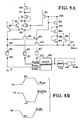
- Fig. 4 is a circuit diagram of the well regulator 18.
- the well regulator includes a biasing circuit 29 comprising first and second PMOS biasing transistors 30 and 31.
- the source terminal of the first biasing transistor 30 is coupled to a V w input 33, the gate is coupled to V cc , and the drain terminal is coupled to a biasing node 34.
- the source terminal of the second biasing transistor 31 is coupled to the biasing node 34, the gate is coupled to ground, and the drain terminal is coupled to ground 35.
- the CMOS comparator 36 is formed by a first series circuit including a first input transistor 37 and NMOS transistor 38, and by a second series circuit including second input transistor 39 and NMOS transistor 40.
- the first input transistor 37 has its source terminal coupled to V cc , its gate coupled to the biasing node 34, and its drain terminal coupled to an output node 41.
- NMOS transistor 38 has its drain terminal coupled to output node 41 and its source terminal coupled to ground.
- the second input transistor 39 has its source terminal coupled to V cc , and its drain terminal coupled to circuit node 42.
- the gates of NMOS transistors 38 and 40 are coupled to circuit node 42.
- a reference circuit 43 includes PMOS transistor 44, having its source terminal coupled to V cc and its drain terminal and gate coupled to reference node 45 and PMOS transistor 46, having its source terminal coupled to reference node 45 and its drain terminal and gate coupled to ground.
- the output node 41 is coupled to a ⁇ PWPE terminal 47 by inverters 48a and b.
- the transistors 30 and 31 of the biasing circuit 29 each have the same (W/L) ratio.
- the voltage level at the biasing node 34 is greater than V cc /2 if V WELL is greater.than 1.5 V cc and less than V cc /2, if V WELL is less than 1.5 V cc .
- the input voltage, V,, at the gate of the first input transistor 37 of the CMOS comparator 36 is coupled to the biasing node 34. Accordingly, V, is greater than V2 if V WELL is greater than 1.5 V cc and V, is less than V 2 if V WELL is less than 1.5 Vcc.
- V is greater than V2 then the voltage level on the output node 41 is low and if V, is less than V 2 then the voltage level on the output node 41 is high.
- the voltage level on ⁇ WPE terminal 47 is the same as the voltage level on the output node 41. Accordingly, the well regulator circuit 18 clocks ⁇ WPE high when V WELL is less than 1.5 Vcc and clocks ⁇ WPE low when VWELL is greater than 1.5 Vcc.
- FIG. 5A A circuit diagram of the charge pump 16 is depicted in Figs. 5A and 5B.
- Fig. 5C is a phase diagram of the clock signals utilizing the circuit pump.
- a NAND gate 48 has a first input coupled to the ⁇ WPE terminal 47.
- the output of the NAND gate 48 is coupled to the input of the delay 49 with the output of the delay 49 coupled to a second input of NAND gate 48.
- the output of the delay 49 is coupled to the input of a clock generator 50.
- Clock generator 50 provides clock outputs ⁇ WP1 , ⁇ WP2B and ⁇ WP2 at clock outputs 51, 52, 53, respectively.
- Clock generator output 53 is coupled to a first circuit node 54 by depletion device 55, clock generator output terminal 52 is coupled to a second circuit node 56 via capacitor 57, and clock generator terminal 51 is coupled to a third circuit node 58 by capacitor 60.
- the voltage level on the first circuit node 54 is designated V A , on the second circuit node 56 V B , and on the third circuit node 58 V c .
- the first circuit node 54 is coupled to a V WELL output terminal 62 by NMOS transistor 64.
- the first terminal 54 is coupled to the second terminal 56 by NMOS transistor 66.
- the first circuit node 54 is coupled to V cc by NMOS transistor 68.
- the gates of transistors 66 and 68 are coupled to the third circuit node 58.
- the gate of transistor 64 is coupled to the second circuit node 56.
- NMOS ransistor 70 has one terminal coupled to the third node 58, a second terminal coupled to V cc , and its gate coupled to V cc .
- Transistor 72 has a first terminal coupled to the third node 58 and a second terminal coupled to node 74. Node 74 is coupled to the first terminal of transistor 76 and to the gate of transistor 76. A second terminal of transistor 76 is coupled to circuit node 78. Circuit node 78 is coupled to a first terminal of transistor 80 and to the gate of transsistor 80. The second terminal of transistor 80 is coupled to V cc .
- the gate of transistor 72 is coupled to the third node 58 . and to V cc by NMOS transistor 82.
- NMOS Transistor 84 has one terminal coupled to the V WELL terminal 62 and a second terminal coupled to circuit node 86 and has its gate also coupled to circuit node 86.
- NMOS transistor 88 has a first terminal coupled to node 86, a second terminal coupled to node 90 and has its gate also being coupled to node 90.
- NMOS transistor 92 has a first terminal connected to node. 90, a second terminal connected to node 94.
- Node 94 is coupled to the gates of transistors 82 and 92 and also to the second circuit node 56.
- the V WELL terminal 62 is coupled to V cc by NMOS transistor 96.
- the gate of transistor 96 is also coupled to V cc .
- Fig. 5B is a timing diagram of the output signals from the clock generator 50. The operation of the charge pump will now be described with reference to Fig. 5B.
- the first circuit node 54 is coupled to the V WELL output terminal 62 because ⁇ WP2B is high and transistor 64 is conducting.
- the first circuit node is isolated from the V cc terminat because ⁇ WP1 is low and transistor 68 is not conducting.
- the first circuit node 54 is isolated from the V WELL terminal 62 because ⁇ WP2B is clocked low and transistor 64 is off.
- the voltage level V c on the third node 58, is clocked from the low state to the high state by ⁇ WP1. Accordingly, transistors 66 and 68 are switched on and the first and second nodes 54 and 56 are charged to Vcc.
- ⁇ WP1 is clocked low to switch off transistors 66 and 68 and isolate the first and second circuit nodes 54 and 56 from V cc .
- WP2 is clocked high and, because V A has been precharged to V cc during time period II, VA is boosted to about 10 volts. Additionally, 0 WP2B is also clocked high and the voltage level V B is boosted to about 10 volts. Because the second node is high, transistor 64 is switched on and the first node is coupled to the V WELL terminal 62. The excess charge pumped into the first circuit node 54 by the 0 signal is transferred to the well to increase V WELL . This pumping continues until ⁇ WPE is clocked low by the well detector. Accordingly, the charge pump increases V WELL to 1.5 V c c.
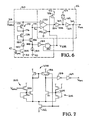
- Fig. 6 is a circuit diagram depicting circuitry for the well detector 22 and the well detector enabling circuit 20.
- the well detector 22 includes a CMOS differential amplifier 50 having its inverting input coupled to V cc terminal 40 and its non-inverting input coupled to V w terminal 34.
- the differential amplifier 150 is coupled to the ground terminal 40 of the power supply via NMOS disabling transistor 152.
- the gate of the disabling transistor 152 receives the ⁇ WDE signal.
- the output of the differential amplifier 150 is coupled to a holding node 154.
- a PMOS holding transistor 156 has its source terminal coupled to V cc terminal 44, its gate coupled too WDE and its drain terminal coupled to a holding node 154.
- Inverter 158 has its input coupled to holding node 154 and its output coupled to circuit node 160.
- Circuit node 160 is coupled to the V cc terminal 44 by capacitor 162.
- Inverter 164 has its input coupled to circuit node 160 and its output coupled to a well detector output terminal 166.
- the well detector enabling circuit 20 includes a detection circuit 170, including a first PMOS detection transistor 172, having its source terminal coupled to the V w terminal 34, its drain terminal coupled to a circuit node 176, and its gate coupled to circuit node 176.
- Second detection transistor 178 has its source terminal coupled to node 176, its drain terminal coupled to circuit node 180, and its gate coupled to circuit node 180.
- Circuit node 180 is coupled to a CMOS current source 182.
- the current source 182 is coupled to the ground terminal 40 by NMOS transistor 184.
- NMOS transistor 184 has its gate coupled to the ⁇ WPE signal.
- a PMOS output transistor 186 has its source terminal connected to the V cc terminal 44, its drain terminal coupled to an output node 188, and its gate coupled to circuit node 180.
- the output node 188 is coupled to the ground terminal 40 by a CMOS current source 190.
- Output terminal 188 is coupled to a first input of a well detector NAND gate 192 via inverter 194.
- the second input of the NAND gate 192 is coupled to the output terminal 166 of the well detector 22.
- the output of NAND gate 192 is coupled to the gate of the disabling transistor 152 and provides the the 0 WDE signal.
- the detection circuit 170 is activated when ⁇ WDE is clocked high and NMOS transistor 184 conducts. Circuit node 180 is pulled low, thereby creating a negative potential at the gate of the second detection transistor 178.
- the second detection transistor 178 is connected in the diode configuration, i.e., the gate is coupled to the drain. When V Gs of transistor 178 is equal to -V T , transistor 178 conducts and pulls node 176 low. Similarly, when node 176 is pulled low the first detection transistor 172 begins to conduct. Because both the detection transistors 172 and 178 are coupled in the diode configuration the voltage level at node 176 is equal to V w -V T and the voltage level at node 180 is equal to V w -2V T .
- V G of transistor 186 is equal to Vw -2V T .
- output transistor 186 conducts when V GS is equal to -V T or when V w is less than or equal to V cc + V T .
- the output transistor 186 conducts the output node 188 is charged to V cc .
- Table 2 is a truth table for the well detector enable NAND gate 192, where V o is the voltage level at the output node 188.
- V WH acts as a gate control signal for the well detector enable NAND gate 192.
- V WH is low, i.e., when the array is forced into precharge, ⁇ WDE is always high and the well detector 22 is always enabled.
- V WH is high, i.e., the array is released, the state of ⁇ WDE is the same as the state of V o .
- V w is less than 1.5 V cc
- ⁇ WPE is clocked high by the well regulator. Accordingly, the detection circuit 170 of the well detector enable circuit 20 is activated by transistor 184. The signal V o is clocked high because V w is less than V cc , and V T and the output transistor 186 conducts to charge the output node 188. V WH is still high because node 154 is coupled to node V cc by the PMOS transistor 156. Thus, from the Table 2, with V a high and V WH high, ⁇ WDE is clocked high and the disabling transistor 152 conducts to enable the difference amplifier 150.
- V WH remains high.
- V w is less than V cc , so that the output of the difference amplifier 150 is low and V WH remains low. Additionally, V o is high because V w is less than V cc + V T . From Table 2, ⁇ WDE remains high and the differential amplifier 150 continues to be enabled and hold WH low.
- V w is greater than V cc but less than V cc + V T .
- V WH is clocked high by the difference amplifier 150 because V w is greater than V cc .
- V o still remains low because V w is less than V cc + V T . Accordingly, V WDE is still high and the differential amplifier 150 remains enabled during this short time period to charge the holding capacitor 162 to hold V wH high during the transition period when the difference amplifier 150 is disabled.
- V w is greater than V cc + V T , the output transistor 186 is deactivated, and the output node 188 is discharged via the current source 190. Accordingly, V o goes low. From Table 2, with V o low and V WH high, ⁇ WDE is clocked low to turn off the disabling transistor 152 and disable the differential amplifier 150. The V WH signal is held high by capacitor 162 while the ⁇ WDE signal activates holding transistor 156 to charge the holding node 154 high and hold V WH at the high voltage level.
- Fig. 7 is a circuit diagram of CMOS differential amplifier 150.
- the + input is + node 200 of input circuit 202.
- the -input is -node 204 of reference circuit 206.
- a CMOS comparator 208 provides a high output at output node 154 when V + >V. and a low output when V + ⁇ V-The voltage level at -node 204 is set at V cc /2 by reference circuit 206.
- the voltage level at + node 200 is set at V WELL /2 by input circuit 202. ' Accordingly, the voltage level, V WH , at output node 154 is high when V w >V cc and low when V w ⁇ V cc .
- the present invention thus prevents forward biasing of junctions between the bit lines and transfer gates and N-well to prevent charge injection or bipolar latchup during the active cycle of the memory.
- the well detector enabling circuit reduces power dissipation by disabling the well detector when it is not needed.
- the invention has been explained with reference to specific embodiments. Other embodiments will now be apparent to those of ordinary skill in the art.
- the invention may be utilized in a memory array having NMOS bit line connections and transfer gates disposed in a P-type well.
- other gating configurations than those described above may be utilized to attain the equivalent logical functions described herein.
- the states of the various signals set forth above may be varied by utilizing inverters.
- the techniques described for controlling the states of the well pump enabling signal, well detector enabling signal, and gate control signals may be utilized in other technologies, such as NMOS, PMOS, or bipolar. Accordingly, it is therefore not intend that the invention be limited except as indicated by the appended claims.
Abstract
Description
- The invention relates generally to memory arrays and in particular to biasing a region in a semiconductor integrated circuit to a selected voltage level and, more particularly, to a system for preventing undesired charge injection for bipolar latchup in a integrated circuit.
- Recent advances in CMOS technology have allowed memory circuit designers to realize the power reduction inherent in CMOS design while achieving high density. However, as memory cell size decreases to allow for high density arrays, the susceptibility of alpha particle induced soft errors in the array increases. A CMOS DRAM utilizing PMOS memory cells disposed in an N-well formed in P substrate significantly reduces this soft error susceptibility.
- The N-well must be biased to a higher voltage level than the PMOS transfer gates in the memory cells and the P channel bit line connections to reverse bias the semiconductor junctions formed between these PMOS elements and the N-well. If these junctions are forward biased, then undesired charge injection takes place between the PMOS memory cells and the bit line connections in the N-well, thereby destroying the information stored in the memory. Additionally, the various P type and N type regions in a CMOS array form bipolar transistors. If the above-described junctions are forward biased then the transistors may form a feedback current loop to allow high substrate current. This phenomenon is termed bipolar latchup.
- The active cycle of the memory is initiated by clocking a control signal received at a control input of the memory. During the active cycle, selected word lines are clocked to couple selected storage cells to the bit lines. The voltage level on half the bit lines in the array are pulled to the power supply level, Vcc, by the sense amps.
- The N-well may be biased to a multiple of Vcc, e.g., 1.5 Vcc, to prevent forward biasing during the active cycle. A CMOS memory having an N-well biased at 1.5 Vcc is described in an article by Shimohigashi, et al. entitled "An N-Well CMOS Dynamic RAM," IEEE Journal of Solid State Circuits, Vol. SC-17, No. 2, April, 1982, pp. 344-348.
- However, during initial power-up, or during an excursion in the value of the power supply voltage (Vcc bump), the bit line voltage may exceed the N-well bias voltage and forward bias the semiconductor junction. The large capacitance of the N-well causes the rate of change of the N-well bias voltage level to be slower than the rate of change of the bit line voltage level. Thus, the bit line voltage may exceed the N-well voltage for a'short time.
- During this time the above-described problems of charge injection and bipolar latchup will be present if the memory is in the active cycle. Accordingly, a system for preventing the forward biasing of the junctions between the bit lines and the N-well during the active cycle of the memory is greatly needed in the industry. This system must protect the memory during initial power-up and during a Vcc bump. Additionally, the system must consume low power so as not to degrade the low power dissipation inherent in CMOS technology.
- The present invention is a system for preventing forward biasing of the bit line junctions and memory cell junctions formed between the N-well and bit line terminals and memory cells, respectively. The system is for use with a memory array where the bit lines are precharged to a fraction of Vcc, e.g., Vcc/2.
- The invention includes a gating system for forcing the array into precharge during a critical time period when Vw is less than V cc. The gating system overrides the external control signal during the critical period. Thus, the bit line held at Vcc/2 until Vw is greater than Vcc.
- According to a further aspect of the invention, a well regulator and charge pump maintain Vw at a multiple of Vcc, e.g., 1.5 Vcc. However, during initial powerup or a Vcc bump Vw rises more slowly than Vccbecause of the large capacitance of the well. Accordingly, Vw will be less than Vcc during a critical time period.
- If the array were driven into the active cycle during this critical time period, then half the bit lines would be pulled to Vcc. Because Vw is less than Vcc, the junctions between these bit lines and the N-well would be forward biased, thereby causing charge injection and bipolar latchup.
- The gating system prevents forward biasing during the critical period by holding the array in precharge to maintain the bit line voltage at
V cd2. Once Vw is greater than Vcc the gating system releases the array to the control of the extemal control signal. - In a preferred embodiment, the gate control signal is clocked by a CMOS differential amplifier having its inverting input coupled to Vcc and its non-inverting input coupled to Vw .
- According to a further aspect of the invention, a well enabling circuit clocks a well enabling signal to disable the differential amplifier when Vw is greater than Vcc + VT, where VT is the threshold of a MOS transistor.
- According to a further aspect of the invention, a holding transistor holds the gate control signal at Vcc when the well detector is disabled.
- The differential amplifier consumes power when in operation. By disabling the differential amplifier subsequent to termination of the critical time period, power dissipation of the system is reduced.
- Other aspects and advantages will become apparent by reference to the drawings and the detailed description which follow.
-
- Fig. 1 is a block diagram of an embodiment of the invention.
- Fig. 2 is a timing diagram indicating the state of the various control signals and voltage levels during the powerup phase of memory operation.
- Fig. 3 is a timing diagram indicating the state of the various control signals and voltage levels during a power supply excursion.
- Fig. 4 is a circuit diagram of the well regulator.
- Fig. 5A is a circuit diagram of a charge pump.
- Fig. 5B is a timing diagram of the clock signals utilized in the circuit of Fig. 5A.
- Fig. 6 is a schematic diagram of the well detector and well detector enabling circuits.
- Fig. 7 is a circuit diagram of the well detector.
- The present invention is a system for preventing charge injection from the bit lines to the N-well and for preventing bipolar latchup during the active cycle of a CMOS memory array. The system is for use in a memory scheme where the bit lines are biased to V cc/2 during the precharge cycle of the memory. A biasing system suitable for use with the present invention is disclosed in the copending, commonly assigned, patent application entitled "CMOS DRAM MEMORY ARRAY BIAS SCHEME," attorney docket No. A301, by Chuang, et al. There, an externally clocked signal,
RAS , is received at the control input of the memory. When - is high the chip is in the precharge state and the bit lines are coupled to each other and to a Vcc/2 bias voltage generator. When
RAS . is clocked low, the bit lines are isolated from each other and from the Vcc/2 bias voltage generator. - During the active cycle, half of the bit lines in the array are pulled to Vcc and half are pulled to ground by the sense amplifiers. When
-
RAS is clocked high again, the bit lines are again coupled to each other and to the V cc/2 bias voltage generator to rapidly return the bit lines to Vcc/2. - In the description that follows, various control signals are switched between low and high voltage states in response to specified circuit conditions. Generally, the magnitude of the high voltage state is equal to about Vcc and the magnitude of the low - voltage state is equal to about ground.
- The operation of the circuit will be generally described with reference to Figs. 1-3, which are a block diagram and timing diagrams, respectively. Specific circuitry for implementing the functions described in the block diagram will be presented with reference to Figs. 4, 5, and 6.
- Referring now to Fig. 1, the memory array 10 includes an N-
well 12 and DRAMmemory logic circuitry 14. The N-well is coupled to the output of awell pump 16. The well pump has an input for receiving a well pump enable signal, ØWPE, clocked by awell regulator 18. - The
well regulator 18 has an input coupled to the N-well for monitoring the N-well bias level, Vw. The well pump enable signal, ØWPE, is directed to the input of a well detector enablecircuit 20. - A well detector enable
circuit 20 clocks a well detector enable signal, ØWDE. The well detector enable circuit includes a first input coupled to ØWPE and a second input coupled to Vw. - This well detector enable signal, ØWDE, is directed to a first input of a
well detector circuit 22. A second input of thewell detector circuit 22 is coupled to the N-well 12 and monitors Vw. Thewell detector 22 clocks a gate control signal, VWH. - A
NAND gate 24 receives the gate control signal, VWH, at a first input and receives the external control signal,RAS , at a second inverting input. TheNAND gate 24 clocks the internal control signal,RAS (INT), which is coupled to thecontrol input 26 of the DRAMmemory logic circuitry 14. - The operation of the circuit depicted in Fig. 1 will now be described with reference to Fig. 2. Fig. 2 is a timing diagram depicting the voltage levels, Vccand Vw, as a function of time. Additionally, the states of the gate control signal, VWH, the internal control signal,
RAS , the well detector enable signal, ØWDE , and the well pump enable signal, ØWPE are depicted. - Referring now to Fig. 2, at time To the external power supply is turned on and the external power supply voltage level begins to increase. At time T, the external voltage supply level is equal to the full value Vcc. Note that the bias voltage level of the N-well 12 increases more slowly than the external power supply voltage. The well regulator clocks ØWPE high whenever V well is less than a reference voltage equal to 1.5 Vcc. When ØWPE is clocked high the well pump is enabled and transfers charge to the N-well to increase the bias voltage level, Vw, of the well. The quantity Vw increases more slowly than the external power supply voltage level because the capacitance of the N-well is high and a substantial amount of charge must be pumped in the N-well to increase Vw to 1.5 V cc.
- At time T4, Vw is equal to 1.5 VCC and ØWPEis clocked low by the
voltage regulator 18. If V well is above 1.5 Vcc then charge will be transferred from the well to the ground tunnel of the external power supply via thewell regulator 18. Note that thewell regulator 18, well pump 16, and N-well 12 are coupled to form a feedback loop to maintain the value of Vw at 1.5 VCC. - The well detector enable
circuit 20 clocks ØWDE high when ØWPE is high and VW is less than VCC + V T, where-VT is the threshold voltage of a PMOS transistor. When φWDE is clocked high, thewell detector circuit 22 is enabled. The signal φWDE is clocked low when Vw is greater than Vcc + VT. Thewell detector 22 is disabled when φWDE is clocked low. In Fig. 2 φWDEis clocked low at time Ti. - The
well detector 22 clocks VWH to the low voltage state when V w is less than Vcc and clocks VwHto the high voltage state at time T2 when Vw is greater than Vcc. - The function of the gate control signal, V wH, will now be described. Table 1 is a truth table for the
NAND gate 24 with the inverting input. When VwH is low the external control signal, -
RAS (INT), is high regardless of the state of the external control signal, -
AAS . Thus, when Vw is less than Vcc,RRS (INT) is always in the high voltage state and the chip is always in the precharge state. As described above, during the precharge state the bit lines are biased to Vcc/2. -

- If the external control signal,
RAS , were directly connected to the memoryarray control input 26, then the active state of the memory array 10 could be initiated during the period To to T2. If the active state were initiated during this time, the sense amps would pull half of the bit lines to Vcc and the junction between those bit lines and the N-well would be forward biased, thereby inducing charge injection and bipolar latchup. Thus, when Vw is less than Vcc, thegate 24 prevents the external control signal,RAS , from affecting the value ofRAS (INT) received at thecontrol input 26. The voltage levels on the bit lines are maintained at Vcc/2. - When the well bias level, Vw, increases to Vcc, then VWH is clocked low to release the chip from the
well detector 22 and make thegate 24 transparent to theRAS signal. Referring back to Table 1, when VWH is high, -
RAS (INT) is equal to toRAS - As will be described more fully below, the well detector is a CMOS differential amplifier with the inverting input coupled to Vcc and the non-inverting input coupled to Vw. This amplifier draws current and dissipates power. The
well detector 22 performs no useful function once VW is greater than Vcc . Accordingly, the well detector enablecircuit 20 clocks φWDE low at time Tz when Vw is equal to about Vcc + VT. Thus the power dissipation of the system is minimized to preserve the inherent low power features of CMOS technology. - The functioning of the system during a Vccbump will now be described with reference to the timing diagram of Fig. 3. In Fig. 3, Vcc bumps from four volts to seven volt between time X, and time X4.
- At time X,, Vw is equal to 1.5 Vcc, VWH is low, the
NAND gate 24 is transparent, and the state of -
RAS (INT) is equal to the state ofRAS Thus, the chip is under the.control of the external control signal,RAS - At time X2, φWPE is clocked high because Vw is less than 1.5 Vcc. Clocking φWPE high enables the
well pump 16. Thewell pump 16 begins transferring charge to the N-well to increase Vw. As described above, the rate of increase of Vw is less than the rate of increase of Vcc due to N-well capacitance. - At time X3, Vcc is greater than Vw, and VwHis clocked low to set
RAS (INT) high and force the chip into the precharge state. At this point, the external control signal,RAS has no effect on the state of the memory array. - The magnitude of Vw continues to increase due to the action of the charge pump and, at time Xs, Vw is equal to Vcc and the well detector clocks VWH high to release the chip and restore control of the chip to the external control signal,
RAS - At time X6, the well detector enable circuit clocks φWDE low to disable the well detector and conserve power. At time X,, Vw is again equal to 1.5 Vcc and φWPE is clocked low to disable the
well pump 16. - Fig. 4 is a circuit diagram of the
well regulator 18. The well regulator includes a biasingcircuit 29 comprising first and secondPMOS biasing transistors 30 and 31. The source terminal of thefirst biasing transistor 30 is coupled to a Vw input 33, the gate is coupled to Vcc, and the drain terminal is coupled to a biasingnode 34. The source terminal of the second biasing transistor 31 is coupled to the biasingnode 34, the gate is coupled to ground, and the drain terminal is coupled toground 35. - The
CMOS comparator 36 is formed by a first series circuit including afirst input transistor 37 andNMOS transistor 38, and by a second series circuit includingsecond input transistor 39 andNMOS transistor 40. Thefirst input transistor 37 has its source terminal coupled to Vcc, its gate coupled to the biasingnode 34, and its drain terminal coupled to anoutput node 41.NMOS transistor 38 has its drain terminal coupled tooutput node 41 and its source terminal coupled to ground. Thesecond input transistor 39 has its source terminal coupled to Vcc, and its drain terminal coupled tocircuit node 42. The gates ofNMOS transistors circuit node 42. - A
reference circuit 43 includesPMOS transistor 44, having its source terminal coupled to Vcc and its drain terminal and gate coupled toreference node 45 and PMOS transistor 46, having its source terminal coupled toreference node 45 and its drain terminal and gate coupled to ground. - The
output node 41 is coupled to a φPWPEterminal 47 by inverters 48a and b. - The operation of the circuit depicted in Fig. 4 will now be described. The (W/L) ratios of
transistors 44 and 46 in thereference circuit 43 are equal so that the voltage level at thereference node 45 is Vcc/2. Accordingly, the input voltage, V2, at the gate of thesecond input transistor 39 of theCMOS comparator 36 is set at Vcc/2. - The
transistors 30 and 31 of the biasingcircuit 29 each have the same (W/L) ratio. The voltage level at the biasingnode 34 is greater than Vcc/2 if VWELL is greater.than 1.5 Vcc and less than Vcc/2, if VWELL is less than 1.5 Vcc. The input voltage, V,, at the gate of thefirst input transistor 37 of theCMOS comparator 36 is coupled to the biasingnode 34. Accordingly, V, is greater than V2 if VWELL is greater than 1.5 Vcc and V, is less than V2 if VWELL is less than 1.5 Vcc. - If V, is greater than V2 then the voltage level on the
output node 41 is low and if V, is less than V2 then the voltage level on theoutput node 41 is high. The voltage level onφWPE terminal 47 is the same as the voltage level on theoutput node 41. Accordingly, thewell regulator circuit 18 clocks φWPE high when VWELL is less than 1.5 Vcc and clocks φWPElow when VWELL is greater than 1.5 Vcc. - A circuit diagram of the
charge pump 16 is depicted in Figs. 5A and 5B. Fig. 5C is a phase diagram of the clock signals utilizing the circuit pump. Referring now to Fig. 5A, aNAND gate 48 has a first input coupled to the φWPE terminal 47. The output of theNAND gate 48 is coupled to the input of the delay 49 with the output of the delay 49 coupled to a second input ofNAND gate 48. The output of the delay 49 is coupled to the input of aclock generator 50.Clock generator 50 provides clock outputs φWP1, φWP2B and φWP2 at clock outputs 51, 52, 53, respectively. -
Clock generator output 53 is coupled to afirst circuit node 54 bydepletion device 55, clockgenerator output terminal 52 is coupled to asecond circuit node 56 viacapacitor 57, andclock generator terminal 51 is coupled to a third circuit node 58 by capacitor 60. The voltage level on thefirst circuit node 54 is designated VA, on the second circuit node 56 VB, and on the third circuit node 58 Vc. - The
first circuit node 54 is coupled to a VWELL output terminal 62 byNMOS transistor 64. Thefirst terminal 54 is coupled to thesecond terminal 56 byNMOS transistor 66. Thefirst circuit node 54 is coupled to Vcc byNMOS transistor 68. The gates oftransistors transistor 64 is coupled to thesecond circuit node 56. - NMOS ransistor 70 has one terminal coupled to the third node 58, a second terminal coupled to Vcc, and its gate coupled to Vcc. Transistor 72 has a first terminal coupled to the third node 58 and a second terminal coupled to node 74. Node 74 is coupled to the first terminal of
transistor 76 and to the gate oftransistor 76. A second terminal oftransistor 76 is coupled to circuit node 78. Circuit node 78 is coupled to a first terminal oftransistor 80 and to the gate oftranssistor 80. The second terminal oftransistor 80 is coupled to Vcc. The gate oftransistor 72 is coupled to the third node 58 . and to Vcc byNMOS transistor 82. - NMOS Transistor 84 has one terminal coupled to the VWELL terminal 62 and a second terminal coupled to circuit node 86 and has its gate also coupled to circuit node 86.
NMOS transistor 88 has a first terminal coupled to node 86, a second terminal coupled to node 90 and has its gate also being coupled to node 90.NMOS transistor 92 has a first terminal connected to node. 90, a second terminal connected tonode 94.Node 94 is coupled to the gates oftransistors second circuit node 56. The VWELL terminal 62 is coupled to Vcc by NMOS transistor 96. The gate of transistor 96 is also coupled to Vcc. - Fig. 5B is a timing diagram of the output signals from the
clock generator 50. The operation of the charge pump will now be described with reference to Fig. 5B. During time period I thefirst circuit node 54 is coupled to the VWELL output terminal 62 because φWP2B is high andtransistor 64 is conducting. The first circuit node is isolated from the Vccterminat because φWP1 is low andtransistor 68 is not conducting. - During time period II the
first circuit node 54 is isolated from the V WELL terminal 62 because φWP2B is clocked low andtransistor 64 is off. The voltage level Vc, on the third node 58, is clocked from the low state to the high state by φWP1. Accordingly,transistors second nodes - During time period III, φWP1 is clocked low to switch off
transistors second circuit nodes WP2 is clocked high and, because VA has been precharged to Vcc during time period II, VA is boosted to about 10 volts. Additionally, 0WP2B is also clocked high and the voltage level VB is boosted to about 10 volts. Because the second node is high,transistor 64 is switched on and the first node is coupled to the VWELLterminal 62. The excess charge pumped into thefirst circuit node 54 by the 0 signal is transferred to the well to increase VWELL. This pumping continues until φWPE is clocked low by the well detector. Accordingly, the charge pump increases VWELL to 1.5 Vcc. - Fig. 6 is a circuit diagram depicting circuitry for the
well detector 22 and the welldetector enabling circuit 20. Thewell detector 22 includes aCMOS differential amplifier 50 having its inverting input coupled to Vcc terminal 40 and its non-inverting input coupled to Vw terminal 34. Thedifferential amplifier 150 is coupled to theground terminal 40 of the power supply viaNMOS disabling transistor 152. The gate of the disablingtransistor 152 receives the φ WDE signal. The output of thedifferential amplifier 150 is coupled to a holdingnode 154. APMOS holding transistor 156 has its source terminal coupled to Vcc terminal 44, its gate coupled tooWDE and its drain terminal coupled to a holdingnode 154.Inverter 158 has its input coupled to holdingnode 154 and its output coupled tocircuit node 160.Circuit node 160 is coupled to the Vcc terminal 44 bycapacitor 162.Inverter 164 has its input coupled tocircuit node 160 and its output coupled to a welldetector output terminal 166. - The well
detector enabling circuit 20 includes adetection circuit 170, including a firstPMOS detection transistor 172, having its source terminal coupled to the Vw terminal 34, its drain terminal coupled to acircuit node 176, and its gate coupled tocircuit node 176.Second detection transistor 178 has its source terminal coupled tonode 176, its drain terminal coupled tocircuit node 180, and its gate coupled tocircuit node 180.Circuit node 180 is coupled to a CMOS current source 182. The current source 182 is coupled to theground terminal 40 by NMOS transistor 184. NMOS transistor 184 has its gate coupled to the φWPE signal. - A PMOS output transistor 186 has its source terminal connected to the Vcc terminal 44, its drain terminal coupled to an
output node 188, and its gate coupled tocircuit node 180. Theoutput node 188 is coupled to theground terminal 40 by a CMOS current source 190. -
Output terminal 188 is coupled to a first input of a welldetector NAND gate 192 viainverter 194. The second input of theNAND gate 192 is coupled to theoutput terminal 166 of thewell detector 22. The output ofNAND gate 192 is coupled to the gate of the disablingtransistor 152 and provides the the 0WDE signal. - The
detection circuit 170 is activated when φWDE is clocked high and NMOS transistor 184 conducts.Circuit node 180 is pulled low, thereby creating a negative potential at the gate of thesecond detection transistor 178. Thesecond detection transistor 178 is connected in the diode configuration, i.e., the gate is coupled to the drain. When VGs oftransistor 178 is equal to -VT,transistor 178 conducts and pullsnode 176 low. Similarly, whennode 176 is pulled low thefirst detection transistor 172 begins to conduct. Because both thedetection transistors node 176 is equal to Vw -VT and the voltage level atnode 180 is equal to Vw -2VT . Because the gate of the output transistor 186 is coupled tonode 180, VG of transistor 186 is equal to Vw -2VT . Thus, output transistor 186 conducts when VGS is equal to -VT or when Vwis less than or equal to Vcc + VT. When the output transistor 186 conducts theoutput node 188 is charged to Vcc. - In summary, with φWPE clocked high, the voltage level at the
output node 188 is low when Vw is greater than Vcc + VT and is high when Vw is less than V cc + VT. Table 2 is a truth table for the well detector enableNAND gate 192, where Vo is the voltage level at theoutput node 188.
- From Table 2 it is apparent that VWH acts as a gate control signal for the well detector enable
NAND gate 192. When VWH is low, i.e., when the array is forced into precharge, φWDE is always high and thewell detector 22 is always enabled. However, when VWH is high, i.e., the array is released, the state of φWDE is the same as the state of Vo. - The voltage state of the φ
WDE signal will now be analyzed for the case of a voltage bump as illustrated in Fig. 3. At time X,, VWH is high and Vo is low because Vw is greater than V cc + VT. Accordingly, from Table 1, φ WDE is low, the disablingtransistor 152 is off, and thedifferential amplifier 150 is disabled. Thus, when the N-well is properly biased with respect to Vcc , thedifferential amplifier 150 is disabled to conserve power. - At time X2, Vw is less than 1.5 Vcc, and φWPEis clocked high by the well regulator. Accordingly, the
detection circuit 170 of the well detector enablecircuit 20 is activated by transistor 184. The signal Vo is clocked high because Vw is less than Vcc, and VT and the output transistor 186 conducts to charge theoutput node 188. VWH is still high becausenode 154 is coupled to node Vcc by thePMOS transistor 156. Thus, from the Table 2, with Va high and VWH high, φWDE is clocked high and the disablingtransistor 152 conducts to enable thedifference amplifier 150. Additionally, when φWDE is clocked high, the holdingtransistor 156 is deactivated to decouple the holdingnode 154 from the Vccterminal. The output of thedifference amplifier 150 is high because Vw is greater than V cc at time X2. Accordingly, VWH remains high. - At time X3 the output of the
differential amplifier 150 goes low because Vw is less than Vcc. Accordingly, VwH is clocked low and RAS - (INT) is held high to force the array into the precharge state. From Table 2, φWDE remains high and thedifferential amplifier 150 remains enabled. - During the period from X4 to Xs, Vw is less than Vcc, so that the output of the
difference amplifier 150 is low and VWH remains low. Additionally, Vo is high because Vw is less than Vcc + VT. From Table 2, φWDE remains high and thedifferential amplifier 150 continues to be enabled and hold WH low. - Between X5 and X6, Vw is greater than Vcc but less than Vcc + VT. VWH is clocked high by the
difference amplifier 150 because Vw is greater than Vcc. Vo still remains low because Vw is less than Vcc + VT. Accordingly, VWDE is still high and thedifferential amplifier 150 remains enabled during this short time period to charge the holdingcapacitor 162 to hold VwHhigh during the transition period when thedifference amplifier 150 is disabled. - At time X6, Vw is greater than Vcc + VT, the output transistor 186 is deactivated, and the
output node 188 is discharged via the current source 190. Accordingly, Vo goes low. From Table 2, with Vo low and VWH high, φWDE is clocked low to turn off the disablingtransistor 152 and disable thedifferential amplifier 150. The VWH signal is held high bycapacitor 162 while the φWDE signal activates holdingtransistor 156 to charge the holdingnode 154 high and hold VWH at the high voltage level. - Fig. 7 is a circuit diagram of CMOS
differential amplifier 150. In Fig. 7, the + input is +node 200 ofinput circuit 202. The -input is -node 204 ofreference circuit 206. - A CMOS comparator 208 provides a high output at
output node 154 when V +>V. and a low output when V+<V-The voltage level at -node 204 is set at Vcc/2 byreference circuit 206. The voltage level at +node 200 is set at VWELL/2 byinput circuit 202. ' Accordingly, the voltage level, VWH, atoutput node 154 is high when Vw>Vcc and low when Vw<Vcc. - The present invention thus prevents forward biasing of junctions between the bit lines and transfer gates and N-well to prevent charge injection or bipolar latchup during the active cycle of the memory. The well detector enabling circuit reduces power dissipation by disabling the well detector when it is not needed.
- The invention has been explained with reference to specific embodiments. Other embodiments will now be apparent to those of ordinary skill in the art. In particular, the invention may be utilized in a memory array having NMOS bit line connections and transfer gates disposed in a P-type well. Additionally, other gating configurations than those described above may be utilized to attain the equivalent logical functions described herein. Further, the states of the various signals set forth above may be varied by utilizing inverters. The techniques described for controlling the states of the well pump enabling signal, well detector enabling signal, and gate control signals may be utilized in other technologies, such as NMOS, PMOS, or bipolar. Accordingly, it is therefore not intend that the invention be limited except as indicated by the appended claims.
Claims (10)
Applications Claiming Priority (2)
| Application Number | Priority Date | Filing Date | Title |
|---|---|---|---|
| US747520 | 1985-06-21 | ||
| US06/747,520 US4670861A (en) | 1985-06-21 | 1985-06-21 | CMOS N-well bias generator and gating system |
Publications (2)
| Publication Number | Publication Date |
|---|---|
| EP0206785A2 true EP0206785A2 (en) | 1986-12-30 |
| EP0206785A3 EP0206785A3 (en) | 1990-01-17 |
Family
ID=25005416
Family Applications (1)
| Application Number | Title | Priority Date | Filing Date |
|---|---|---|---|
| EP86304775A Withdrawn EP0206785A3 (en) | 1985-06-21 | 1986-06-20 | Memory array |
Country Status (3)
| Country | Link |
|---|---|
| US (1) | US4670861A (en) |
| EP (1) | EP0206785A3 (en) |
| JP (1) | JPS61294698A (en) |
Cited By (3)
| Publication number | Priority date | Publication date | Assignee | Title |
|---|---|---|---|---|
| US4918663A (en) * | 1987-09-16 | 1990-04-17 | Motorola, Inc. | Latch-up control for a CMOS memory with a pumped well |
| GB2314698A (en) * | 1996-06-27 | 1998-01-07 | Hyundai Electronics Ind | Charge pump circuit |
| GB2323952A (en) * | 1997-04-02 | 1998-10-07 | Lg Semicon Co Ltd | Charge pump circuit for a semiconductor memory device |
Families Citing this family (22)
| Publication number | Priority date | Publication date | Assignee | Title |
|---|---|---|---|---|
| JPS6159688A (en) * | 1984-08-31 | 1986-03-27 | Hitachi Ltd | Semiconductor integrated circuit device |
| US4769784A (en) * | 1986-08-19 | 1988-09-06 | Advanced Micro Devices, Inc. | Capacitor-plate bias generator for CMOS DRAM memories |
| US5032892A (en) * | 1988-05-31 | 1991-07-16 | Micron Technology, Inc. | Depletion mode chip decoupling capacitor |
| GB9007791D0 (en) | 1990-04-06 | 1990-06-06 | Foss Richard C | High voltage boosted wordline supply charge pump and regulator for dram |
| GB9007790D0 (en) * | 1990-04-06 | 1990-06-06 | Lines Valerie L | Dynamic memory wordline driver scheme |
| US5063304A (en) * | 1990-04-27 | 1991-11-05 | Texas Instruments Incorporated | Integrated circuit with improved on-chip power supply control |
| KR930008886B1 (en) * | 1991-08-19 | 1993-09-16 | 삼성전자 주식회사 | Power supply circuit doing electrical programmable |
| KR940008286B1 (en) * | 1991-08-19 | 1994-09-09 | 삼성전자 주식회사 | Internal voltage-source generating circuit |
| US5268871A (en) * | 1991-10-03 | 1993-12-07 | International Business Machines Corporation | Power supply tracking regulator for a memory array |
| US5321647A (en) * | 1992-05-07 | 1994-06-14 | International Business Machines Corp. | Semiconductor memory device and operational method with reduced well noise |
| US5387826A (en) * | 1993-02-10 | 1995-02-07 | National Semiconductor Corporation | Overvoltage protection against charge leakage in an output driver |
| US5338978A (en) * | 1993-02-10 | 1994-08-16 | National Semiconductor Corporation | Full swing power down buffer circuit with multiple power supply isolation |
| US5381061A (en) * | 1993-03-02 | 1995-01-10 | National Semiconductor Corporation | Overvoltage tolerant output buffer circuit |
| JP3500149B2 (en) * | 1993-06-07 | 2004-02-23 | ナショナル・セミコンダクター・コーポレイション | Overvoltage protection |
| US5406140A (en) * | 1993-06-07 | 1995-04-11 | National Semiconductor Corporation | Voltage translation and overvoltage protection |
| US6344959B1 (en) | 1998-05-01 | 2002-02-05 | Unitrode Corporation | Method for sensing the output voltage of a charge pump circuit without applying a load to the output stage |
| US6448841B1 (en) | 1998-05-01 | 2002-09-10 | Texas Instruments Incorporated | Efficiency charge pump circuit |
| GB2343069B (en) * | 1998-06-30 | 2003-11-05 | Sgs Thomson Microelectronics | An on-chip higher-to-lower voltage input stage |
| US7642835B1 (en) * | 2003-11-12 | 2010-01-05 | Robert Fu | System for substrate potential regulation during power-up in integrated circuits |
| US6970031B1 (en) | 2004-05-28 | 2005-11-29 | Hewlett-Packard Development Company, L.P. | Method and apparatus for reducing charge injection in control of MEMS electrostatic actuator array |
| US7372748B2 (en) * | 2006-10-16 | 2008-05-13 | Sandisk Corporation | Voltage regulator in a non-volatile memory device |
| US7586322B1 (en) | 2007-05-02 | 2009-09-08 | Altera Corporation | Test structure and method for measuring mismatch and well proximity effects |
Citations (1)
| Publication number | Priority date | Publication date | Assignee | Title |
|---|---|---|---|---|
| GB1523564A (en) * | 1976-02-09 | 1978-09-06 | Nippon Electric Co | Memory circuit with protection circuit |
Family Cites Families (4)
| Publication number | Priority date | Publication date | Assignee | Title |
|---|---|---|---|---|
| JPS5472691A (en) * | 1977-11-21 | 1979-06-11 | Toshiba Corp | Semiconductor device |
| US4356412A (en) * | 1979-03-05 | 1982-10-26 | Motorola, Inc. | Substrate bias regulator |
| JPS57186289A (en) * | 1981-05-13 | 1982-11-16 | Hitachi Ltd | Semiconductor memory |
| JPS5949020A (en) * | 1982-09-13 | 1984-03-21 | Toshiba Corp | Logical circuit |
-
1985
- 1985-06-21 US US06/747,520 patent/US4670861A/en not_active Expired - Lifetime
-
1986
- 1986-06-20 EP EP86304775A patent/EP0206785A3/en not_active Withdrawn
- 1986-06-20 JP JP61145961A patent/JPS61294698A/en active Pending
Patent Citations (1)
| Publication number | Priority date | Publication date | Assignee | Title |
|---|---|---|---|---|
| GB1523564A (en) * | 1976-02-09 | 1978-09-06 | Nippon Electric Co | Memory circuit with protection circuit |
Non-Patent Citations (1)
| Title |
|---|
| SIEMENS FORSCHUNGS- UND ENTWICKLUNGSBERICHTE, vol. 11, no. 3, 1982, pages 120-126, Springer-Verlag, W}rzburg, DE; R. WEIDLICH: "Design features and performance of a 64-kbit MOS dynamic random access memory" * |
Cited By (6)
| Publication number | Priority date | Publication date | Assignee | Title |
|---|---|---|---|---|
| US4918663A (en) * | 1987-09-16 | 1990-04-17 | Motorola, Inc. | Latch-up control for a CMOS memory with a pumped well |
| GB2314698A (en) * | 1996-06-27 | 1998-01-07 | Hyundai Electronics Ind | Charge pump circuit |
| GB2314698B (en) * | 1996-06-27 | 2000-11-01 | Hyundai Electronics Ind | High voltage generator with charge pumping means |
| GB2323952A (en) * | 1997-04-02 | 1998-10-07 | Lg Semicon Co Ltd | Charge pump circuit for a semiconductor memory device |
| GB2323952B (en) * | 1997-04-02 | 1999-06-02 | Lg Semicon Co Ltd | Charge pump circuit for a semiconductor memory device |
| US6177828B1 (en) | 1997-04-02 | 2001-01-23 | Hyundai Electronics Industries Co., Ltd. | Charge pump circuit for a semiconductor memory device |
Also Published As
| Publication number | Publication date |
|---|---|
| JPS61294698A (en) | 1986-12-25 |
| EP0206785A3 (en) | 1990-01-17 |
| US4670861A (en) | 1987-06-02 |
Similar Documents
| Publication | Publication Date | Title |
|---|---|---|
| US4670861A (en) | CMOS N-well bias generator and gating system | |
| US6377508B1 (en) | Dynamic semiconductor memory device having excellent charge retention characteristics | |
| US6954103B2 (en) | Semiconductor device having internal voltage generated stably | |
| US7772917B2 (en) | Semiconductor device | |
| US7741869B2 (en) | Low power consumption MIS semiconductor device | |
| US5325335A (en) | Memories and amplifiers suitable for low voltage power supplies | |
| US6343044B1 (en) | Super low-power generator system for embedded applications | |
| JP2002015574A (en) | Semiconductor device | |
| US6205079B1 (en) | Semiconductor integrated circuit having power-supply circuits for producing internal supply voltages | |
| KR100574181B1 (en) | Memory device with fast write recovery and related write recovery method | |
| US5946243A (en) | Signal line driving circuits with active body pull-up capability for reducing boost delay | |
| US5120993A (en) | Substrate bias voltage detection circuit | |
| US5757714A (en) | Semiconductor memory device with on-chip boosted power supply voltage generator | |
| US5703825A (en) | Semiconductor integrated circuit device having a leakage current reduction means | |
| JPH02214097A (en) | Sence amplifier | |
| EP0772302B1 (en) | Output driver for mixed supply voltage system | |
| US3938109A (en) | High speed ECL compatible MOS-Ram | |
| US5140183A (en) | Rush current prevention circuit | |
| US5532969A (en) | Clocking circuit with increasing delay as supply voltage VDD | |
| JP3755907B2 (en) | Voltage generation circuit | |
| JPH08287692A (en) | Low-power sense amplification device for gain memory cell and detection method of gain memory cell | |
| US5602774A (en) | Low-power BiCMOS/ECL SRAM | |
| JP2724218B2 (en) | Semiconductor integrated circuit | |
| GB2032211A (en) | High Performance Dynamic MOS Read/Write Memory | |
| US20010026189A1 (en) | Intermediate voltage control circuit having reduced power consumption five |
Legal Events
| Date | Code | Title | Description |
|---|---|---|---|
| PUAI | Public reference made under article 153(3) epc to a published international application that has entered the european phase |
Free format text: ORIGINAL CODE: 0009012 |
|
| AK | Designated contracting states |
Kind code of ref document: A2 Designated state(s): AT BE CH DE FR GB IT LI LU NL SE |
|
| PUAL | Search report despatched |
Free format text: ORIGINAL CODE: 0009013 |
|
| AK | Designated contracting states |
Kind code of ref document: A3 Designated state(s): AT BE CH DE FR GB IT LI LU NL SE |
|
| 17P | Request for examination filed |
Effective date: 19900426 |
|
| 17Q | First examination report despatched |
Effective date: 19910218 |
|
| STAA | Information on the status of an ep patent application or granted ep patent |
Free format text: STATUS: THE APPLICATION IS DEEMED TO BE WITHDRAWN |
|
| 18D | Application deemed to be withdrawn |
Effective date: 19910629 |
|
| RIN1 | Information on inventor provided before grant (corrected) |
Inventor name: SHYU, TAI-CHING Inventor name: KAO, CHAO-VEN Inventor name: SHU, LEE-LEAN |