EP0207012A2 - Method to ensure the cooling of electronic components fixed on a multilayer for printed circuits and multilayer realized according to said method - Google Patents
Method to ensure the cooling of electronic components fixed on a multilayer for printed circuits and multilayer realized according to said method Download PDFInfo
- Publication number
- EP0207012A2 EP0207012A2 EP86830164A EP86830164A EP0207012A2 EP 0207012 A2 EP0207012 A2 EP 0207012A2 EP 86830164 A EP86830164 A EP 86830164A EP 86830164 A EP86830164 A EP 86830164A EP 0207012 A2 EP0207012 A2 EP 0207012A2
- Authority
- EP
- European Patent Office
- Prior art keywords
- multilayer
- layer
- metal
- seats
- film
- Prior art date
- Legal status (The legal status is an assumption and is not a legal conclusion. Google has not performed a legal analysis and makes no representation as to the accuracy of the status listed.)
- Ceased
Links
Images

Classifications
-
- H—ELECTRICITY
- H05—ELECTRIC TECHNIQUES NOT OTHERWISE PROVIDED FOR
- H05K—PRINTED CIRCUITS; CASINGS OR CONSTRUCTIONAL DETAILS OF ELECTRIC APPARATUS; MANUFACTURE OF ASSEMBLAGES OF ELECTRICAL COMPONENTS
- H05K7/00—Constructional details common to different types of electric apparatus
- H05K7/20—Modifications to facilitate cooling, ventilating, or heating
-
- H—ELECTRICITY
- H05—ELECTRIC TECHNIQUES NOT OTHERWISE PROVIDED FOR
- H05K—PRINTED CIRCUITS; CASINGS OR CONSTRUCTIONAL DETAILS OF ELECTRIC APPARATUS; MANUFACTURE OF ASSEMBLAGES OF ELECTRICAL COMPONENTS
- H05K3/00—Apparatus or processes for manufacturing printed circuits
- H05K3/46—Manufacturing multilayer circuits
- H05K3/4611—Manufacturing multilayer circuits by laminating two or more circuit boards
- H05K3/4641—Manufacturing multilayer circuits by laminating two or more circuit boards having integrally laminated metal sheets or special power cores
-
- H—ELECTRICITY
- H05—ELECTRIC TECHNIQUES NOT OTHERWISE PROVIDED FOR
- H05K—PRINTED CIRCUITS; CASINGS OR CONSTRUCTIONAL DETAILS OF ELECTRIC APPARATUS; MANUFACTURE OF ASSEMBLAGES OF ELECTRICAL COMPONENTS
- H05K1/00—Printed circuits
- H05K1/02—Details
- H05K1/0201—Thermal arrangements, e.g. for cooling, heating or preventing overheating
- H05K1/0203—Cooling of mounted components
- H05K1/0207—Cooling of mounted components using internal conductor planes parallel to the surface for thermal conduction, e.g. power planes
-
- H—ELECTRICITY
- H05—ELECTRIC TECHNIQUES NOT OTHERWISE PROVIDED FOR
- H05K—PRINTED CIRCUITS; CASINGS OR CONSTRUCTIONAL DETAILS OF ELECTRIC APPARATUS; MANUFACTURE OF ASSEMBLAGES OF ELECTRICAL COMPONENTS
- H05K3/00—Apparatus or processes for manufacturing printed circuits
- H05K3/0011—Working of insulating substrates or insulating layers
- H05K3/0044—Mechanical working of the substrate, e.g. drilling or punching
- H05K3/0047—Drilling of holes
-
- H—ELECTRICITY
- H05—ELECTRIC TECHNIQUES NOT OTHERWISE PROVIDED FOR
- H05K—PRINTED CIRCUITS; CASINGS OR CONSTRUCTIONAL DETAILS OF ELECTRIC APPARATUS; MANUFACTURE OF ASSEMBLAGES OF ELECTRICAL COMPONENTS
- H05K3/00—Apparatus or processes for manufacturing printed circuits
- H05K3/46—Manufacturing multilayer circuits
- H05K3/4697—Manufacturing multilayer circuits having cavities, e.g. for mounting components
-
- H—ELECTRICITY
- H05—ELECTRIC TECHNIQUES NOT OTHERWISE PROVIDED FOR
- H05K—PRINTED CIRCUITS; CASINGS OR CONSTRUCTIONAL DETAILS OF ELECTRIC APPARATUS; MANUFACTURE OF ASSEMBLAGES OF ELECTRICAL COMPONENTS
- H05K1/00—Printed circuits
- H05K1/02—Details
- H05K1/0201—Thermal arrangements, e.g. for cooling, heating or preventing overheating
- H05K1/0203—Cooling of mounted components
- H05K1/0204—Cooling of mounted components using means for thermal conduction connection in the thickness direction of the substrate
- H05K1/0206—Cooling of mounted components using means for thermal conduction connection in the thickness direction of the substrate by printed thermal vias
-
- H—ELECTRICITY
- H05—ELECTRIC TECHNIQUES NOT OTHERWISE PROVIDED FOR
- H05K—PRINTED CIRCUITS; CASINGS OR CONSTRUCTIONAL DETAILS OF ELECTRIC APPARATUS; MANUFACTURE OF ASSEMBLAGES OF ELECTRICAL COMPONENTS
- H05K1/00—Printed circuits
- H05K1/02—Details
- H05K1/0266—Marks, test patterns or identification means
- H05K1/0268—Marks, test patterns or identification means for electrical inspection or testing
-
- H—ELECTRICITY
- H05—ELECTRIC TECHNIQUES NOT OTHERWISE PROVIDED FOR
- H05K—PRINTED CIRCUITS; CASINGS OR CONSTRUCTIONAL DETAILS OF ELECTRIC APPARATUS; MANUFACTURE OF ASSEMBLAGES OF ELECTRICAL COMPONENTS
- H05K1/00—Printed circuits
- H05K1/02—Details
- H05K1/03—Use of materials for the substrate
- H05K1/05—Insulated conductive substrates, e.g. insulated metal substrate
- H05K1/056—Insulated conductive substrates, e.g. insulated metal substrate the metal substrate being covered by an organic insulating layer
-
- H—ELECTRICITY
- H05—ELECTRIC TECHNIQUES NOT OTHERWISE PROVIDED FOR
- H05K—PRINTED CIRCUITS; CASINGS OR CONSTRUCTIONAL DETAILS OF ELECTRIC APPARATUS; MANUFACTURE OF ASSEMBLAGES OF ELECTRICAL COMPONENTS
- H05K2201/00—Indexing scheme relating to printed circuits covered by H05K1/00
- H05K2201/01—Dielectrics
- H05K2201/0137—Materials
- H05K2201/0154—Polyimide
-
- H—ELECTRICITY
- H05—ELECTRIC TECHNIQUES NOT OTHERWISE PROVIDED FOR
- H05K—PRINTED CIRCUITS; CASINGS OR CONSTRUCTIONAL DETAILS OF ELECTRIC APPARATUS; MANUFACTURE OF ASSEMBLAGES OF ELECTRICAL COMPONENTS
- H05K2201/00—Indexing scheme relating to printed circuits covered by H05K1/00
- H05K2201/03—Conductive materials
- H05K2201/0332—Structure of the conductor
- H05K2201/0335—Layered conductors or foils
- H05K2201/035—Paste overlayer, i.e. conductive paste or solder paste over conductive layer
-
- H—ELECTRICITY
- H05—ELECTRIC TECHNIQUES NOT OTHERWISE PROVIDED FOR
- H05K—PRINTED CIRCUITS; CASINGS OR CONSTRUCTIONAL DETAILS OF ELECTRIC APPARATUS; MANUFACTURE OF ASSEMBLAGES OF ELECTRICAL COMPONENTS
- H05K2201/00—Indexing scheme relating to printed circuits covered by H05K1/00
- H05K2201/06—Thermal details
- H05K2201/066—Heatsink mounted on the surface of the PCB
-
- H—ELECTRICITY
- H05—ELECTRIC TECHNIQUES NOT OTHERWISE PROVIDED FOR
- H05K—PRINTED CIRCUITS; CASINGS OR CONSTRUCTIONAL DETAILS OF ELECTRIC APPARATUS; MANUFACTURE OF ASSEMBLAGES OF ELECTRICAL COMPONENTS
- H05K2201/00—Indexing scheme relating to printed circuits covered by H05K1/00
- H05K2201/06—Thermal details
- H05K2201/068—Thermal details wherein the coefficient of thermal expansion is important
-
- H—ELECTRICITY
- H05—ELECTRIC TECHNIQUES NOT OTHERWISE PROVIDED FOR
- H05K—PRINTED CIRCUITS; CASINGS OR CONSTRUCTIONAL DETAILS OF ELECTRIC APPARATUS; MANUFACTURE OF ASSEMBLAGES OF ELECTRICAL COMPONENTS
- H05K2201/00—Indexing scheme relating to printed circuits covered by H05K1/00
- H05K2201/09—Shape and layout
- H05K2201/09209—Shape and layout details of conductors
- H05K2201/0929—Conductive planes
- H05K2201/09309—Core having two or more power planes; Capacitive laminate of two power planes
-
- H—ELECTRICITY
- H05—ELECTRIC TECHNIQUES NOT OTHERWISE PROVIDED FOR
- H05K—PRINTED CIRCUITS; CASINGS OR CONSTRUCTIONAL DETAILS OF ELECTRIC APPARATUS; MANUFACTURE OF ASSEMBLAGES OF ELECTRICAL COMPONENTS
- H05K2201/00—Indexing scheme relating to printed circuits covered by H05K1/00
- H05K2201/09—Shape and layout
- H05K2201/09209—Shape and layout details of conductors
- H05K2201/095—Conductive through-holes or vias
- H05K2201/09509—Blind vias, i.e. vias having one side closed
- H05K2201/09518—Deep blind vias, i.e. blind vias connecting the surface circuit to circuit layers deeper than the first buried circuit layer
-
- H—ELECTRICITY
- H05—ELECTRIC TECHNIQUES NOT OTHERWISE PROVIDED FOR
- H05K—PRINTED CIRCUITS; CASINGS OR CONSTRUCTIONAL DETAILS OF ELECTRIC APPARATUS; MANUFACTURE OF ASSEMBLAGES OF ELECTRICAL COMPONENTS
- H05K2201/00—Indexing scheme relating to printed circuits covered by H05K1/00
- H05K2201/10—Details of components or other objects attached to or integrated in a printed circuit board
- H05K2201/10227—Other objects, e.g. metallic pieces
- H05K2201/10416—Metallic blocks or heatsinks completely inserted in a PCB
-
- H—ELECTRICITY
- H05—ELECTRIC TECHNIQUES NOT OTHERWISE PROVIDED FOR
- H05K—PRINTED CIRCUITS; CASINGS OR CONSTRUCTIONAL DETAILS OF ELECTRIC APPARATUS; MANUFACTURE OF ASSEMBLAGES OF ELECTRICAL COMPONENTS
- H05K2201/00—Indexing scheme relating to printed circuits covered by H05K1/00
- H05K2201/10—Details of components or other objects attached to or integrated in a printed circuit board
- H05K2201/10613—Details of electrical connections of non-printed components, e.g. special leads
- H05K2201/10621—Components characterised by their electrical contacts
- H05K2201/10727—Leadless chip carrier [LCC], e.g. chip-modules for cards
-
- H—ELECTRICITY
- H05—ELECTRIC TECHNIQUES NOT OTHERWISE PROVIDED FOR
- H05K—PRINTED CIRCUITS; CASINGS OR CONSTRUCTIONAL DETAILS OF ELECTRIC APPARATUS; MANUFACTURE OF ASSEMBLAGES OF ELECTRICAL COMPONENTS
- H05K2203/00—Indexing scheme relating to apparatus or processes for manufacturing printed circuits covered by H05K3/00
- H05K2203/02—Details related to mechanical or acoustic processing, e.g. drilling, punching, cutting, using ultrasound
- H05K2203/0207—Partly drilling through substrate until a controlled depth, e.g. with end-point detection
-
- H—ELECTRICITY
- H05—ELECTRIC TECHNIQUES NOT OTHERWISE PROVIDED FOR
- H05K—PRINTED CIRCUITS; CASINGS OR CONSTRUCTIONAL DETAILS OF ELECTRIC APPARATUS; MANUFACTURE OF ASSEMBLAGES OF ELECTRICAL COMPONENTS
- H05K2203/00—Indexing scheme relating to apparatus or processes for manufacturing printed circuits covered by H05K3/00
- H05K2203/02—Details related to mechanical or acoustic processing, e.g. drilling, punching, cutting, using ultrasound
- H05K2203/0228—Cutting, sawing, milling or shearing
-
- H—ELECTRICITY
- H05—ELECTRIC TECHNIQUES NOT OTHERWISE PROVIDED FOR
- H05K—PRINTED CIRCUITS; CASINGS OR CONSTRUCTIONAL DETAILS OF ELECTRIC APPARATUS; MANUFACTURE OF ASSEMBLAGES OF ELECTRICAL COMPONENTS
- H05K3/00—Apparatus or processes for manufacturing printed circuits
- H05K3/30—Assembling printed circuits with electric components, e.g. with resistor
- H05K3/32—Assembling printed circuits with electric components, e.g. with resistor electrically connecting electric components or wires to printed circuits
- H05K3/34—Assembling printed circuits with electric components, e.g. with resistor electrically connecting electric components or wires to printed circuits by soldering
- H05K3/3447—Lead-in-hole components
-
- H—ELECTRICITY
- H05—ELECTRIC TECHNIQUES NOT OTHERWISE PROVIDED FOR
- H05K—PRINTED CIRCUITS; CASINGS OR CONSTRUCTIONAL DETAILS OF ELECTRIC APPARATUS; MANUFACTURE OF ASSEMBLAGES OF ELECTRICAL COMPONENTS
- H05K3/00—Apparatus or processes for manufacturing printed circuits
- H05K3/40—Forming printed elements for providing electric connections to or between printed circuits
- H05K3/42—Plated through-holes or plated via connections
- H05K3/429—Plated through-holes specially for multilayer circuits, e.g. having connections to inner circuit layers
-
- H—ELECTRICITY
- H05—ELECTRIC TECHNIQUES NOT OTHERWISE PROVIDED FOR
- H05K—PRINTED CIRCUITS; CASINGS OR CONSTRUCTIONAL DETAILS OF ELECTRIC APPARATUS; MANUFACTURE OF ASSEMBLAGES OF ELECTRICAL COMPONENTS
- H05K3/00—Apparatus or processes for manufacturing printed circuits
- H05K3/44—Manufacturing insulated metal core circuits or other insulated electrically conductive core circuits
- H05K3/445—Manufacturing insulated metal core circuits or other insulated electrically conductive core circuits having insulated holes or insulated via connections through the metal core
-
- H—ELECTRICITY
- H05—ELECTRIC TECHNIQUES NOT OTHERWISE PROVIDED FOR
- H05K—PRINTED CIRCUITS; CASINGS OR CONSTRUCTIONAL DETAILS OF ELECTRIC APPARATUS; MANUFACTURE OF ASSEMBLAGES OF ELECTRICAL COMPONENTS
- H05K3/00—Apparatus or processes for manufacturing printed circuits
- H05K3/46—Manufacturing multilayer circuits
- H05K3/4611—Manufacturing multilayer circuits by laminating two or more circuit boards
-
- Y—GENERAL TAGGING OF NEW TECHNOLOGICAL DEVELOPMENTS; GENERAL TAGGING OF CROSS-SECTIONAL TECHNOLOGIES SPANNING OVER SEVERAL SECTIONS OF THE IPC; TECHNICAL SUBJECTS COVERED BY FORMER USPC CROSS-REFERENCE ART COLLECTIONS [XRACs] AND DIGESTS
- Y10—TECHNICAL SUBJECTS COVERED BY FORMER USPC
- Y10S—TECHNICAL SUBJECTS COVERED BY FORMER USPC CROSS-REFERENCE ART COLLECTIONS [XRACs] AND DIGESTS
- Y10S428/00—Stock material or miscellaneous articles
- Y10S428/901—Printed circuit
-
- Y—GENERAL TAGGING OF NEW TECHNOLOGICAL DEVELOPMENTS; GENERAL TAGGING OF CROSS-SECTIONAL TECHNOLOGIES SPANNING OVER SEVERAL SECTIONS OF THE IPC; TECHNICAL SUBJECTS COVERED BY FORMER USPC CROSS-REFERENCE ART COLLECTIONS [XRACs] AND DIGESTS
- Y10—TECHNICAL SUBJECTS COVERED BY FORMER USPC
- Y10T—TECHNICAL SUBJECTS COVERED BY FORMER US CLASSIFICATION
- Y10T428/00—Stock material or miscellaneous articles
- Y10T428/24—Structurally defined web or sheet [e.g., overall dimension, etc.]
- Y10T428/24802—Discontinuous or differential coating, impregnation or bond [e.g., artwork, printing, retouched photograph, etc.]
- Y10T428/24917—Discontinuous or differential coating, impregnation or bond [e.g., artwork, printing, retouched photograph, etc.] including metal layer
Definitions
- the invention relates to a method to ensure the cooling of electronic components fixed on a multilayer for printed circuits, the multilayer comprising at least a metal layer interposed between insulating layers and, on the outside faces, a copper layer for said circuits; the invention relates also to a multilayer realized according to said method.
- the method comprises the steps of:
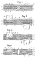
- numeral 1 indicates a multilayer laminate or panel, preferably having a very low coefficient of thermal expansion, which is realized on a first step of the method according to the invention.
- areas 5 and 5A are created on one face of a flat metal layer or element 3, by silk-screen printing or other suitable system, on which areas an insulating or conductive thin layer 6 is in this way applied,capable of de termining, when the cutting edges of a milling cutter 7 or 7A come into contact therewith,a signal which causes the cutter to lift immediately after the removal of the same layer 6, that is, after it has uncovered but not indented the metal of layer 3.
- the layer 6 may be realized in the form of a more or less thin film, usually capable of being easily stripped and made, for example, but not exclusively, of polyimide material being filled or not with extremely fine metal powder; or else, the layer may be constituted by a real electricity conductive metal paste being alloyed with resins being for example but not exclusively, epoxy type resins; in any case, the silk-screen printing process (or other) for the application of the layer 6 may be followed by a phase for the hot-polymerization of the material or of the carrier making part of said layer, in order to achieve a correct anchorage thereof.
- the multilayer laminate 1, for the applications falling within the objects of the invention, is usually made u p , after the application step of layer 6 on the areas 5 and 5A, of two outer copper layers 9, of at least two but preferably three layers of insulating material 11 and of at least one, but preferably two metal layers 3.
- the metal layers 3 are usually continuous throughout the multilayer but, according to the circumstances, may exhibit suitable holes 8 or interruptions or be limited to given zones.
- the layers 11 are usually realized in epoxy resin reinforced with glass fiber cloth, or in polyimide resins reinforced with said cloth; moreover, the interposed metal layers 3 are of "INVAR" alloy or, as shown in the drawing, of a layer of INVAR, together with two upper and lower thin layers of copper.
- the layers 3 cooperate with the material of the layers 11 to give rise to the maximum dimension stability of the multilayer upon the temperature changes. Ln the formation of a multilayer, like that indicated by 1 (with or without the areas 5 and 5a covered with a layer 6), relatively very high temperatures occur which the material of the layer 6 must be able to withstand without having its characteristics changed.
- an electrical signal can be made to correspond, able to automatically drive the immediate removal of the cutter from the multilayer, substantially at the very moment it has finished cutting out a seat 13 whose bottom wall 15 makes part of the upper surface of one of the metal layers 3, as it is shown in Figs.3 and 4.
- a hole 8 relatively larger than the area 5A and the corresponding seat 13A realized by the cutter 7A, must be provided on the layer 3 located in a upper position, in order to avoid undesirable contacts.
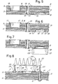
- a subsequent step of the method consists in carrying out a photo-engraving of the outer surface (s) of the multilayer 1 or a selective electro-deposition of metals with a subsequent engraving of the copper, thereby obtaining areas, usually in the form of circular rings like that indicated by 17 and 19 (Fig.6), on which the components CE can be welded or made to rest so that their heat can be dissipated, for example in the disposition of Fig.7, through the metal layers 3 located inside the multilayer.
- a metal paste having a good thermal conductivity can be made to adhere on the base of the component. This paste may also be inserted and distributed on the walls of the metallized cavities thereby further improving the heat transmission.
- the component CE results to be cooled only by the transit of the heat from its base and from the side walls of its lower cylindrical portion to the metal layer 3 with which it is in contact inside the cavity 13, this heat moving along said layer as far as the outside and also being able to dissipate through the other layers of the multilayer.
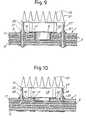
- the method offers the possibility of transferring said amount of heat to an outer dissipator member, like those indicated by 21 in Figs.8 and 9.
- the dissipator member 21, provided with fins 23 to facilitate the air cooling is equipped with at least two metal rods 25 and 27 solid therewith, the one indicated by 25 being inserted and welded in a metallized cavity 29 similar to the cavity 13 and likewise formed, while the rod 27 is inserted and welded in a metallized through-hole 31; both the cavity 29 and the hole 31 being connected, for heat transfer purposes, with the inner layer 3 which receives heat from the component CE.
- the cavity like that indicated by 29 and the holes like that indicated by 31 are suitably located around the component or around groups of components.
- the dissipator member 21 results connected with the inner layer 3 - which receives heat - through at least two rods 25' and 27' both welded inside the metallized through-holes 31', this solution being preferable as the layer 3 is located further in depth, that is, more spaced than in the case shown in Fig.8, in respect to the face of the multilayer on which the component is applied.
- Fig.8 shows an example of mixed (so to speak) connection of the element 21 with the layer 3, that is a connection performed in two different ways
- the rods 25 and 27 are both welded inside cavities 29.
- the layer 3 is usually a layer having the function to "ground” connect the individual components, which are then connected - according to the circuit diagram, by means of weldings 35 - on the portions 19 of the circuit which is printed, that is,photo-engraved on the multilayer after the described metallization step.
- the dissipator members 21 may be also cooled through forced ventilation; moreover, they may be variously shaped as shown in the examples of Fig.11 wherein 21C indicates a plan view of an element being rectangular on top, while 21Q indicates a similar view of a square shaped element made up by the union of four straight elements and which has four rods 23 to receive the heat from the layer 3 being in contact with the component base.
- the method provides also for the utilization of external heat dissipators of tubular (or similar) type, internally cooled by water or other cooling fluid.
- a multilayer 1 with a cavity 13 for a parallelepiped component CE, drawn with dotted lines, results cooled by the cooling liquid circulating in the tubing 39.
- the tubing 39 is supported by and receives the heat from blocks 41 which are provided with lower shanks 43 inserted into metallized through--holes 31 of the multilayer, said shanks receiving the heat from the metal layer 3 on which the component CE rests.
- the heat dissipator, made up of the two right-angle branches of the tubing 39 is substantially similar to that, made up of a U-shaped tubing 45 . borne by blocks 51, shown in plan view on the right in Fig.11.
- the heat dissipation system which results from the invention method is particularly advantageous when multilayers having high dimensional stability like those hereinbefore described are used, in case of possible overheating of the components during their "switch-on/ /switch-off" operation since, in this case, the components thermally expand in a different way from the base support thereof, that is from the multilayer.
- a breaking of the so-called “leadless” (that is, without an intermediate lead) weldings of the components may often occur owing to the above said differences in thermal expansion; a good heat dissipation represents, in this case, a radical solution of the problem.
- the method of the invention can be obviously applied also to multilayers laminates less valuable, so to speak, than those having high dimensional stability as mentioned in this description, that is, multilayers with at least one metal layer disposed inside the insulating layers, all without particular characteristics of non-deformability.
Abstract
Description
- The invention relates to a method to ensure the cooling of electronic components fixed on a multilayer for printed circuits, the multilayer comprising at least a metal layer interposed between insulating layers and, on the outside faces, a copper layer for said circuits; the invention relates also to a multilayer realized according to said method.
- According to the invention, the method comprises the steps of:
- - applying, before the matching of the layers of the multilayer, onto at least one of the faces of the metal layer or of one of the metal layers, a special thin layer or film of insulating or conductive material;
- - creating, through a milling operation, seats or cavities for the insertion of the base portion of the electronic component and possible other seats for the insertion of heat-dissipating rods, the bottom of said seats being made up of said interposed metal layer, for the removal of said special thin layer by means of the milling cutter;
- - forming through-holes in the vicinity of said seats for the insertion of the component base and at close distance from the body outside walls of the component which is to be fixed in each seat;
- - covering, by means of a metallization layer, all the uncovered surfaces of the multilayer, including those of said seats and those inside said through-holes, thereby achieving the electrical and heat transmission connection of all the surfaces covered by the metallization layer;
- - carrying out - through a photoengraving operation, or in another way, on the face or faces of the multilayer on the side wherein said seats are formed - some areas outlining the same seats for the fixing of the component by welding, as well as other areas for connecting, by welding, the component with the printed circuit, and also metal strips making up the leads of said circuit.
- The thin layer or film applied upon the first step is ca= pable of determining an electrical signal which causes the milling cutter to move away - immediately after the removal of the same thin layer, but, in practice, without having indented the metal layer of the multilayer - from the seat it has formed; and the cooling of the component is achievedby heat conduction along said metal layer or by dissipator means located outside the multilayer and in thermal conductivity connection with said metal layer interposed inside the multilayer.
- The invention will be better understood by following the description and the attached drawing which shows a practical non limitative exemplification of the invention itself. In the drawing:
- Fig.1 shows a section view of a laminated multilayer realized according to the method of the invention;
- Figs.2, 3, 4, 5 and 6 are section views illustrating successive phases of said method for the realization of metallized seats and holes for the purposes of the invention;
- Figs.7, 8, 9 and 10 show section views of examples of multilayers with electronic components whose heat dissipation is achieved according to the method of the invention; and
- Figs.11 and 12 show in respective plan and perspective views, examples of members for the heat dissipation of electronic components through air cooling or a cooling fluid.
- According to the attached drawing,
numeral 1 indicates a multilayer laminate or panel, preferably having a very low coefficient of thermal expansion, which is realized on a first step of the method according to the invention. Upon this step,areas 5 and 5A are created on one face of a flat metal layer orelement 3, by silk-screen printing or other suitable system, on which areas an insulating or conductivethin layer 6 is in this way applied,capable of de termining, when the cutting edges of amilling cutter same layer 6, that is, after it has uncovered but not indented the metal oflayer 3. Thelayer 6 may be realized in the form of a more or less thin film, usually capable of being easily stripped and made, for example, but not exclusively, of polyimide material being filled or not with extremely fine metal powder; or else, the layer may be constituted by a real electricity conductive metal paste being alloyed with resins being for example but not exclusively, epoxy type resins; in any case, the silk-screen printing process (or other) for the application of thelayer 6 may be followed by a phase for the hot-polymerization of the material or of the carrier making part of said layer, in order to achieve a correct anchorage thereof. - The
multilayer laminate 1, for the applications falling within the objects of the invention, is usually made up, after the application step oflayer 6 on theareas 5 and 5A, of twoouter copper layers 9, of at least two but preferably three layers ofinsulating material 11 and of at least one, but preferably twometal layers 3. Themetal layers 3 are usually continuous throughout the multilayer but, according to the circumstances, may exhibitsuitable holes 8 or interruptions or be limited to given zones. To obtain a very low coefficient of thermal expansion of themultilayer 1, thelayers 11 are usually realized in epoxy resin reinforced with glass fiber cloth, or in polyimide resins reinforced with said cloth; moreover, the interposedmetal layers 3 are of "INVAR" alloy or, as shown in the drawing, of a layer of INVAR, together with two upper and lower thin layers of copper. Thelayers 3 cooperate with the material of thelayers 11 to give rise to the maximum dimension stability of the multilayer upon the temperature changes. Ln the formation of a multilayer, like that indicated by 1 (with or without the areas 5 and 5a covered with a layer 6), relatively very high temperatures occur which the material of thelayer 6 must be able to withstand without having its characteristics changed. - In the successive steps - which are the ones for use - seats or
dead holes 13 are formed in themultilayer 1 for the fastening of electronic components CE thereon, by means of milling cutters like those indicated by 7 and 7A. The milling operation will be performed by utilizing suitable jigs able to make the drilling coincide with thearea 5 or 5A positions. When the cutting edges of the cutters, like those indicated by 7 and 7A, encounter the layer 6 - which differs from thelayer 11 previously crossed by the cutter - either a sudden change of the cutter rotation speed, or-in case thelayer 6 is formed by a conductive paste , being in contact with the layer 3 - an electrical contact between the cutter and thelayer 6 takes place. In one case or the other, at said sudden speed change or at said electrical contact, an electrical signal can be made to correspond, able to automatically drive the immediate removal of the cutter from the multilayer, substantially at the very moment it has finished cutting out aseat 13 whosebottom wall 15 makes part of the upper surface of one of themetal layers 3, as it is shown in Figs.3 and 4. Moreover, as shown in Figs.1, 2, 3 and 4, upon the formation of themultilayer 1 when thearea 5A finds itself on themetal layer 3 located in a lower position (in the drawing), ahole 8, relatively larger than thearea 5A and thecorresponding seat 13A realized by thecutter 7A, must be provided on thelayer 3 located in a upper position, in order to avoid undesirable contacts. - Further steps for achieving the objects of the invention, that is, for achieving an extremely good dissipation of the heat due to the working of the electronic components CE mounted on the multilayer, are the formation at a suitable position, of one or more through-holes like that indicated by 31, and subsequently, the metallization of all the uncovered surfaces of the multilayer being in the condition shown in Fig.4. By this metallization- which gives rise to a layer 18 - the
cavities 13 obtained through the above described milling operation, have - as shown in Fig.5 - their side surface and their bottom completely metallized, and the outer areas result electrically and thermally connected with the inner metal element orlayer 3. Also the inner walls of the throughholes 31 result metallized. - A subsequent step of the method consists in carrying out a photo-engraving of the outer surface (s) of the
multilayer 1 or a selective electro-deposition of metals with a subsequent engraving of the copper, thereby obtaining areas, usually in the form of circular rings like that indicated by 17 and 19 (Fig.6), on which the components CE can be welded or made to rest so that their heat can be dissipated, for example in the disposition of Fig.7, through themetal layers 3 located inside the multilayer. In order to better help the heat transfer, a metal paste having a good thermal conductivity, can be made to adhere on the base of the component. This paste may also be inserted and distributed on the walls of the metallized cavities thereby further improving the heat transmission. - In the condition shown in Fig.7, the component CE results to be cooled only by the transit of the heat from its base and from the side walls of its lower cylindrical portion to the
metal layer 3 with which it is in contact inside thecavity 13, this heat moving along said layer as far as the outside and also being able to dissipate through the other layers of the multilayer. However, and especially for components whose operating functions give rise to a larger amount of heat to be cooled off, the method offers the possibility of transferring said amount of heat to an outer dissipator member, like those indicated by 21 in Figs.8 and 9. In the example of Fig.8, thedissipator member 21, provided withfins 23 to facilitate the air cooling, is equipped with at least twometal rods metallized cavity 29 similar to thecavity 13 and likewise formed, while therod 27 is inserted and welded in a metallized through-hole 31; both thecavity 29 and thehole 31 being connected, for heat transfer purposes, with theinner layer 3 which receives heat from the component CE. The cavity like that indicated by 29 and the holes like that indicated by 31 are suitably located around the component or around groups of components. In the example of Fig.9, thedissipator member 21 results connected with the inner layer 3 - which receives heat - through at least two rods 25' and 27' both welded inside the metallized through-holes 31', this solution being preferable as thelayer 3 is located further in depth, that is, more spaced than in the case shown in Fig.8, in respect to the face of the multilayer on which the component is applied. Whereas Fig.8 shows an example of mixed (so to speak) connection of theelement 21 with thelayer 3, that is a connection performed in two different ways, in the example of Fig.10, therods cavities 29. - It should be noted that the
layer 3 is usually a layer having the function to "ground" connect the individual components, which are then connected - according to the circuit diagram, by means of weldings 35 - on theportions 19 of the circuit which is printed, that is,photo-engraved on the multilayer after the described metallization step. Thedissipator members 21 may be also cooled through forced ventilation; moreover, they may be variously shaped as shown in the examples of Fig.11 wherein 21C indicates a plan view of an element being rectangular on top, while 21Q indicates a similar view of a square shaped element made up by the union of four straight elements and which has fourrods 23 to receive the heat from thelayer 3 being in contact with the component base. - The method provides also for the utilization of external heat dissipators of tubular (or similar) type, internally cooled by water or other cooling fluid. In Fig.12, a
multilayer 1, with acavity 13 for a parallelepiped component CE, drawn with dotted lines, results cooled by the cooling liquid circulating in thetubing 39. Thetubing 39 is supported by and receives the heat fromblocks 41 which are provided withlower shanks 43 inserted into metallized through--holes 31 of the multilayer, said shanks receiving the heat from themetal layer 3 on which the component CE rests. The heat dissipator, made up of the two right-angle branches of thetubing 39, is substantially similar to that, made up of aU-shaped tubing 45 . borne byblocks 51, shown in plan view on the right in Fig.11. - The heat dissipation system which results from the invention method is particularly advantageous when multilayers having high dimensional stability like those hereinbefore described are used, in case of possible overheating of the components during their "switch-on/ /switch-off" operation since, in this case, the components thermally expand in a different way from the base support thereof, that is from the multilayer. Upon the "switch-on/ /switch-off" operation, a breaking of the so-called "leadless" (that is, without an intermediate lead) weldings of the components may often occur owing to the above said differences in thermal expansion; a good heat dissipation represents, in this case, a radical solution of the problem.
- The method of the invention can be obviously applied also to multilayers laminates less valuable, so to speak, than those having high dimensional stability as mentioned in this description, that is, multilayers with at least one metal layer disposed inside the insulating layers, all without particular characteristics of non-deformability. However, in case of multilayers of the type taken into consideration, the method is capa= ble of advantageously integrating their characteristics by broadening the possibilities of use thereof.
- It is understood that the drawing shows an exemplification given only as a practical demonstration of the invention, as this may vary in the forms and dispositions without nevertheless departing from the scope of the idea on which the same invention is based.
Claims (15)
Applications Claiming Priority (2)
| Application Number | Priority Date | Filing Date | Title |
|---|---|---|---|
| IT943885 | 1985-06-17 | ||
| IT09438/85A IT1201315B (en) | 1985-06-17 | 1985-06-17 | METHOD TO ENSURE THE COOLING OF ELECTRONIC COMPONENTS FIXED ON A MULTILAYER FOR MOLDED AND MULTI-LAYER CIRCUITS REALIZED ACCORDING TO THAT METHOD |
Publications (2)
| Publication Number | Publication Date |
|---|---|
| EP0207012A2 true EP0207012A2 (en) | 1986-12-30 |
| EP0207012A3 EP0207012A3 (en) | 1989-03-15 |
Family
ID=11130144
Family Applications (1)
| Application Number | Title | Priority Date | Filing Date |
|---|---|---|---|
| EP86830164A Ceased EP0207012A3 (en) | 1985-06-17 | 1986-06-11 | Method to ensure the cooling of electronic components fixed on a multilayer for printed circuits and multilayer realized according to said method |
Country Status (6)
| Country | Link |
|---|---|
| US (1) | US4755417A (en) |
| EP (1) | EP0207012A3 (en) |
| JP (1) | JPS61292997A (en) |
| KR (1) | KR900007759B1 (en) |
| CA (1) | CA1263196A (en) |
| IT (1) | IT1201315B (en) |
Cited By (8)
| Publication number | Priority date | Publication date | Assignee | Title |
|---|---|---|---|---|
| DE4012100A1 (en) * | 1990-04-14 | 1991-10-17 | Standard Elektrik Lorenz Ag | Circuit board with cooling unit - has board mounted on plate, with cooler channels coated with metal layer |
| EP0458293A1 (en) * | 1990-05-25 | 1991-11-27 | Sony Corporation | Multilayer wiring board and method for manufacturing the same |
| WO1995011580A1 (en) * | 1993-10-21 | 1995-04-27 | Robert Bosch Gmbh | Circuit-board device |
| EP0989794A2 (en) * | 1998-09-22 | 2000-03-29 | Lucent Technologies Inc. | Surface mount thermal connections |
| WO2004068920A1 (en) * | 2003-01-29 | 2004-08-12 | Koninklijke Philips Electronics N.V. | Heat dissipating arrangement for an electronic appliance |
| GB2415297A (en) * | 2004-06-15 | 2005-12-21 | Radstone Technology Plc | Circuit card with thermally conductive bar |
| WO2011160879A1 (en) * | 2010-06-25 | 2011-12-29 | Zf Friedrichshafen Ag | Electronic control assembly |
| WO2020074201A1 (en) * | 2018-10-10 | 2020-04-16 | Vitesco Technologies Germany Gmbh | Circuit board |
Families Citing this family (9)
| Publication number | Priority date | Publication date | Assignee | Title |
|---|---|---|---|---|
| US4993148A (en) * | 1987-05-19 | 1991-02-19 | Mitsubishi Denki Kabushiki Kaisha | Method of manufacturing a circuit board |
| US4987100A (en) * | 1988-05-26 | 1991-01-22 | International Business Machines Corporation | Flexible carrier for an electronic device |
| US4937707A (en) * | 1988-05-26 | 1990-06-26 | International Business Machines Corporation | Flexible carrier for an electronic device |
| US5248853A (en) * | 1991-11-14 | 1993-09-28 | Nippondenso Co., Ltd. | Semiconductor element-mounting printed board |
| JPH06181390A (en) * | 1992-12-09 | 1994-06-28 | Nec Corp | Multilayer printed-wiring board |
| US6444921B1 (en) | 2000-02-03 | 2002-09-03 | Fujitsu Limited | Reduced stress and zero stress interposers for integrated-circuit chips, multichip substrates, and the like |
| KR20180016799A (en) * | 2016-08-08 | 2018-02-20 | 삼성전자주식회사 | Printed circuit board assembly |
| US11224117B1 (en) * | 2018-07-05 | 2022-01-11 | Flex Ltd. | Heat transfer in the printed circuit board of an SMPS by an integrated heat exchanger |
| CN112518103B (en) * | 2020-12-07 | 2022-10-18 | 中国化学工程第六建设有限公司 | Welding and mounting method for composite board storage tank |
Citations (3)
| Publication number | Priority date | Publication date | Assignee | Title |
|---|---|---|---|---|
| GB2124035A (en) * | 1982-07-15 | 1984-02-08 | Standard Telephones Cables Ltd | Printed circuit boards |
| GB2137422A (en) * | 1983-03-30 | 1984-10-03 | Ferranti Plc | Printed circuit board |
| EP0129966A1 (en) * | 1983-04-22 | 1985-01-02 | Cray Research, Inc. | High cooling efficiency circuit module |
Family Cites Families (1)
| Publication number | Priority date | Publication date | Assignee | Title |
|---|---|---|---|---|
| DE3045433A1 (en) * | 1980-12-02 | 1982-07-01 | Siemens AG, 1000 Berlin und 8000 München | MULTI-LAYER CIRCUIT BOARD AND METHOD FOR DETERMINING THE CURRENT POSITION OF INTERNAL CONNECTION AREAS |
-
1985
- 1985-06-17 IT IT09438/85A patent/IT1201315B/en active
-
1986
- 1986-06-04 US US06/870,522 patent/US4755417A/en not_active Expired - Fee Related
- 1986-06-09 CA CA000511103A patent/CA1263196A/en not_active Expired
- 1986-06-11 EP EP86830164A patent/EP0207012A3/en not_active Ceased
- 1986-06-17 KR KR1019860004791A patent/KR900007759B1/en not_active IP Right Cessation
- 1986-06-17 JP JP61139415A patent/JPS61292997A/en active Pending
Patent Citations (3)
| Publication number | Priority date | Publication date | Assignee | Title |
|---|---|---|---|---|
| GB2124035A (en) * | 1982-07-15 | 1984-02-08 | Standard Telephones Cables Ltd | Printed circuit boards |
| GB2137422A (en) * | 1983-03-30 | 1984-10-03 | Ferranti Plc | Printed circuit board |
| EP0129966A1 (en) * | 1983-04-22 | 1985-01-02 | Cray Research, Inc. | High cooling efficiency circuit module |
Non-Patent Citations (1)
| Title |
|---|
| ELECTRONIC DESIGN, vol. 33, no. 1, 10th January 1985, pages 232-242,244,246,248,250, Hasbrouck Heights, New Jersey, US; M.BEEDIE: "Surface-mounted packaging" * |
Cited By (13)
| Publication number | Priority date | Publication date | Assignee | Title |
|---|---|---|---|---|
| DE4012100A1 (en) * | 1990-04-14 | 1991-10-17 | Standard Elektrik Lorenz Ag | Circuit board with cooling unit - has board mounted on plate, with cooler channels coated with metal layer |
| EP0458293A1 (en) * | 1990-05-25 | 1991-11-27 | Sony Corporation | Multilayer wiring board and method for manufacturing the same |
| US5347712A (en) * | 1990-05-25 | 1994-09-20 | Sony Corporation | Method for manufacturing a multilayer wiring board |
| WO1995011580A1 (en) * | 1993-10-21 | 1995-04-27 | Robert Bosch Gmbh | Circuit-board device |
| EP0989794A2 (en) * | 1998-09-22 | 2000-03-29 | Lucent Technologies Inc. | Surface mount thermal connections |
| EP0989794A3 (en) * | 1998-09-22 | 2000-11-15 | Lucent Technologies Inc. | Surface mount thermal connections |
| US6175500B1 (en) | 1998-09-22 | 2001-01-16 | Lucent Technologies Inc. | Surface mount thermal connections |
| WO2004068920A1 (en) * | 2003-01-29 | 2004-08-12 | Koninklijke Philips Electronics N.V. | Heat dissipating arrangement for an electronic appliance |
| GB2415297A (en) * | 2004-06-15 | 2005-12-21 | Radstone Technology Plc | Circuit card with thermally conductive bar |
| WO2011160879A1 (en) * | 2010-06-25 | 2011-12-29 | Zf Friedrichshafen Ag | Electronic control assembly |
| WO2020074201A1 (en) * | 2018-10-10 | 2020-04-16 | Vitesco Technologies Germany Gmbh | Circuit board |
| KR20210068560A (en) * | 2018-10-10 | 2021-06-09 | 비테스코 테크놀로지스 저머니 게엠베하 | circuit board |
| US11224123B2 (en) | 2018-10-10 | 2022-01-11 | Vitesco Technologies Germany Gmbh | Circuit board |
Also Published As
| Publication number | Publication date |
|---|---|
| CA1263196A (en) | 1989-11-21 |
| US4755417A (en) | 1988-07-05 |
| KR900007759B1 (en) | 1990-10-19 |
| IT1201315B (en) | 1989-01-27 |
| IT8509438A0 (en) | 1985-06-17 |
| JPS61292997A (en) | 1986-12-23 |
| EP0207012A3 (en) | 1989-03-15 |
| KR870000851A (en) | 1987-02-20 |
Similar Documents
| Publication | Publication Date | Title |
|---|---|---|
| EP0207012A2 (en) | Method to ensure the cooling of electronic components fixed on a multilayer for printed circuits and multilayer realized according to said method | |
| US6215681B1 (en) | Bus bar heat sink | |
| US5943216A (en) | Apparatus for providing a two-sided, cavity, inverted-mounted component circuit board | |
| US20040007376A1 (en) | Integrated thermal vias | |
| US3359461A (en) | Modular circuit package | |
| CN107896421B (en) | PCB capable of fast radiating | |
| US5641944A (en) | Power substrate with improved thermal characteristics | |
| JP2004179309A (en) | Heat dissipating structure for printed circuit board and method for manufacturing the same | |
| US6200407B1 (en) | Method of making a multilayer circuit board having a window exposing an enhanced conductive layer for use as an insulated mounting area | |
| JPH07135376A (en) | Composite printed-circuit board and its manufacture | |
| US5565705A (en) | Electronic module for removing heat from a semiconductor die | |
| JP2004072106A (en) | Adjustable pedestal thermal interface | |
| US3646399A (en) | Printed circuit board construction | |
| JP2020515035A (en) | Method for integration of bus bars forming power chip and heat sink | |
| GB2162694A (en) | Printed circuits | |
| US6625026B1 (en) | Heat-activated self-aligning heat sink | |
| EP1528847B1 (en) | Heat dissipating insert, circuit comprising said insert and production method | |
| WO1999011106A1 (en) | A chip supporting element and use thereof | |
| JP2000261152A (en) | Printed wiring board assembly | |
| JPH065994A (en) | Multilayer printed wiring board | |
| JP2004281804A (en) | Circuit board | |
| CN210298190U (en) | PCB structure easy to radiate heat | |
| JP2524733Y2 (en) | Semiconductor device | |
| JP3244003B2 (en) | Circuit board | |
| JPH06125155A (en) | Metal-base circuit board |
Legal Events
| Date | Code | Title | Description |
|---|---|---|---|
| PUAI | Public reference made under article 153(3) epc to a published international application that has entered the european phase |
Free format text: ORIGINAL CODE: 0009012 |
|
| AK | Designated contracting states |
Kind code of ref document: A2 Designated state(s): AT BE CH DE FR GB LI LU NL SE |
|
| PUAL | Search report despatched |
Free format text: ORIGINAL CODE: 0009013 |
|
| AK | Designated contracting states |
Kind code of ref document: A3 Designated state(s): AT BE CH DE FR GB LI LU NL SE |
|
| 17P | Request for examination filed |
Effective date: 19890415 |
|
| 17Q | First examination report despatched |
Effective date: 19900718 |
|
| STAA | Information on the status of an ep patent application or granted ep patent |
Free format text: STATUS: THE APPLICATION HAS BEEN REFUSED |
|
| 18R | Application refused |
Effective date: 19920320 |
|
| RIN1 | Information on inventor provided before grant (corrected) |
Inventor name: DETOMA BIGLIA, RENZO |