EP0211674A2 - Clock signal selection and security arrangements - Google Patents
Clock signal selection and security arrangements Download PDFInfo
- Publication number
- EP0211674A2 EP0211674A2 EP86306167A EP86306167A EP0211674A2 EP 0211674 A2 EP0211674 A2 EP 0211674A2 EP 86306167 A EP86306167 A EP 86306167A EP 86306167 A EP86306167 A EP 86306167A EP 0211674 A2 EP0211674 A2 EP 0211674A2
- Authority
- EP
- European Patent Office
- Prior art keywords
- clock
- signal
- input
- clock signal
- output
- Prior art date
- Legal status (The legal status is an assumption and is not a legal conclusion. Google has not performed a legal analysis and makes no representation as to the accuracy of the status listed.)
- Withdrawn
Links
Images


Classifications
-
- H—ELECTRICITY
- H04—ELECTRIC COMMUNICATION TECHNIQUE
- H04L—TRANSMISSION OF DIGITAL INFORMATION, e.g. TELEGRAPHIC COMMUNICATION
- H04L7/00—Arrangements for synchronising receiver with transmitter
- H04L7/0079—Receiver details
- H04L7/0083—Receiver details taking measures against momentary loss of synchronisation, e.g. inhibiting the synchronisation, using idle words or using redundant clocks
Definitions
- the present invention relates to clock signal selection and security arrangements and more particularly but not exclusively to such arrangements for use in a time-division-multiplexed pulse-code- modulated digital signal switching system.
- a clock signal security arrangement comprising inputs for at least three corresponding clock signals, averaging means arranged to provide a comparison clock signal derived from all of the clock input signals, and comparison means arranged to compare each input clock signal with said comparison clock signal, said comparison means providing an output signal in dependance upon the validity of each of said clock input signals.
- said arrangement also comprises delay means arranged to provide a delayed clock signal derived from said comparison clock signal, and said comparison means is enabled when both said delayed clock signal and said comparison clock signal are at the same value the delay being selected such that comparison of the input clock signals with the comparison clock signal occurs substantially mid-way through a pulse period of the comparison clock signal.
- the comparison clock signal is selected for output as a controlling clock signal.
- one of the input clock signals is selected for output as a controlling clock signal in dependance upon the output of the comparison means.
- an input clock signal present on a first input is selected for output as the controlling clock signal unless said clock signal is determined as faulty by the comparison means. If the clock signal present on said first input is determined as faulty by satd comparison means the clock signal on a second input is selected for output as the controlling clock signal.
- the selection of the controlling signal may be by a circuit comprising a first logic gate which receives the first clock input signal, and a second logic gate which receives the second clock input signal, said first logic gate outputting either the first clock input signal or an enable signal to said second logic gate in dependance upon the output of the comparison means, said second logic gate passing either the first clock signal or the second clock signal.
- the comparison means may be arranged to output a signal to control means indicating the presence of a fault in one of the input clock signals to provide an interrupt signal to such control means.
- a data signal indicating which of the input clock signals is faulty may be output in parallel with said interrupt signal.
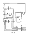
- the system accepts three levels of each of two clocks from a telecommunications exchange clock generation system (not shown).
- the first clock at 2048 kilohertz is received on inputs 1,2 and 3 whilst the second clock, an eight kilohertz time-division-multiplex - (TDM) frame synchronisation signal is received on inputs 41,42 and 43.
- TDM time-division-multiplex -
- An adder circuit 10 performs a two out of three majority decision on the three clock levels which majority decision is distributed by a connection 11 to various fault detection elements of the circuit.
- the majority decision clock is not used as the master clock signal to be supplied since if a fault is present an uneven mark/space ratio may be generated if skew due to differential input delays is present in one or both of the two majority clocks.
- the majority decision clock is used as a comparison signal in the fault detection circuitry which comprises three comparison gates 17,18,19 whence the clock signals on connections 7,8 and 9 are respectively fed by way of respective bistable elements in a circuit 12 via respective connections on leads 14,15,16.
- the majority clock on lead 11 is fed by way of a respective bistable element in the circuit 12 on a connection 13 to the other inputs of each of the comparison gates 17,18,19.
- the signal from the first clock comparison gate 17 is inverted by a NOR gate 28' to provide an enable signal via connection 27 to enable a gate 25 which is also enabled by the signal on the connection 21 from the gate 18 if the second clock signal from the input 2 is satisfactory.
- the clock signal on connection 8 is enabled through the gate 25 and the gate 24 to provide the master clock on the lead 26.
- the output signal from the gate 28' via the connection 27 disables the gate 25 to prevent the passage of the clock signal received on the input 2 to the output lead 26. It may be seen therefore that if the clock on the input 1 is satisfactory it acts as the master clock regardless of the condition of the clock on the input 2. However, if the clock on the input 1 is determined as faulty, the clock on the input 2 acts as the master clock.
- the clock provided on the input 3 serves only as an arbiter for the majority decision logic and is not selected for output.
- any of the three clocks on the inputs 1,2 or 3 is determined as faulty, it is necessary for an alarm condition to be generated. This is achieved by combining the three clock condition signals from the gates 17, 18 and 19 in a gate 28 which outputs a signal on connection 29 if any fault output is present. This signal passes by way of a bistable circuit in a logic circuit 30 to a NAND gate 31 which, if either input changes, forwards an interrupt signal on a lead 32 to the exchange control system (not shown) indicating a clock failure.
- an indication of the presence of a clock fault is output through a multiplexer contained in a circuit 33 together with an indication of which clock is at fault output through three other multiplexers either in the circuit 33 or in a circuit 34 to data leads 35-38.
- the function of the other multiplexer inputs will become apparent from the description which follows relating to the second group of clocks.
- clocking of the bistable circuit 12 to effect comparison of the clocks is derived from the average clock on connection 11 from the adder 10 by way of a delay circuit 39 and a gate 40.
- the delay is selected to be approximately 120 nano seconds incorporated in a commercially available selectable delay circuit. This ensures that comparison of the clock signals occurs after the input clock transitions.
- the three levels of frame synchronisation clock are received on inputs 41,42 and 43 and pass via receivers 44,45 and 46 and connections 47,48 and 49 to the adder circuit 10. In this case the output of the adder circuit 10. a two out of three majority signal is fed directly to output 50 for use as the system frame synchronisation signal.
- This average clock on connection 50 together with the three clock signals received now passes by way of a respective bistable circuit 52 and connection 53 to three comparison gates 57,58,59 which, in the same manner as the gates 17,18,19 determines whether any of the three clock signals are faulty. If one of the clocks is determined as faulty a NOR gate 60 connected to a respective bistable element in the circuit 30 causes the output of an interrupt signal by way of NAND gate 31 and lead 32 in the same manner as the main clock signal.
- a clock fault indication is provided through the first four to one multiplexer circuit in element 33 to the data output 35 with an indication of the faulty clock through respective multiplexers of elements 33 and 34 to data outputs 36,37 and 38.
- bistable circuit 52 is clocked from the two megahertz main clock signal. It will also be noted that the unconnected inputs of the multiplexers of elements 33 and 34 are available for other fault reporting circuits such as pcm speech paths (not shown).
- a reset signal may be applied to lead 61 connected to the bistable elements 12,52 to clear any fault indications occurring on (eg.) intiatisation of a connected system.
Abstract
Description
- The present invention relates to clock signal selection and security arrangements and more particularly but not exclusively to such arrangements for use in a time-division-multiplexed pulse-code- modulated digital signal switching system.
- In our co-pending Patent Application No........ line terminating apparatus for use in a digital switching system (such as the system known in the United Kingdom as System X) is described.
- In such complex switching systems faults in for example time-division multiplex frame synchronisation or other clock functions may cause a communications failure. Accordingly monitoring clock signals in peripheral units and responding rapidly to fault conditions encountered thereon are important functions.
- It is one object of the present invention to provide a clock signal selection and security arrangement capable of meeting the stringent demands of a telecommunications system.
- According to the present invention there is provided a clock signal security arrangement comprising inputs for at least three corresponding clock signals, averaging means arranged to provide a comparison clock signal derived from all of the clock input signals, and comparison means arranged to compare each input clock signal with said comparison clock signal, said comparison means providing an output signal in dependance upon the validity of each of said clock input signals.
- Preferably said arrangement also comprises delay means arranged to provide a delayed clock signal derived from said comparison clock signal, and said comparison means is enabled when both said delayed clock signal and said comparison clock signal are at the same value the delay being selected such that comparison of the input clock signals with the comparison clock signal occurs substantially mid-way through a pulse period of the comparison clock signal.
- In one embodiment of the arrangement the comparison clock signal is selected for output as a controlling clock signal.
- In a preferred embodiment of the arrangement one of the input clock signals is selected for output as a controlling clock signal in dependance upon the output of the comparison means.
- In the preferred embodiment an input clock signal present on a first input is selected for output as the controlling clock signal unless said clock signal is determined as faulty by the comparison means. If the clock signal present on said first input is determined as faulty by satd comparison means the clock signal on a second input is selected for output as the controlling clock signal.
- The selection of the controlling signal may be by a circuit comprising a first logic gate which receives the first clock input signal, and a second logic gate which receives the second clock input signal, said first logic gate outputting either the first clock input signal or an enable signal to said second logic gate in dependance upon the output of the comparison means, said second logic gate passing either the first clock signal or the second clock signal.
- The comparison means may be arranged to output a signal to control means indicating the presence of a fault in one of the input clock signals to provide an interrupt signal to such control means. A data signal indicating which of the input clock signals is faulty may be output in parallel with said interrupt signal.
- Clock signal selection and security arrangements in accordance with the invention will now be described by way of example only with reference to the accompanying drawings which when assembled as shown is a circuit diagram of the arrangement.
- Referring to the drawings the system accepts three levels of each of two clocks from a telecommunications exchange clock generation system (not shown). The first clock at 2048 kilohertz is received on
inputs inputs - Since the two clocks are handled in a slightly different manner the circuit functions will be considered separately. Thus commencing with the
clock inputs differential line receivers respective connections - An
adder circuit 10 performs a two out of three majority decision on the three clock levels which majority decision is distributed by aconnection 11 to various fault detection elements of the circuit. However, the majority decision clock is not used as the master clock signal to be supplied since if a fault is present an uneven mark/space ratio may be generated if skew due to differential input delays is present in one or both of the two majority clocks. The majority decision clock is used as a comparison signal in the fault detection circuitry which comprises three comparison gates 17,18,19 whence the clock signals onconnections circuit 12 via respective connections onleads lead 11 is fed by way of a respective bistable element in thecircuit 12 on aconnection 13 to the other inputs of each of the comparison gates 17,18,19. - Considering the output of the comparator 17 on
connection 20, assuming that the clock at theinput 1 is satisfactory then the clock signal feeds through agate 23 and agate 24 to provide the master clock output signal on alead 25. However, if the first clock is faulty thengate 23 is disabled. - Similarly the signal from the first clock comparison gate 17 is inverted by a NOR gate 28' to provide an enable signal via
connection 27 to enable agate 25 which is also enabled by the signal on theconnection 21 from the gate 18 if the second clock signal from theinput 2 is satisfactory. Thus the clock signal onconnection 8 is enabled through thegate 25 and thegate 24 to provide the master clock on thelead 26. - It will be appreciated that when the clock signal on the
input 1 is satisfactory, the output signal from the gate 28' via theconnection 27 disables thegate 25 to prevent the passage of the clock signal received on theinput 2 to theoutput lead 26. It may be seen therefore that if the clock on theinput 1 is satisfactory it acts as the master clock regardless of the condition of the clock on theinput 2. However, if the clock on theinput 1 is determined as faulty, the clock on theinput 2 acts as the master clock. The clock provided on theinput 3 serves only as an arbiter for the majority decision logic and is not selected for output. - If any of the three clocks on the
inputs gate 28 which outputs a signal onconnection 29 if any fault output is present. This signal passes by way of a bistable circuit in alogic circuit 30 to aNAND gate 31 which, if either input changes, forwards an interrupt signal on alead 32 to the exchange control system (not shown) indicating a clock failure. - Simultaneously an indication of the presence of a clock fault is output through a multiplexer contained in a
circuit 33 together with an indication of which clock is at fault output through three other multiplexers either in thecircuit 33 or in acircuit 34 to data leads 35-38. The function of the other multiplexer inputs will become apparent from the description which follows relating to the second group of clocks. - It will be noted that clocking of the
bistable circuit 12 to effect comparison of the clocks is derived from the average clock onconnection 11 from theadder 10 by way of adelay circuit 39 and agate 40. The delay is selected to be approximately 120 nano seconds incorporated in a commercially available selectable delay circuit. This ensures that comparison of the clock signals occurs after the input clock transitions. - The three levels of frame synchronisation clock are received on
inputs receivers connections adder circuit 10. In this case the output of theadder circuit 10. a two out of three majority signal is fed directly tooutput 50 for use as the system frame synchronisation signal. - This average clock on
connection 50 together with the three clock signals received now passes by way of a respectivebistable circuit 52 andconnection 53 to threecomparison gates NOR gate 60 connected to a respective bistable element in thecircuit 30 causes the output of an interrupt signal by way ofNAND gate 31 and lead 32 in the same manner as the main clock signal. - Similarly a clock fault indication is provided through the first four to one multiplexer circuit in
element 33 to thedata output 35 with an indication of the faulty clock through respective multiplexers ofelements data outputs - ft will be noted that the
bistable circuit 52 is clocked from the two megahertz main clock signal. It will also be noted that the unconnected inputs of the multiplexers ofelements - A reset signal may be applied to lead 61 connected to the
bistable elements - For the avoidance of doubt the following commercially available integrated circuits may be used to construct the circuit shown in the drawings:-
-
Receivers
Claims (2)
- comparison means outputs an interrupt signal to control means said interrupt signal indicating the presence of a fault.
- 9. A clock signal security arrangement according to claim 8 wherein said comparison means also outputs a data signal indicating which of the input signals is detected as having a fault.
Applications Claiming Priority (2)
| Application Number | Priority Date | Filing Date | Title |
|---|---|---|---|
| GB08520035A GB2178926A (en) | 1985-08-09 | 1985-08-09 | Clock signal selection and security arrangements |
| GB8520035 | 1985-08-09 |
Publications (2)
| Publication Number | Publication Date |
|---|---|
| EP0211674A2 true EP0211674A2 (en) | 1987-02-25 |
| EP0211674A3 EP0211674A3 (en) | 1989-01-18 |
Family
ID=10583551
Family Applications (1)
| Application Number | Title | Priority Date | Filing Date |
|---|---|---|---|
| EP86306167A Withdrawn EP0211674A3 (en) | 1985-08-09 | 1986-08-08 | Clock signal selection and security arrangements |
Country Status (5)
| Country | Link |
|---|---|
| EP (1) | EP0211674A3 (en) |
| JP (1) | JPS62168438A (en) |
| FI (1) | FI863224A (en) |
| GB (1) | GB2178926A (en) |
| ZA (1) | ZA865726B (en) |
Cited By (1)
| Publication number | Priority date | Publication date | Assignee | Title |
|---|---|---|---|---|
| WO2000060806A2 (en) * | 1999-04-02 | 2000-10-12 | Storage Technology Corporation | Dropout resistant phase-locked loop |
Citations (2)
| Publication number | Priority date | Publication date | Assignee | Title |
|---|---|---|---|---|
| US3686657A (en) * | 1970-02-27 | 1972-08-22 | Lannionnais Electronique | Device for distributing high-safety time bases |
| US4322580A (en) * | 1980-09-02 | 1982-03-30 | Gte Automatic Electric Labs Inc. | Clock selection circuit |
Family Cites Families (2)
| Publication number | Priority date | Publication date | Assignee | Title |
|---|---|---|---|---|
| IT1051350B (en) * | 1975-12-09 | 1981-04-21 | Cselt Centro Studi Lab Telecom | TRIPLE TIMING SYSTEM FOR DUPLICATED SYSTEMS CONTE NENTI LOGIC CIRCUITS |
| FR2577087B1 (en) * | 1985-02-07 | 1987-03-06 | Thomson Csf Mat Tel | TRIPLICATED CLOCK DELIVERY DEVICE, EACH CLOCK SIGNAL HAVING A SYNCHRONIZATION SIGNAL |
-
1985
- 1985-08-09 GB GB08520035A patent/GB2178926A/en not_active Withdrawn
-
1986
- 1986-07-31 ZA ZA865726A patent/ZA865726B/en unknown
- 1986-08-06 FI FI863224A patent/FI863224A/en not_active IP Right Cessation
- 1986-08-08 EP EP86306167A patent/EP0211674A3/en not_active Withdrawn
- 1986-08-08 JP JP61186695A patent/JPS62168438A/en active Pending
Patent Citations (2)
| Publication number | Priority date | Publication date | Assignee | Title |
|---|---|---|---|---|
| US3686657A (en) * | 1970-02-27 | 1972-08-22 | Lannionnais Electronique | Device for distributing high-safety time bases |
| US4322580A (en) * | 1980-09-02 | 1982-03-30 | Gte Automatic Electric Labs Inc. | Clock selection circuit |
Cited By (3)
| Publication number | Priority date | Publication date | Assignee | Title |
|---|---|---|---|---|
| WO2000060806A2 (en) * | 1999-04-02 | 2000-10-12 | Storage Technology Corporation | Dropout resistant phase-locked loop |
| WO2000060806A3 (en) * | 1999-04-02 | 2001-01-25 | Storage Technology Corp | Dropout resistant phase-locked loop |
| US6775344B1 (en) | 1999-04-02 | 2004-08-10 | Storage Technology Corporation | Dropout resistant phase-locked loop |
Also Published As
| Publication number | Publication date |
|---|---|
| JPS62168438A (en) | 1987-07-24 |
| ZA865726B (en) | 1988-11-30 |
| FI863224A0 (en) | 1986-08-06 |
| EP0211674A3 (en) | 1989-01-18 |
| GB2178926A (en) | 1987-02-18 |
| GB8520035D0 (en) | 1985-09-18 |
| FI863224A (en) | 1987-02-10 |
Similar Documents
| Publication | Publication Date | Title |
|---|---|---|
| US4279034A (en) | Digital communication system fault isolation circuit | |
| US4945540A (en) | Gate circuit for bus signal lines | |
| JP2002503371A (en) | Majority hardware design and majority testing and maintenance | |
| US5357491A (en) | Clock selection control device | |
| KR100217516B1 (en) | Method and device for supervising and testing majority voting | |
| CA1089996A (en) | Safety output control for a data processing system emitting binary signals | |
| EP0211674A2 (en) | Clock signal selection and security arrangements | |
| US4949334A (en) | Protected information transfer system | |
| KR900005727A (en) | Protection against loss or transfer of data due to switchover of replication systems | |
| JP2692338B2 (en) | Communication device failure detection device | |
| JP3686752B2 (en) | Clock dependent selection circuit | |
| AU630993B2 (en) | Module disabling circuit | |
| JP2869284B2 (en) | Signaling signal error protection circuit | |
| JPS6339254A (en) | Fault detecting device for digital exchange | |
| SU966904A1 (en) | Pulse distributor | |
| JP2721457B2 (en) | Signal switching circuit | |
| SU1562898A1 (en) | Multichannel device for information input/output | |
| JP2569892B2 (en) | Switching control monitoring circuit | |
| JPS63240145A (en) | Digital signal transmission system | |
| SU1091168A1 (en) | Device for control of switching backup blocks | |
| JPS5872226A (en) | Clock switching circuit | |
| KR930007474B1 (en) | D-bus address detecting circuit in electronic exchanges | |
| JP2000324201A (en) | Communication device | |
| JP3016280B2 (en) | In-device monitoring method | |
| JPH0556022A (en) | Transmission line switching circuit |
Legal Events
| Date | Code | Title | Description |
|---|---|---|---|
| PUAI | Public reference made under article 153(3) epc to a published international application that has entered the european phase |
Free format text: ORIGINAL CODE: 0009012 |
|
| AK | Designated contracting states |
Kind code of ref document: A2 Designated state(s): BE CH DE FR IT LI NL SE |
|
| PUAL | Search report despatched |
Free format text: ORIGINAL CODE: 0009013 |
|
| AK | Designated contracting states |
Kind code of ref document: A3 Designated state(s): BE CH DE FR IT LI NL SE |
|
| STAA | Information on the status of an ep patent application or granted ep patent |
Free format text: STATUS: THE APPLICATION IS DEEMED TO BE WITHDRAWN |
|
| 18D | Application deemed to be withdrawn |
Effective date: 19890719 |
|
| RIN1 | Information on inventor provided before grant (corrected) |
Inventor name: MELINN, FRANCIS Inventor name: GREENLAND, ROGER |