EP0212898A2 - Analog-to-digital converter - Google Patents
Analog-to-digital converter Download PDFInfo
- Publication number
- EP0212898A2 EP0212898A2 EP86305966A EP86305966A EP0212898A2 EP 0212898 A2 EP0212898 A2 EP 0212898A2 EP 86305966 A EP86305966 A EP 86305966A EP 86305966 A EP86305966 A EP 86305966A EP 0212898 A2 EP0212898 A2 EP 0212898A2
- Authority
- EP
- European Patent Office
- Prior art keywords
- capacitor
- switching
- switching capacitor
- input
- analog signal
- Prior art date
- Legal status (The legal status is an assumption and is not a legal conclusion. Google has not performed a legal analysis and makes no representation as to the accuracy of the status listed.)
- Granted
Links
Images
Classifications
-
- H—ELECTRICITY
- H03—ELECTRONIC CIRCUITRY
- H03M—CODING; DECODING; CODE CONVERSION IN GENERAL
- H03M1/00—Analogue/digital conversion; Digital/analogue conversion
- H03M1/12—Analogue/digital converters
-
- H—ELECTRICITY
- H03—ELECTRONIC CIRCUITRY
- H03M—CODING; DECODING; CODE CONVERSION IN GENERAL
- H03M1/00—Analogue/digital conversion; Digital/analogue conversion
- H03M1/12—Analogue/digital converters
- H03M1/50—Analogue/digital converters with intermediate conversion to time interval
- H03M1/54—Input signal sampled and held with linear return to datum
Definitions
- This invention relates to analog-to-digital converters.
- V/F voltage to frequency
- V/F converters can be utilised, they are relatively slow in response time and low in accuracy.
- the slow conversion of the V/F converter results from the need for a counting interval that is at least as long as the period for the lowest frequency signal.
- the response time is a fixed value regardless of the frequency of the signal. This means that a microprocessor used in conjunction with the V/F converter will be tied up during this conversion time. This limits the overall response of the pressure transducer.
- accuracy a moderate-precision V/F circuit has an accuracy range of about 0.4% to 0.1%. To obtain a high-precision V/F circuit with an accuracy range of 0.03% to 0.01% requires additional components which result in greater power consumption and higher cost.
- a converter which operates at low power consumption and with high accuracy would be particularly useful for a two-wire 4-20 mA current loop.
- Two-wire analog transmission systems are known. Such systems include a transmitter which is connected to a power supply by two wires which form a current loop.
- the transmitter includes, as at least one of its features, a transducer which senses a condition such as pressure or temperature. This condition is known as a process variable (PV).
- PV process variable
- a power supply is connected to the two wires to close the current loop. It is also known to provide a resistor in the current loop.
- the transmitter amplifies the signal from its transducer and this amplified signal is used to draw a certain current from the power supply which is proportional or otherwise related to the process variable. It is also known to draw from a minimum of 4 mA to a maximum of 20 mA. The current between 4 and 20 mA passes through the resistor to produce a voltage drop across the resistor. This voltage drop can be measured to give a value for the process variable.
- the 4 mA minimum current is required to energise the circuitry of the transmitter. Any excess current above this 4 mA level is taken as a value which can be used to determine the process variable.
- a converter for converting an analog signal to a digital pulse comprising:
- a converter for converting an analog signal into a digital pulse which converter comprises a switching capacitor, an input circuit connectable to the switching capacitor for applying an analog signal to the switching capacitor to charge the capacitor to a charge level which is proportional to the analog signal, an output circuit which is connectable to the switching capacitor and which includes a constant current source for discharging the switching capacitor from the charge level to a selected low level during a discharge period, switching logic means connected to the input and output circuits for connecting the input circuit to the capacitor while the output circuit is disconnected from the capacitor during a charging period which is sufficiently long to charge the capacitor to its charge level, and for disconnecting the input circuit while the output circuit is connected to the capacitor for discharging the capacitor from the charged level to the selected level during a time which is at least greater than the discharging period, and a pulse generating circuit connected to the output circuit for generating a pulse which has a duration equal or proportional to the discharging period, the pulse being usable as a digital pulse signal which is proportional to the
- a further aspect of the invention provides a method of analog to digital conversion which method comprises charging a switching capacitor during a charging period to a charge level which is proportional to an analog signal, discharging the capacitor during a discharging period over a constant current source down from the charged level to a selected low level, and generating a digital pulse having a width which is equal to the discharging period and which can be utilised as digital pulse corresponding to the analog signal.
- a preferred form of converter embodying the present invention and described hereinbelow utilises a voltage to pulse (V/P) principle whEch operates with less than 3 mW of power.
- the pulse duration of an output signal from the converter is proportional to an analog input signal.
- the conversion time and accuracy of the V/P converter, with minimal components for low power dissipation, is an improvement over known V/F converters. Further improvements in accuracy and conversion time are obtained by using input auto-ranging.
- an associated microprocessor will be tied up only for the pulse duration time period.
- the low power consumption is a result of the minimal number of components needed to implement the V/P circuit and the utilisation of low power integrated circuits. Even with this minimal component count, the average tested accuracy of the V/P circuit is +0.03%.
- the preferred voltage-to-pulse converter has low power consumption, high accuracy and is simple in design, rugged in construction and economical to manufacture.
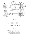
- Figure 1 shows a voltage-to-pulse converter which includes a switching capacitor 10 that is connectable selectively to an input circuit 12 and an output circuit 14.
- a sensor 16 such as a differential strain gauge transducer, has a pair of outputs at 18 and 20 which carry different analog voltages which correspond to a differential in pressure being measured by the sensor 16.
- Each output 18,20 is connected to a respective operational amplifier 22 and 23, which amplifiers are connected together to form a high input impedance differential amplifier.
- the input circuit 12 includes a pair of electronic input switches 24 and 25 which can be closed simultaneously by a signal on a line 26. By applying an appropriate logical signal on the line 26, both the switches 24 and 25 are closed.
- the analog signal on the lines 18 and 20 is thus applied, via the operational amplifiers, to the switching capacitor 10. As long as the switches 24,25 are closed for a long enough charging period, the capacitor 10 will be charged up to a level which is proportional to the differential signal on the lines 18 and 20.
- the output circuit 14 includes a pair of output switches 34 and 35 which can be closed simultaneously by a line 36.
- the line 36 is connected to an output of an inverter 40.
- a line 42 is connected to an input of the inverter 40 and also directly to the line 26. In this way, a high or logical 1 signal applied to the line 42 will cause the switches 24,25 to close while the switches 34,35 are held open. Conversely if a low or logical 0 signal is applied to the line 42, the switches 24,25 are open and the switches 34,35 are closed.
- the output circuit 14 includes a constant current supply or source 44 which, with the switches 34,35 closed, causes the switching capacitor 10 to discharge at a fixed rate. The time it takes the capacitor 10 to discharge from its charged level to a selected discharged or low level is utilised to generate a pulse having a width which is equal to that discharge period.
- the pulse is generated by a comparator 46 which can be in the form of a differential amplifier having a positive (non-inverting) input connected to one side of the capacitor 10 and a negative (inverting) input connected to a terminal B.
- the terminal B receives a trip point voltage which determines the level at which the comparator 46 will output a signal on an output terminal A thereof.
- the discharging time for the capacitor 10 can also be modified by utilising a bias input which is applied to a terminal C of an amplifier 48.
- the terminal C can be used for reference and auto-ranging to compensate for factors which might cause the sensor 16 to drift, such as temperature and other pressure conditions.
- the terminals A, B and C are connected to a microprocessor 50 which is connected to a clock 52. With the aid of the clock 52, the microprocessor 50 outputs signals onto the line 42. In this way, pulse trains similar to those shown in Figures 2 and 3 can be generated. Both Figures 2 and 3 assume a pulse width or spacing of 80 ms. It is always assumed that the width of the pulses is at least as great as the maximum time it takes the capacitor 10 to be fully charged to its charged level, and fully discharged to the selected low level.
- FIG. 2 shows an example where the generated pulse is on for one-half of the pulse train period.
- the capacitor 10 is assumed already to have been charged to its charge level by the differential signal on the lines 18 and 20.
- the microprocessor 50 generates a logical 0 signal on the line 42. This closes the switches 34,35 and opens the switches 24,25.
- the capacitor 10 then immediately begins to discharge via the constant current source 44.
- the comparator 46 outputs a high voltage signal, shown as 5 volts in Figure 2. This continues until 40 ms into the first pulse, whereupon the level at the positive input of the comparator 46 is equal to the trip point voltage applied to the terminal B by the microprocessor 50.
- the output of the comparator 46 drops to 0 as shown in Figure 2.
- the microprocessor 50 may immediately generate a logical I signal on the line 42 to close the switches 24,25 and open the switches 34,35.
- Figure 3 shows the case where there is a lower differential signal on the lines 18 and 20 and thereby a correspondingly shorter pulse width.
- the converter described above thus enables pulses having a variable duty cycle to be generated, the duty cycle being a digital representation of the analog signal.
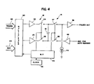
- Converters embodying the invention can be utilised with a 4-20 mA current loop where maximum power dissipation is limited to 48 mW.
- a differential input multiplexer 60 is used with a plurality of inputs 62 from a plurality of transducers, and a plurality of inputs 64 which can be used for auto-ranging.
- the four inputs of the multiplexer 60 can be dedicated for the transducer inputs 62 and four other inputs for the inputs 64.
- the multiplexer 60 sequentially selects one of the eight available inputs at a time for the amplifiers 22 and 23 of the input circuit 12.
- the same reference numerals are utilised to designate same or similar parts as in Figure 1.
- the multiplexer 60 is controlled by the microprocessor 50.
- the switches 24,25 and 34,35 are also controlled by the microprocessor 50, with priming established by the clock 52, to charge and discharge the capacitor 10.
- the comparator 46 generates output pulses while the amplifier 48 processes the reference signal for auto-ranging.
- a constant current supply or source 44 is utilised for discharging the capacitor 10 at constant rate to establish the duty cycle for the output pulses.
Abstract
Description
- This invention relates to analog-to-digital converters.
- Signal conversion of an analog signal to a digital signal for digital processing in low power applications, such as pressure transducers, is normally accomplished by a voltage to frequency (V/F) converter. Commercially available A/D converters are not utilised due to their excessive power consumption. There are not commercially available integrated circuits for analog to digital conversion that are of sufficiently low power, that is less than 12 mW, to run from a 4-20 mA current loop.
- While V/F converters can be utilised, they are relatively slow in response time and low in accuracy. The slow conversion of the V/F converter results from the need for a counting interval that is at least as long as the period for the lowest frequency signal. The response time is a fixed value regardless of the frequency of the signal. This means that a microprocessor used in conjunction with the V/F converter will be tied up during this conversion time. This limits the overall response of the pressure transducer. With regard to accuracy, a moderate-precision V/F circuit has an accuracy range of about 0.4% to 0.1%. To obtain a high-precision V/F circuit with an accuracy range of 0.03% to 0.01% requires additional components which result in greater power consumption and higher cost.
- A converter which operates at low power consumption and with high accuracy would be particularly useful for a two-wire 4-20 mA current loop.
- Two-wire analog transmission systems are known. Such systems include a transmitter which is connected to a power supply by two wires which form a current loop. The transmitter includes, as at least one of its features, a transducer which senses a condition such as pressure or temperature. This condition is known as a process variable (PV).
- A power supply is connected to the two wires to close the current loop. It is also known to provide a resistor in the current loop. The transmitter amplifies the signal from its transducer and this amplified signal is used to draw a certain current from the power supply which is proportional or otherwise related to the process variable. It is also known to draw from a minimum of 4 mA to a maximum of 20 mA. The current between 4 and 20 mA passes through the resistor to produce a voltage drop across the resistor. This voltage drop can be measured to give a value for the process variable.
- It is noted that the 4 mA minimum current is required to energise the circuitry of the transmitter. Any excess current above this 4 mA level is taken as a value which can be used to determine the process variable.
- It is known that such 4-20 mA two-wire systems have an accuracy which is limited to around 0.1% at best. These systems are also essentially unidirectional with the transmitter being essentially uncontrolled and transmitting continuously.
- According to one aspect of the present invention there is provided a converter for converting an analog signal to a digital pulse, the converter comprising:
- a switching capacitor;
- an input circuit connectable to the switching capacitor for applying an analog signal to the switching capacitor to charge the switching capacitor to a charge level which is proportional to the analog signal;
- an output circuit connectable to the switching capacitor and including a constant current source for discharging the switching capacitor from its charge level to a selected low level during a discharging period;
- switching logic means connected to the input and output circuits for connecting the input and output circuits one at a time to the switching capacitor for charging the switching capacitor to its charge level and for discharging the switching capacitor to the selected low level, the switching logic means connecting the switching capacitor to the input circuit for a sufficient time to reach the charge level and connecting the switching capacitor to the output circuit for a time longer than the discharging period; and
- pulse generating means connected to the output circuit for generating a digital pulse having a duration equaling the discharge period.
- According to another aspect of the present invention there is provided a converter for converting an analog signal into a digital pulse, which converter comprises a switching capacitor, an input circuit connectable to the switching capacitor for applying an analog signal to the switching capacitor to charge the capacitor to a charge level which is proportional to the analog signal, an output circuit which is connectable to the switching capacitor and which includes a constant current source for discharging the switching capacitor from the charge level to a selected low level during a discharge period, switching logic means connected to the input and output circuits for connecting the input circuit to the capacitor while the output circuit is disconnected from the capacitor during a charging period which is sufficiently long to charge the capacitor to its charge level, and for disconnecting the input circuit while the output circuit is connected to the capacitor for discharging the capacitor from the charged level to the selected level during a time which is at least greater than the discharging period, and a pulse generating circuit connected to the output circuit for generating a pulse which has a duration equal or proportional to the discharging period, the pulse being usable as a digital pulse signal which is proportional to the analog signal.
- A further aspect of the invention provides a method of analog to digital conversion which method comprises charging a switching capacitor during a charging period to a charge level which is proportional to an analog signal, discharging the capacitor during a discharging period over a constant current source down from the charged level to a selected low level, and generating a digital pulse having a width which is equal to the discharging period and which can be utilised as digital pulse corresponding to the analog signal.
- A preferred form of converter embodying the present invention and described hereinbelow utilises a voltage to pulse (V/P) principle whEch operates with less than 3 mW of power. The pulse duration of an output signal from the converter is proportional to an analog input signal. The conversion time and accuracy of the V/P converter, with minimal components for low power dissipation, is an improvement over known V/F converters. Further improvements in accuracy and conversion time are obtained by using input auto-ranging. By utilising such a V/P technique, an associated microprocessor will be tied up only for the pulse duration time period. The low power consumption is a result of the minimal number of components needed to implement the V/P circuit and the utilisation of low power integrated circuits. Even with this minimal component count, the average tested accuracy of the V/P circuit is +0.03%. The preferred voltage-to-pulse converter has low power consumption, high accuracy and is simple in design, rugged in construction and economical to manufacture.
- The invention will now be further described, by way of illustrative and non-limiting example, with reference to the accompanying drawings, in which:
- Figure 1 is a schematic block diagram of one voltage-to-pulse converter embodying the invention;
- Figure 2 is a graph showing a pulse train which can be generated by the converter;
- Figure 3 is a graph, similar to Figure 2, showing a pulse having a different duty cycle which can be generated by the converter when it receives a different lower analog signal; and
- Figure 4 is a schematic block diagram showing another converter embodying the invention.
- Figure 1 shows a voltage-to-pulse converter which includes a
switching capacitor 10 that is connectable selectively to aninput circuit 12 and anoutput circuit 14. Asensor 16, such as a differential strain gauge transducer, has a pair of outputs at 18 and 20 which carry different analog voltages which correspond to a differential in pressure being measured by thesensor 16. Eachoutput operational amplifier amplifiers input circuit 12 includes a pair ofelectronic input switches switches lines switching capacitor 10. As long as theswitches capacitor 10 will be charged up to a level which is proportional to the differential signal on thelines - The
output circuit 14 includes a pair ofoutput switches line 36. Theline 36 is connected to an output of aninverter 40. Aline 42 is connected to an input of theinverter 40 and also directly to the line 26. In this way, a high or logical 1 signal applied to theline 42 will cause theswitches switches line 42, theswitches switches - The
output circuit 14 includes a constant current supply orsource 44 which, with theswitches switching capacitor 10 to discharge at a fixed rate. The time it takes thecapacitor 10 to discharge from its charged level to a selected discharged or low level is utilised to generate a pulse having a width which is equal to that discharge period. The pulse is generated by acomparator 46 which can be in the form of a differential amplifier having a positive (non-inverting) input connected to one side of thecapacitor 10 and a negative (inverting) input connected to a terminal B. The terminal B receives a trip point voltage which determines the level at which thecomparator 46 will output a signal on an output terminal A thereof. - The discharging time for the
capacitor 10 can also be modified by utilising a bias input which is applied to a terminal C of anamplifier 48. The terminal C can be used for reference and auto-ranging to compensate for factors which might cause thesensor 16 to drift, such as temperature and other pressure conditions. - The terminals A, B and C are connected to a
microprocessor 50 which is connected to aclock 52. With the aid of theclock 52, themicroprocessor 50 outputs signals onto theline 42. In this way, pulse trains similar to those shown in Figures 2 and 3 can be generated. Both Figures 2 and 3 assume a pulse width or spacing of 80 ms. It is always assumed that the width of the pulses is at least as great as the maximum time it takes thecapacitor 10 to be fully charged to its charged level, and fully discharged to the selected low level. - Figure 2 shows an example where the generated pulse is on for one-half of the pulse train period. The
capacitor 10 is assumed already to have been charged to its charge level by the differential signal on thelines microprocessor 50 generates a logical 0 signal on theline 42. This closes theswitches switches capacitor 10 then immediately begins to discharge via the constantcurrent source 44. As long as this discharge takes place, thecomparator 46 outputs a high voltage signal, shown as 5 volts in Figure 2. This continues until 40 ms into the first pulse, whereupon the level at the positive input of thecomparator 46 is equal to the trip point voltage applied to the terminal B by themicroprocessor 50. At this point the output of thecomparator 46 drops to 0 as shown in Figure 2. As soon as themicroprocessor 50 senses, over its input terminal A, that the pulse has dropped to 0, it may immediately generate a logical I signal on theline 42 to close theswitches switches capacitor 10. Enough time must be provided for thecapacitor 10 again to be charged to its charge level by the differential signal on thelines - Figure 3 shows the case where there is a lower differential signal on the
lines - The converter described above thus enables pulses having a variable duty cycle to be generated, the duty cycle being a digital representation of the analog signal.
- Converters embodying the invention can be utilised with a 4-20 mA current loop where maximum power dissipation is limited to 48 mW. As shown in Figure 4, which illustrates another embodiment of the invention, a
differential input multiplexer 60 is used with a plurality ofinputs 62 from a plurality of transducers, and a plurality ofinputs 64 which can be used for auto-ranging. The four inputs of themultiplexer 60 can be dedicated for thetransducer inputs 62 and four other inputs for theinputs 64. Themultiplexer 60 sequentially selects one of the eight available inputs at a time for theamplifiers input circuit 12. In Figure 4, the same reference numerals are utilised to designate same or similar parts as in Figure 1. - The
multiplexer 60 is controlled by themicroprocessor 50. Theswitches microprocessor 50, with priming established by theclock 52, to charge and discharge thecapacitor 10. Thecomparator 46 generates output pulses while theamplifier 48 processes the reference signal for auto-ranging. - As with the embodiment of Figure 1, a constant current supply or
source 44 is utilised for discharging thecapacitor 10 at constant rate to establish the duty cycle for the output pulses.
Claims (4)
Applications Claiming Priority (2)
| Application Number | Priority Date | Filing Date | Title |
|---|---|---|---|
| US76540585A | 1985-08-13 | 1985-08-13 | |
| US765405 | 1985-08-13 |
Publications (3)
| Publication Number | Publication Date |
|---|---|
| EP0212898A2 true EP0212898A2 (en) | 1987-03-04 |
| EP0212898A3 EP0212898A3 (en) | 1989-07-19 |
| EP0212898B1 EP0212898B1 (en) | 1992-12-30 |
Family
ID=25073477
Family Applications (1)
| Application Number | Title | Priority Date | Filing Date |
|---|---|---|---|
| EP86305966A Expired - Lifetime EP0212898B1 (en) | 1985-08-13 | 1986-08-01 | Analog-to-digital converter |
Country Status (13)
| Country | Link |
|---|---|
| US (1) | US4779074A (en) |
| EP (1) | EP0212898B1 (en) |
| JP (2) | JPS6318725A (en) |
| KR (1) | KR940000943B1 (en) |
| AU (1) | AU585622B2 (en) |
| BR (1) | BR8603442A (en) |
| CA (1) | CA1286408C (en) |
| DE (1) | DE3687379T2 (en) |
| ES (1) | ES8800538A1 (en) |
| HK (1) | HK70493A (en) |
| IN (1) | IN164819B (en) |
| MX (1) | MX171571B (en) |
| SG (1) | SG54493G (en) |
Families Citing this family (8)
| Publication number | Priority date | Publication date | Assignee | Title |
|---|---|---|---|---|
| JP2788258B2 (en) * | 1988-09-06 | 1998-08-20 | 株式会社リコー | Facsimile communication method |
| US5034746A (en) * | 1988-09-21 | 1991-07-23 | International Business Machines Corporation | Analog-to-digital converter for computer disk file servo position error signal |
| WO1990012459A1 (en) * | 1989-03-31 | 1990-10-18 | Digital Appliance Controls, Inc. | Analog to digital converter |
| US5274703A (en) * | 1991-05-23 | 1993-12-28 | At&T Bell Laboratories | Automatic loss control circuit |
| IT1251125B (en) * | 1991-07-26 | 1995-05-04 | DIGITAL TRANSMISSION SYSTEM OF ANALOG SIGNALS IN INDUSTRIAL AUTOMATION APPLICATIONS | |
| US6064329A (en) * | 1996-07-02 | 2000-05-16 | Byrd; Eldon A. | System for creating and amplifying three dimensional sound employing phase distribution and duty cycle modulation of a high frequency digital signal |
| US6501399B1 (en) * | 1997-07-02 | 2002-12-31 | Eldon Byrd | System for creating and amplifying three dimensional sound employing phase distribution and duty cycle modulation of a high frequency digital signal |
| FR2817090A1 (en) * | 2000-11-21 | 2002-05-24 | Koninkl Philips Electronics Nv | Equipment for pulse width modulation at very high frequencies, comprises pair of transistors with conduction controlled by input signal and linked by capacitor with potential adjusting circuits |
Citations (4)
| Publication number | Priority date | Publication date | Assignee | Title |
|---|---|---|---|---|
| US3414898A (en) * | 1965-03-22 | 1968-12-03 | Monsanto Co | Analog-to-digital converter |
| US3469255A (en) * | 1965-03-08 | 1969-09-23 | Bendix Corp | Balanced charge transfer circuit |
| FR2385264A1 (en) * | 1977-03-22 | 1978-10-20 | Hitachi Ltd | ANALOGUE-DIGITAL CONVERTER |
| US4191942A (en) * | 1978-06-08 | 1980-03-04 | National Semiconductor Corporation | Single slope A/D converter with sample and hold |
Family Cites Families (14)
| Publication number | Priority date | Publication date | Assignee | Title |
|---|---|---|---|---|
| US2937369A (en) * | 1955-12-29 | 1960-05-17 | Honeywell Regulator Co | Electrical signal measuring apparatus |
| GB982119A (en) * | 1962-09-24 | 1965-02-03 | Internat Systems Control Ltd | Improvements in or relating to electrical apparatus |
| JPS564061B2 (en) * | 1973-06-28 | 1981-01-28 | ||
| NL7606930A (en) * | 1976-06-25 | 1977-12-28 | Bell Telephone Mfg | SIGNAL CONVERTER USING WEIGHTED CAPACITIES. |
| JPS584848B2 (en) * | 1977-08-29 | 1983-01-28 | 株式会社日立製作所 | A/D conversion circuit |
| JPS5829891B2 (en) * | 1977-03-22 | 1983-06-25 | 株式会社日立製作所 | A/D conversion circuit |
| JPS581567B2 (en) * | 1978-04-07 | 1983-01-12 | 株式会社日立製作所 | signal converter |
| JPS5555623A (en) * | 1978-10-19 | 1980-04-23 | Chiyou Lsi Gijutsu Kenkyu Kumiai | A/d converter |
| JPS5698935A (en) * | 1980-01-09 | 1981-08-08 | Nec Corp | Analog-digital converter |
| US4342001A (en) * | 1980-03-17 | 1982-07-27 | Rca Corporation | Differential amplifier having a low-pass characteristic |
| US4644323A (en) * | 1980-08-26 | 1987-02-17 | The Perkin-Elmer Corporation | Analog-to-digital converter having programmable dynamic range |
| AU7693381A (en) * | 1980-10-29 | 1982-05-06 | Bwd Instruments Pty. Ltd. | Analog to digital convertor |
| US4390864A (en) * | 1981-05-11 | 1983-06-28 | Ormond A Newman | Analog to digital converter without zero drift |
| JPS57196620A (en) * | 1981-05-28 | 1982-12-02 | Fujitsu Ltd | Integration type analog-to-digital converter |
-
1986
- 1986-05-06 IN IN353/CAL/86A patent/IN164819B/en unknown
- 1986-05-24 KR KR1019860004069A patent/KR940000943B1/en active IP Right Grant
- 1986-05-28 CA CA000510201A patent/CA1286408C/en not_active Expired - Fee Related
- 1986-06-24 ES ES556545A patent/ES8800538A1/en not_active Expired
- 1986-06-27 AU AU59416/86A patent/AU585622B2/en not_active Ceased
- 1986-07-22 BR BR8603442A patent/BR8603442A/en unknown
- 1986-07-24 JP JP61172915A patent/JPS6318725A/en active Pending
- 1986-08-01 MX MX003340A patent/MX171571B/en unknown
- 1986-08-01 DE DE8686305966T patent/DE3687379T2/en not_active Expired - Fee Related
- 1986-08-01 EP EP86305966A patent/EP0212898B1/en not_active Expired - Lifetime
-
1987
- 1987-09-14 US US07/096,742 patent/US4779074A/en not_active Expired - Fee Related
-
1990
- 1990-06-12 JP JP1990061376U patent/JPH0312533U/ja active Pending
-
1993
- 1993-04-28 SG SG54493A patent/SG54493G/en unknown
- 1993-07-22 HK HK704/93A patent/HK70493A/en unknown
Patent Citations (4)
| Publication number | Priority date | Publication date | Assignee | Title |
|---|---|---|---|---|
| US3469255A (en) * | 1965-03-08 | 1969-09-23 | Bendix Corp | Balanced charge transfer circuit |
| US3414898A (en) * | 1965-03-22 | 1968-12-03 | Monsanto Co | Analog-to-digital converter |
| FR2385264A1 (en) * | 1977-03-22 | 1978-10-20 | Hitachi Ltd | ANALOGUE-DIGITAL CONVERTER |
| US4191942A (en) * | 1978-06-08 | 1980-03-04 | National Semiconductor Corporation | Single slope A/D converter with sample and hold |
Also Published As
| Publication number | Publication date |
|---|---|
| DE3687379D1 (en) | 1993-02-11 |
| US4779074A (en) | 1988-10-18 |
| CA1286408C (en) | 1991-07-16 |
| AU585622B2 (en) | 1989-06-22 |
| JPS6318725A (en) | 1988-01-26 |
| MX171571B (en) | 1993-11-08 |
| EP0212898B1 (en) | 1992-12-30 |
| ES556545A0 (en) | 1987-10-16 |
| ES8800538A1 (en) | 1987-10-16 |
| SG54493G (en) | 1993-07-09 |
| KR940000943B1 (en) | 1994-02-04 |
| JPH0312533U (en) | 1991-02-07 |
| EP0212898A3 (en) | 1989-07-19 |
| HK70493A (en) | 1993-07-30 |
| KR870002699A (en) | 1987-04-06 |
| BR8603442A (en) | 1987-03-04 |
| AU5941686A (en) | 1987-02-19 |
| IN164819B (en) | 1989-06-10 |
| DE3687379T2 (en) | 1993-04-29 |
Similar Documents
| Publication | Publication Date | Title |
|---|---|---|
| US5007042A (en) | Method and apparatus for transmitting analog data embedded in a digital pulse train | |
| US4567465A (en) | Method and apparatus for converting analog signal into digital signal | |
| US4420753A (en) | Circuit arrangement for the transmission of measurement value signals | |
| EP0212898A2 (en) | Analog-to-digital converter | |
| EP0434248B1 (en) | Electrical power measuring devices | |
| EP0015253A1 (en) | A transducer for sensing a variable parameter and for converting a so-obtained analog signal to a digital signal. | |
| CN100426654C (en) | Precision current sensor used for electric machine control | |
| US4775841A (en) | Voltage to frequency conversion circuit with a pulse width to period ratio proportional to input voltage | |
| US4558301A (en) | Voltage-to-frequency and analog-to-digital converter circuit | |
| US4864648A (en) | Method of transmitting a group at least two measured values through an optical transmission path | |
| EP0381217B1 (en) | Signal level detecting circuits | |
| US4808846A (en) | Bridge-to-frequency converter | |
| US4910456A (en) | Electronic watt-hour meter with combined multiplier/integrator circuit | |
| EP0978169B1 (en) | An arrangement in a subscriber line interface circuit | |
| US4588983A (en) | Instantaneous gain changing analog to digital converter | |
| SU1132028A1 (en) | Separating arrangement | |
| SU1229859A1 (en) | Device for automatic checking of n storage batteries having galvanic coupling | |
| SU444202A1 (en) | Voltage multiplying device | |
| SU746919A1 (en) | Analog-digital converter of ratio of two alternating current voltages | |
| SU648916A1 (en) | Arrangement for measuring parameters of two-element resonance electric circuits | |
| SU1105830A1 (en) | Device for measuring non-linearity of ramp voltage | |
| JP3210127B2 (en) | Voltage pulse width conversion circuit | |
| SU1529044A1 (en) | Multichannel measuring device for differential inductive transducers | |
| SU1277063A1 (en) | Threshold element for checking current and voltage | |
| RU1837393C (en) | Method of analog-to-digital conversion accomplished with double integration |
Legal Events
| Date | Code | Title | Description |
|---|---|---|---|
| PUAI | Public reference made under article 153(3) epc to a published international application that has entered the european phase |
Free format text: ORIGINAL CODE: 0009012 |
|
| AK | Designated contracting states |
Kind code of ref document: A2 Designated state(s): DE FR GB IT SE |
|
| PUAL | Search report despatched |
Free format text: ORIGINAL CODE: 0009013 |
|
| AK | Designated contracting states |
Kind code of ref document: A3 Designated state(s): DE FR GB IT SE |
|
| 17P | Request for examination filed |
Effective date: 19891102 |
|
| 17Q | First examination report despatched |
Effective date: 19900531 |
|
| RAP1 | Party data changed (applicant data changed or rights of an application transferred) |
Owner name: INTERNATIONAL CONTROL AUTOMATION FINANCE S.A. |
|
| RTI1 | Title (correction) | ||
| GRAA | (expected) grant |
Free format text: ORIGINAL CODE: 0009210 |
|
| AK | Designated contracting states |
Kind code of ref document: B1 Designated state(s): DE FR GB IT SE |
|
| ET | Fr: translation filed | ||
| REF | Corresponds to: |
Ref document number: 3687379 Country of ref document: DE Date of ref document: 19930211 |
|
| ITF | It: translation for a ep patent filed |
Owner name: ST. ASSOC. MARIETTI & PIPPARELLI |
|
| PGFP | Annual fee paid to national office [announced via postgrant information from national office to epo] |
Ref country code: DE Payment date: 19930713 Year of fee payment: 8 |
|
| PGFP | Annual fee paid to national office [announced via postgrant information from national office to epo] |
Ref country code: FR Payment date: 19930715 Year of fee payment: 8 |
|
| PGFP | Annual fee paid to national office [announced via postgrant information from national office to epo] |
Ref country code: SE Payment date: 19930719 Year of fee payment: 8 |
|
| PGFP | Annual fee paid to national office [announced via postgrant information from national office to epo] |
Ref country code: GB Payment date: 19930729 Year of fee payment: 8 |
|
| PLBE | No opposition filed within time limit |
Free format text: ORIGINAL CODE: 0009261 |
|
| STAA | Information on the status of an ep patent application or granted ep patent |
Free format text: STATUS: NO OPPOSITION FILED WITHIN TIME LIMIT |
|
| 26N | No opposition filed | ||
| PG25 | Lapsed in a contracting state [announced via postgrant information from national office to epo] |
Ref country code: GB Effective date: 19940801 |
|
| PG25 | Lapsed in a contracting state [announced via postgrant information from national office to epo] |
Ref country code: SE Effective date: 19940802 |
|
| EAL | Se: european patent in force in sweden |
Ref document number: 86305966.3 |
|
| GBPC | Gb: european patent ceased through non-payment of renewal fee |
Effective date: 19940801 |
|
| PG25 | Lapsed in a contracting state [announced via postgrant information from national office to epo] |
Ref country code: FR Effective date: 19950428 |
|
| PG25 | Lapsed in a contracting state [announced via postgrant information from national office to epo] |
Ref country code: DE Effective date: 19950503 |
|
| EUG | Se: european patent has lapsed |
Ref document number: 86305966.3 |
|
| REG | Reference to a national code |
Ref country code: FR Ref legal event code: ST |
|
| PG25 | Lapsed in a contracting state [announced via postgrant information from national office to epo] |
Ref country code: IT Free format text: LAPSE BECAUSE OF NON-PAYMENT OF DUE FEES;WARNING: LAPSES OF ITALIAN PATENTS WITH EFFECTIVE DATE BEFORE 2007 MAY HAVE OCCURRED AT ANY TIME BEFORE 2007. THE CORRECT EFFECTIVE DATE MAY BE DIFFERENT FROM THE ONE RECORDED. Effective date: 20050801 |