EP0217676A2 - Cooling system for electronic circuit device - Google Patents
Cooling system for electronic circuit device Download PDFInfo
- Publication number
- EP0217676A2 EP0217676A2 EP86307669A EP86307669A EP0217676A2 EP 0217676 A2 EP0217676 A2 EP 0217676A2 EP 86307669 A EP86307669 A EP 86307669A EP 86307669 A EP86307669 A EP 86307669A EP 0217676 A2 EP0217676 A2 EP 0217676A2
- Authority
- EP
- European Patent Office
- Prior art keywords
- heat transfer
- plate
- circuit component
- transfer surface
- coolant
- Prior art date
- Legal status (The legal status is an assumption and is not a legal conclusion. Google has not performed a legal analysis and makes no representation as to the accuracy of the status listed.)
- Granted
Links
- 238000001816 cooling Methods 0.000 title claims abstract description 84
- 238000012546 transfer Methods 0.000 claims abstract description 147
- 229910000679 solder Inorganic materials 0.000 claims description 93
- 239000002184 metal Substances 0.000 claims description 79
- 229910052751 metal Inorganic materials 0.000 claims description 79
- 239000002826 coolant Substances 0.000 claims description 63
- 238000002844 melting Methods 0.000 claims description 15
- 230000008018 melting Effects 0.000 claims description 15
- 239000011295 pitch Substances 0.000 claims description 10
- 238000010438 heat treatment Methods 0.000 claims description 9
- 239000007788 liquid Substances 0.000 claims description 9
- 239000007787 solid Substances 0.000 claims description 8
- 238000007599 discharging Methods 0.000 claims description 7
- 238000009736 wetting Methods 0.000 claims description 3
- 239000012530 fluid Substances 0.000 claims 1
- 238000007789 sealing Methods 0.000 claims 1
- 230000005540 biological transmission Effects 0.000 description 9
- 238000000926 separation method Methods 0.000 description 7
- 239000000463 material Substances 0.000 description 6
- 238000012986 modification Methods 0.000 description 6
- 230000004048 modification Effects 0.000 description 6
- 230000007423 decrease Effects 0.000 description 5
- 230000000694 effects Effects 0.000 description 5
- 230000003247 decreasing effect Effects 0.000 description 4
- 238000013461 design Methods 0.000 description 4
- 239000007789 gas Substances 0.000 description 4
- 229910052718 tin Inorganic materials 0.000 description 4
- RYGMFSIKBFXOCR-UHFFFAOYSA-N Copper Chemical compound [Cu] RYGMFSIKBFXOCR-UHFFFAOYSA-N 0.000 description 3
- ATJFFYVFTNAWJD-UHFFFAOYSA-N Tin Chemical compound [Sn] ATJFFYVFTNAWJD-UHFFFAOYSA-N 0.000 description 3
- 150000001875 compounds Chemical class 0.000 description 3
- 229910052802 copper Inorganic materials 0.000 description 3
- 239000010949 copper Substances 0.000 description 3
- 229910052733 gallium Inorganic materials 0.000 description 3
- 230000007257 malfunction Effects 0.000 description 3
- 230000002093 peripheral effect Effects 0.000 description 3
- 230000005855 radiation Effects 0.000 description 3
- 239000004065 semiconductor Substances 0.000 description 3
- XLYOFNOQVPJJNP-UHFFFAOYSA-N water Substances O XLYOFNOQVPJJNP-UHFFFAOYSA-N 0.000 description 3
- LTPBRCUWZOMYOC-UHFFFAOYSA-N Beryllium oxide Chemical compound O=[Be] LTPBRCUWZOMYOC-UHFFFAOYSA-N 0.000 description 2
- GYHNNYVSQQEPJS-UHFFFAOYSA-N Gallium Chemical compound [Ga] GYHNNYVSQQEPJS-UHFFFAOYSA-N 0.000 description 2
- 229910045601 alloy Inorganic materials 0.000 description 2
- 239000000956 alloy Substances 0.000 description 2
- 229910052797 bismuth Inorganic materials 0.000 description 2
- JCXGWMGPZLAOME-UHFFFAOYSA-N bismuth atom Chemical compound [Bi] JCXGWMGPZLAOME-UHFFFAOYSA-N 0.000 description 2
- 230000008859 change Effects 0.000 description 2
- 238000010276 construction Methods 0.000 description 2
- 238000010586 diagram Methods 0.000 description 2
- 238000002474 experimental method Methods 0.000 description 2
- 229910052738 indium Inorganic materials 0.000 description 2
- 238000004519 manufacturing process Methods 0.000 description 2
- 238000012856 packing Methods 0.000 description 2
- 239000004033 plastic Substances 0.000 description 2
- 230000002265 prevention Effects 0.000 description 2
- 238000005476 soldering Methods 0.000 description 2
- 238000009827 uniform distribution Methods 0.000 description 2
- 229910001369 Brass Inorganic materials 0.000 description 1
- 239000004809 Teflon Substances 0.000 description 1
- 229920006362 Teflon® Polymers 0.000 description 1
- 239000000654 additive Substances 0.000 description 1
- 230000000996 additive effect Effects 0.000 description 1
- 239000000853 adhesive Substances 0.000 description 1
- 230000001070 adhesive effect Effects 0.000 description 1
- PNEYBMLMFCGWSK-UHFFFAOYSA-N aluminium oxide Inorganic materials [O-2].[O-2].[O-2].[Al+3].[Al+3] PNEYBMLMFCGWSK-UHFFFAOYSA-N 0.000 description 1
- QVGXLLKOCUKJST-UHFFFAOYSA-N atomic oxygen Chemical compound [O] QVGXLLKOCUKJST-UHFFFAOYSA-N 0.000 description 1
- 230000009286 beneficial effect Effects 0.000 description 1
- 238000009835 boiling Methods 0.000 description 1
- 239000010951 brass Substances 0.000 description 1
- 239000004020 conductor Substances 0.000 description 1
- 230000007797 corrosion Effects 0.000 description 1
- 238000005260 corrosion Methods 0.000 description 1
- 238000005520 cutting process Methods 0.000 description 1
- 230000005496 eutectics Effects 0.000 description 1
- 230000009969 flowable effect Effects 0.000 description 1
- NBVXSUQYWXRMNV-UHFFFAOYSA-N fluoromethane Chemical compound FC NBVXSUQYWXRMNV-UHFFFAOYSA-N 0.000 description 1
- APFVFJFRJDLVQX-UHFFFAOYSA-N indium atom Chemical compound [In] APFVFJFRJDLVQX-UHFFFAOYSA-N 0.000 description 1
- 235000000396 iron Nutrition 0.000 description 1
- 230000001788 irregular Effects 0.000 description 1
- 229910001338 liquidmetal Inorganic materials 0.000 description 1
- 238000012423 maintenance Methods 0.000 description 1
- 239000011159 matrix material Substances 0.000 description 1
- 239000000155 melt Substances 0.000 description 1
- QSHDDOUJBYECFT-UHFFFAOYSA-N mercury Chemical compound [Hg] QSHDDOUJBYECFT-UHFFFAOYSA-N 0.000 description 1
- 229910052753 mercury Inorganic materials 0.000 description 1
- 150000002739 metals Chemical class 0.000 description 1
- 230000003287 optical effect Effects 0.000 description 1
- 229910052760 oxygen Inorganic materials 0.000 description 1
- 239000001301 oxygen Substances 0.000 description 1
- 239000000088 plastic resin Substances 0.000 description 1
- 229920001296 polysiloxane Polymers 0.000 description 1
- 239000000843 powder Substances 0.000 description 1
- 230000008439 repair process Effects 0.000 description 1
- 229920002379 silicone rubber Polymers 0.000 description 1
- 239000004945 silicone rubber Substances 0.000 description 1
- 125000006850 spacer group Chemical group 0.000 description 1
- 239000010935 stainless steel Substances 0.000 description 1
- 229910001220 stainless steel Inorganic materials 0.000 description 1
Images


Classifications
-
- H—ELECTRICITY
- H01—ELECTRIC ELEMENTS
- H01L—SEMICONDUCTOR DEVICES NOT COVERED BY CLASS H10
- H01L23/00—Details of semiconductor or other solid state devices
- H01L23/34—Arrangements for cooling, heating, ventilating or temperature compensation ; Temperature sensing arrangements
- H01L23/46—Arrangements for cooling, heating, ventilating or temperature compensation ; Temperature sensing arrangements involving the transfer of heat by flowing fluids
- H01L23/473—Arrangements for cooling, heating, ventilating or temperature compensation ; Temperature sensing arrangements involving the transfer of heat by flowing fluids by flowing liquids
- H01L23/4735—Jet impingement
-
- G—PHYSICS
- G02—OPTICS
- G02F—OPTICAL DEVICES OR ARRANGEMENTS FOR THE CONTROL OF LIGHT BY MODIFICATION OF THE OPTICAL PROPERTIES OF THE MEDIA OF THE ELEMENTS INVOLVED THEREIN; NON-LINEAR OPTICS; FREQUENCY-CHANGING OF LIGHT; OPTICAL LOGIC ELEMENTS; OPTICAL ANALOGUE/DIGITAL CONVERTERS
- G02F1/00—Devices or arrangements for the control of the intensity, colour, phase, polarisation or direction of light arriving from an independent light source, e.g. switching, gating or modulating; Non-linear optics
- G02F1/0009—Materials therefor
- G02F1/0036—Magneto-optical materials
-
- G—PHYSICS
- G11—INFORMATION STORAGE
- G11B—INFORMATION STORAGE BASED ON RELATIVE MOVEMENT BETWEEN RECORD CARRIER AND TRANSDUCER
- G11B11/00—Recording on or reproducing from the same record carrier wherein for these two operations the methods are covered by different main groups of groups G11B3/00 - G11B7/00 or by different subgroups of group G11B9/00; Record carriers therefor
- G11B11/10—Recording on or reproducing from the same record carrier wherein for these two operations the methods are covered by different main groups of groups G11B3/00 - G11B7/00 or by different subgroups of group G11B9/00; Record carriers therefor using recording by magnetic means or other means for magnetisation or demagnetisation of a record carrier, e.g. light induced spin magnetisation; Demagnetisation by thermal or stress means in the presence or not of an orienting magnetic field
- G11B11/105—Recording on or reproducing from the same record carrier wherein for these two operations the methods are covered by different main groups of groups G11B3/00 - G11B7/00 or by different subgroups of group G11B9/00; Record carriers therefor using recording by magnetic means or other means for magnetisation or demagnetisation of a record carrier, e.g. light induced spin magnetisation; Demagnetisation by thermal or stress means in the presence or not of an orienting magnetic field using a beam of light or a magnetic field for recording by change of magnetisation and a beam of light for reproducing, i.e. magneto-optical, e.g. light-induced thermomagnetic recording, spin magnetisation recording, Kerr or Faraday effect reproducing
- G11B11/10582—Record carriers characterised by the selection of the material or by the structure or form
- G11B11/10586—Record carriers characterised by the selection of the material or by the structure or form characterised by the selection of the material
- G11B11/10589—Details
- G11B11/10591—Details for improving write-in properties, e.g. Curie-point temperature
-
- H—ELECTRICITY
- H01—ELECTRIC ELEMENTS
- H01L—SEMICONDUCTOR DEVICES NOT COVERED BY CLASS H10
- H01L23/00—Details of semiconductor or other solid state devices
- H01L23/34—Arrangements for cooling, heating, ventilating or temperature compensation ; Temperature sensing arrangements
- H01L23/42—Fillings or auxiliary members in containers or encapsulations selected or arranged to facilitate heating or cooling
- H01L23/433—Auxiliary members in containers characterised by their shape, e.g. pistons
- H01L23/4332—Bellows
-
- H—ELECTRICITY
- H01—ELECTRIC ELEMENTS
- H01L—SEMICONDUCTOR DEVICES NOT COVERED BY CLASS H10
- H01L2224/00—Indexing scheme for arrangements for connecting or disconnecting semiconductor or solid-state bodies and methods related thereto as covered by H01L24/00
- H01L2224/01—Means for bonding being attached to, or being formed on, the surface to be connected, e.g. chip-to-package, die-attach, "first-level" interconnects; Manufacturing methods related thereto
- H01L2224/42—Wire connectors; Manufacturing methods related thereto
- H01L2224/47—Structure, shape, material or disposition of the wire connectors after the connecting process
- H01L2224/48—Structure, shape, material or disposition of the wire connectors after the connecting process of an individual wire connector
- H01L2224/4805—Shape
- H01L2224/4809—Loop shape
- H01L2224/48091—Arched
Definitions
- the present invention relates to a cooling system for an electronic circuit device. More particularly, it relates to a printed circuit board holding electronic circuit components, such as semiconductors, large scale integrated circuits (LSI's), or integrated circuit (IC's), wherein these components are cooled by a cooling system that includes a cooling module or a series of cooling modules for removing the heat dissipated from the component and transferring it to a coolant flowing in a passage.
- LSI's large scale integrated circuits
- IC's integrated circuit
- a heat transfer element such as a heat transfer plate or a heat sink head is placed on the circuit components, such as IC's, LSI's, and semiconductors, by pressure from a spring or a bellows, to remove the heat dissipated from these circuit components.
- the heat transfer elements are exposed to a coolant (usually a gaseous coolant), in such a manner that the heat removed from the circuit components is transferred to the coolant by the corresponding heat transfer element.
- a deformable or elastic thermal conductive sheet such as a thermal sheet
- a second heat transfer plate can be located between the thermal sheet and the circuit component to be cooled.
- the thermal sheet usually consists of, for example, silicone-containing material such as silicone rubber having incorporated therein metal or an oxide thereof, such as alumina, beryllia to increase thermal conductivity and to bind the plastic material.
- the heat transfer between the first heat transfer plate and the corresponding circuit component can be effected through the thermal sheet (and the second heat transfer plates, if any).
- the thermal sheet is made of a soft plastic material as a matrix material, although mixed with metal powders having a high heat conductivity, the heat conductivity is still relatively small. It is impossible to increase the amount of metal component inclusion, as this will decrease the elasticity of the thermal sheet. Furthermore, since the thermal sheet is solid, although elastic, a complete surface contact between the first heat transfer plate and the circuit component or between the first and second heat transfer plates can not be achieved if there is any unevenness or distortion on the contacting surfaces of the first or second heat transfer plate or the circuit component. This incomplete surface contact results in a large and non-uniform thermal contact resistance, and any change in the pressure from the spring or bellows leads directly to a change in the thermal contact resistance, resulting in an unstable thermal contact resistance. These factors cause a large loss in the heat transfer efficiency.
- the previously-proposed thermal sheet is replaced by a solder which has a flowability when heated, that is, the solder is liquidized when heated above a predetermined temperature.
- the first heat transfer plate can be adhered to the circuit component or the second heat transfer plate provided on the circuit component, in a compliant or rigid contact fashion.
- the flowable solder spreads over the entire contacting surfaces between the first heat transfer plate and the circuit component or the second heat transfer plate, so that a substantially complete surface contact therebetween can be achieved regardless of any surface evenness of the contacting surfaces.
- the thermal sheet is replaced with a low-melting-point metal which can be melted by the heat from the circuit component.
- Means for preventing the molten metal from leaking from between the edges of the contacting surfaces of the first heat transfer plate and the circuit component or the second heat transfer plate can be provided.
- a means for increasing the contacting surface area between the first heat transfer plate and the circuit component or the second heat transfer plate is provided.
- Figure 1 shows an embodiment of the present invention in which the cooling module has a passage 1 for the coolant flow.
- the coolant can be gas but is not limited thereto, and may be a liquid, such as water, liquid fluorocarbon, or even a liquid metal such as mercury or gallium.
- the passage 1 is preferably a part of a recirculation line 23 having therein a pump 29 and a heat radiator or heat exchanger 25.
- a first heat transfer plate 3 which is made of, for example, a heat conductive material, such as copper or brass, is connected to the passage 1 by means of a bellows 5 attached to the passage 1.
- the bellows 5 is usually made of a thin sheet of copper or stainless steel.
- the passage 1 has, preferably, a deflector 21 extending toward the first heat transfer plate 3.
- a coolant recirculation zone 32 is defined in the bellows 5, in which zone 32 the first heat transfer plate 3 is exposed to the coolant at one side face of the plate 3.
- the direction of the coolant flow in the passage 1 is changed by the deflector 21, which can be dispensed with, and thus the heat is removed from the first heat transfer plate 3 in the circulation zone 32.
- the plate 3 is pressed against an electronic circuit component 7, such as an IC, LSI, or semiconductor provided on a printed circuit board 9, by means of the bellows 5 and the hydraulic pressure of the coolant.
- an electronic circuit component 7 such as an IC, LSI, or semiconductor provided on a printed circuit board 9, by means of the bellows 5 and the hydraulic pressure of the coolant.
- the component 7 is bonded to the printed circuit board 9 by, for example, solder 11.
- the component 7 illustrated in Fig. 1 has a tip 6 and a package 8.
- a second heat transfer plate 10 is adhered to and on the component 7 by, for example, soldering or die bonding.
- the first heat transfer plate 3 forms a heat sink head.
- the second heat transfer plate 10 has a large area than tip 6, and thus the heat transfer surface thereof is large.
- an intermediate layer of solder 31 is provided between the first and the second heat transfer plates 3 and 10.
- the intermediate layer 31 is secured to the bottom side face of the first heat transfer plate 3.
- the intermediate layer 31 can be secured to the circuit component 7 on the printed circuit board 9.
- the solder 31 maintains its original sheet like shape at a normal temperature, i.e. when the circuit device is not in operation.
- the solder 31 is melted so that the first and the second heat transfer plates 3 and 10 are joined by the solder 31.
- the two plates 3 and 10 can be connected to each other in a substantially complete fact-to-face contact fashion, regardless of any unevenness of the contacting surfaces of the two plates 3 and 10.
- cooling efficiency of the cooling module is increased, because the second solder 31 ensures a thermal connection between the first and the second heat transfer plates 3 and 10.
- the solder 31 (referred to as the second solder hereinafter) has a low melting point T2 which is lower than a melting point T1 of the solder 11 (referred to as the first solder hereinafter). Namely T1 > T2.
- the first solder 11 does not melt at a temperature at which the second solder 31 becomes molten. This means that when the cooling module is located in an atmosphere having, for example, a temperature at which the second solder 31 melts but the first solder 11 does not, the second solder 31 is melted in order to separate the first heat transfer plate 3 from the second heat transfer plate 10, but the connection between the circuit component 7 and the printed circuit board 9 is maintained as it is by the first solder 11.
- the removal or separation of the first heat transfer plate from the second heat transfer plate 10 is necessitated when, for example, the tip 6 of the component 7 is replaced with another or modified in accordance with a design modification, or the tip 6 does not work and must be replaced or repaired.
- the melting point of the second solder 31 can be decreased to 85°C ⁇ 100°C by adding, for example, bismuth. to a conventional solder having tin and lead as the main components.
- the first solder 11 can be a eutectic solder which has, for example. a melting point of about 185° C.
- FIG. 2 shows a variant of Fig. 1.
- the second heat transfer plate 10 of Fig. 1 is omitted.
- the second solder 31 is allowed to achieve a direct thermal connection between the first heat transfer plate 3 and the circuit component 7.
- the melting point T2 of the solder 31 is preferably within an operation range of the corresponding circuit component 7, that is, below a temperature at which the circuit component 7, especially the tip 6, might malfunction, so that when the device is located in an atmosphere having a relatively high temperature, to melt the solder 31 and separate the plate 3 from the component 7 as mentioned above, the circuit component 7 will not accidentally malfunction.
- the second solder 31 when molten the second solder 31 ensures a full compliant contact with the two plates 3 and 10 (Fig. 1) or the first heat transfer plate 3 and the circuit component 7 (Fig. 2), even when the plate 3 and/or the circuit component 7 or the second heat transfer plate 10 have uneven or irregular contacting surfaces.
- the second solder 31 also contributes to an easy separation of the first heat transfer plate 3 from the circuit component 7 or the second heat transfer plate 10.
- the plates 3 and 10 can be made of a metal having a high solder wetting property.
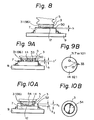
- Figure 3 shows a third embodiment of the present invention, in which the first heat transfer plate 3 is provided with protrusion 33 on the bottom face 14 thereof, which protrusions 33 constitute projections for limiting downward movement of the first heat transfer plate 3 relative to the circuit component 7, so that the plate 3 and the component 7 can be maintained constant.
- the second solder 31 which is located on the circuit component 7 and is melted by the heat dissipated from the tip 6 of the component 7, is maintained between the first heat transfer plate 3 and the component 7 without leaking out from therebetween.
- the low melting second solder 31 tends to be squeezed from between the plate 3 and the component 7 in the outward direction when downward pressure is exerted on the plate 3 by the bellows 5. This tendency can be eliminated by the provision of the projections 33 between the bottom surface. i.e., the heat absorbing surface 14 of the plate 3, and the circuit component 7 or the second plate 10, if any. Accordingly, the protrusions 33 can be provided on the circuit component 7 or the second plate 10 in place of on the first plate 3. Note, the height H of the projections 33 is determined in accordance with the necessary amount of the second solder 31.
- the protrusions 33 have flat bottom surfaces 34 to realize a stable contact of the protrusions 33 with the upper surface 12, i.e. heat radiation surface, of the component 7.
- the three protrusions 33 are illustrated in this embodiment but the number thereof is not limited.
- the three protrusions 33 are arranged at an equicircumferential distance in the form of, for example, a tripod, to ensure a stable location of the plate 3 on the component 7 or the plate 10.
- the projections which are embodied, for example, by the protrusions 33, also contribute to an increase in the contact pressure of the second solder 31 against the circuit component 7 when the plate 3 moves downward, and accordingly, to cause the second solder 31 to melt from the center thereof.
- the second solder 31 is maintained between the plate 3 and the component 7 not only by the protrusions 33 but also by its own interfacial tension.
- the protrusions 33 in Fig. 3 are replaced by a semi-spherically curved bottom surface 36 which is convexed toward the heat radiation surface 12 of the component 7.
- the height H of the crown i.e. the convex of the surface 36, is same as the height H of the protrusions 33 in Fig. 3.
- the curved surface 36 can be provided on the component 7 (or the plate 10 in Fig. 1) in place of the plate 3.
- the second solder 31 can be maintained between the first plate 3 and the component 7 around the top of the crown formed by the curved surface 36, due to its own interfacial tension.
- the second solder 31 may contain or produce air bubbles therein, and accordingly, when the second solder 31 is melted by the heat, the bubbles will be maintained in the second solder 31. These bubbles decrease the efficiency of the heat transmission between the first heat transfer plate 3 and the circuit component 7.
- the first heat transfer plate 3 has. on the bottom surface 14 thereof, recessed grooves 38 which are arranged in a grid-like manner and which have a generally V-shaped cross section.
- the grooves 38 provide a passage for discharging the air bubbles in the second solder 31.
- the gas discharging passage can also be formed by a plurality of radially extending recessed grooves 40 as shown in Figs. 6A and 68.
- the grooves 40 have a generally trapezoidal cross section.
- the cross section of the recessed grooves 30 or 40 is not limited to those illustrated in Figs. 5A and 6A. but can be of any other shape. Also, the arrangement of the recessed grooves 38 or 40 is not limited to the grid-like or radial arrangement shown in Figs. 5A or 6A.
- the recessed grooves 38 or 40 can be machined or cut by a mechanical cutter or cutting machine (not shown), or they can be made by, for example. an optical means, such as a laser cutter.
- predetermined recessed grooves 44 can be automatically formed when the second solder 31 is formed between the first heat transfer plate 3 and the circuit component 7 or the second heat transfer plate 10, if any. The air bubbles which would otherwise remain in the second solder 31 can be thus discharged outside through the recessed grooves 38, 40, or 44.
- the gas discharging passage can be provided on the circuit component 7 or on the second heat transfer plate 10, if any, instead of on the first heat transfer plate 3.
- the recessed grooves 38, 40, or 44 can be formed on the upper surface of the heat transfer plate 10 or circuit component 7 adjacent to the second solder 31.
- the second solder 31 can be at least partially maintained between the plate 3 and the component 7 or the plate 10 because of the interfacial tension thereof. as mentioned above. Nevertheless, the second solder 31 when molten tends to flow, or to be squeezed from between the plate 3 and the component 7 or the plate 10, if any, due to its flowability, particularly when downward pressure is exerted on the second solder 31 by the bellows 5 through the plate 3.
- means for maintaining the second solder 31 between the plate 3 and the plate 10 or the component 7 is provided therebetween.
- the component 7 has an annular circumferential wall 50 on the upper surface 12.
- the wall 50 is made of material which has no solder wetting property, such as a solder resist, so that the second solder 31 does not adhere to the wall 50.
- the wall 50 has a height h which is determined in accordance with the necessary amount of second solder 31 enclosed in the wall 50.
- the plate 3 comes into contact with the wall 50 to define a closed s h :rce for the second solder 31 between the plate 3 and the component 7 or the plate 10, if any.
- the wall 50 prevents the second solder 31 from leaking out therefrom or from being squeezed out therefrom. If the second solder 31 leaks out onto the circuit plate 9, short-circuits or malfunctions of the circuit components or wiring on the plate 9 may occur.
- the protrusions 33 which are similar to those shown in Fig. 3, are provided on the bottom surface 14 of the plate 3. in addition to the circumferential wall 50 of the component 7.
- the height h' of the protrusions 33 is higher than the height h of the wall 50.
- the protrusions 33 limit the downward movement of the plate 3. Namely, the protrusions 33 can provide a precise gap between the plate 3 and the component 7 or the plate 10, if any.
- the solder 31 can be maintained between the plate 3 and the component 7 or the plate 10 due to interfacial tension. It is also possible to provide the protrusions 33 on the component 7 or the plate 10, if any, instead of on the plate 3.
- the protrusions 33 in Fig. 9A are replaced with a single large projection 54 having a generally trapezoidal cross section and provided on the plate 3.
- the projection 54 has a height h2 which is smaller than a height h1 of the circumferential wall 52 provided on the component 7 or the plate 10, if any.
- the wall 52 comes into contact with the bottom surface 14 of the plate 3, so that there is a small gap between the bottom of the projection 54 and the upper surface 12 of the component 7, which gap can be filled with the second solder 31. Since the projection 54 is completely embedded in the second solder 31, a better thermal contact between the plate 3 and the component 7 can be realized.
- a completely enclosed space is provided in the wall 52 when the wall 52 comes into contact with the plate 3, so that the second solder 31 can be completely enclosed in the enclosing space.
- the heights h1 and h2 can be determined in accordance with the necessary amount of second solder 31 to be enclosed in the enclosed space.
- the circumferential wall 50 is provided on the plate 3, instead of on the component 7.
- the arrangement shown in Fig. 11 functions in the same manner as the embodiment shown in Fig. 8.
- the separation of the first heat transfer plate 3 from the component 7 or the second heat transfer plate 10, if any, or the disassembly of the cooling module is sometimes necessary for, for example, design modification or repair, etc. Accordingly, an easy separation of the first heat transfer plate 3 from the component 7 or the second plate 10 is desirable.
- the separation is effected when the second solder 31 is in a molten state.
- a hot liquid 60 is circulated in the passage 1 and the recirculation line 23 (see also Fig. 1). Namely, when it is necessary to melt the second solder 31 in order to separate the plate 3 from the component 7 or the plate 10, if any, a hot liquid, such as hot water, is circulated in the recirculation line 23. The plate 3 is heated by the hot liquid 60, so that the second solder 31 can be melted.
- the second solder 31 When the second solder 31 has a low-melting-point, it can be melted at a temperature below 100°C, as mentioned above
- the melting point of the second solder 31 depends on the amount of the additive. such as bismuth, to be added to the solder, which is usually made of tin and lead, as mentioned before. Boiling water can be used as the hot liquid or a hot gas can be used instead.
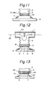
- a heater in the first plate 3, as shown in Fig. 13.
- the plate 3 is hollow and is provided with a heater 63 therein.
- the heater 63 can be a conventional electric heater.
- two terminals 65 extend outside from the plate 3, so that these terminals 65 can be easily connected to a power source (not shown) only when necessary.
- the heating is preferably effected after the coolant 2 is removed from the passage 1. and accordingly, from the recirculation line 23.
- the solder 31 can be melted through the plate 3 by a simple heating process.
- Figure 14 shows a series of cooling modules (three modules in the illustrated embodiment), in which each module corresponds to the cooling module shown in Fig. 2.
- the passage 1 is constructed by a lower half 1A and an upper half 1 B.
- the lower half 1A has, for example, a generally U-shaped cross-section, and has openings 73 connected to the recirculation zones 32 of the cooling modules.
- the upper half 1 B can be fitted onto the lower half 1A to define an outlet passage 81.
- the upper half 1 B therefore, acts as a cover of the passage for the coolant 2.
- the upper half 1 B has an upper inlet passage 83 which corresponds to the passage 1 in Fig. 2.
- the passage 83 is connected to the outlet passage 81 by nozzles 85. so that the coolant 2 fed through the recirculation line 23 can be fed or ejected onto the heat transfer plates 3 of the cooling modules through the nozzles 85 and is recirculated to the recirculation line 23 through an outlet passage 81 and an outlet pipe 88 provided on the upper half 1 B of the passage 1.
- the coolant 2 can be introduced into the inlet passage 83 from an inlet pipe 89 provided on the upper half 1B.
- the upper half 1B can be detachably connected to the lower half by, for example, bolts 71.
- the numeral 70 designates a seal, such as a ring packing, or a gasket which is located between the upper and lower halves 1A and 1B to seal the connection therebetween.
- Figure 17 shows one example of a perspective appearance of a cooling unit having a series of cooling modules shown in Fig. 14.
- the inlet pipe 89 and the outlet pipe 88 are in different positions from those shown in Fig. 14.
- the first heat transfer plates 3 are separated from the corresponding circuit components 7 on the printed circuit board 9.
- the second solder 31 (not shown) is held, for example, on the corresponding components 7 with the help of the circumferential wall 50 (Fig. 8).
- the cover 1B can be detached from the lower half 1A by removing the bolts 71.
- Figure 15 shows a heater unit 90 having a heater block 92 provided with a number of heater 91 corresponding to the number of cooling modules.
- the heaters 91 are supported in heater supports 94 which, in turn, are supported by the heater block 92 by springs 93.
- the heater supports 94 can move up and down.
- the heaters 91 can be conventional electrical heaters similar to the heater 63 shown in Fig. 13.
- the heater unit 90 can be located on the cooling modules, after the cover 1B of the passage 1 is removed, as shown in Fig. 16. When the heater unit 90 is located on the cooling modules, the heater supports 94, and accordingly the heaters 91, are pressed against the plates 3 of the corresponding cooling module by the springs 93.
- the heating by the heaters 91 can be controlled by a controller 100 electrically connected to the heater unit 90, so that it is possible to heat only one or several of the cooling modules in which the second solder 31 must be melted. It is also possible to heat all the cooling modules at one time.
- the springs 93 can be dispensed with, since the heater supports 94 are pressed against the plates 3 by the dead weight thereof.
- the melting of the second solder 31 of the cooling modules can be easily carried out only by replacing the cover 1B of the passage 1 for the coolant with the heater unit 90.
- Figure 18 shows a cooling module according to another aspect of the present invention, in which the first heat transfer plate 3 is thermally connected to the circuit component 7 by a metal plate 92 having a high thermal conductivity.
- the second solder 31 shown in the preceding drawings is replaced with the conductive metal plate 92 in Fig. 18.
- the metal plate 92 can be connected to the first heat transfer plate 3 by an adhesive or a mechanical fastening means (not shown).
- the metal plate 92 has a number of small cells or cavities, i.e. it is porous, as shown in Fig. 19.
- the metal plate 92 contains a low-melting-point metal 96 (Fig. 19) impregnated therein.
- the porous metal plate 92 can be made by compressing a foamed metal or metal mesh.
- the low-melting-point metal 96 is made, for example, of an alloy or alloys of two or more of gallium (Ga), indium (In), and tin (Sn), and the like, which can be melted at a temperature of. for example, 40°C - 120°C.
- the low-melting-point metal 96 is preferably solid in the normal state, i.e., without heating, and is molten when heated at a temperature higher than, for example, 40 c C.
- the metals, Ga, In, Sn can be easily oxidized in the atmosphere and, accordingly, are preferably used in an environment not containing oxygen.
- the low-melting-point metal 96 is impregnated in the small cells or cavities of the porous metal plate 92.
- the low-melting-point metal 96 impregnated in the metal plate 92 is melted and liquidized, so that the low-melting-point metal 96 comes into compliance contact with the circuit component 7 or the second plate 10, if any, resulting in a complete thermal contact between the first plate 3 and the component 7 or second plate 10 through the metal plate 92.
- liquidized low-melting-point metal 96 can be maintained between the plate 3 and the component 7 or the second plate 10, if any, without leaking out from therebetween, due to the interfacial tension thereof.
- the separation of the first plate from the component 7 or the second plate 10, if any, can be easily carried out when the cooling module is not operating, namely, when the circuit device is not operative.
- the coolant 2 can be ejected onto the first heat transfer plate 3 through the nozzle 85, similar to the aspect shown in Fig. 14.
- the bellows 5 can be secured to the passage 1 by a flange 82 connected to the bellows 5 through an O-ring 80, which seals the connection between the flange 82 and the passage 1.
- the low-melting-point metal 96 which is impregnated in the metal plate 92 and which is liquid in the normal state, I.e.. without heating.
- the low-melting-point metal 96 has a melting point below or within the environment temperature range in which the cooling module and the circuit device operate.
- the low-melting-point metal which is liquid even at the environment temperature is impregnated in the metal plate 92, the latter can be cooled below the melting point of the low-melting-point metal 96 to make it solid when the first plate 3 is separated from the component 7 or the second plate 10, if any. Namely, since it is necessary to solidify the low-melting-point metal 96 to separate the heat transfer plate 3 from the component 7, the low-melting-point metal 96 must be cooled to a temperature at which the low-melting-point metal 96 is solidified.
- the low-melting-point metal 96 directly held in and by the first heat transfer plate 3.
- the bottom surface 14 of the plate 3 is provided with a circumferential wall or flange 3a which comes into contact with the component 7.
- the flange 3a has an annular projection 3b extending inward to provide a generally T-shaped space in the plate 3, so that the low-melting-point metal 96 can be held in and by the plate 3 even when the plate 3 is separated from the component 7, so long as the metal is in a solid state.
- the low-melting-point metal 96 should be solid.
- seal member 103 such as an O-ring, gasket or packing to prevent the liquidized low-melting-point metal 96 from leaking out from the connection between the component 7 and the wall 3a of the plate 3.
- the seal member 103 can be secured to the flange 3b and/or the wall 3a of the plate 3.
- the low-melting-point metal 96 expands in volume when heated by the heat from the component 7, that is, when it is liquidized, and preferably a means is provided for absorbing this expansion.
- a cavity or space 107 is provided between the low-melting-point metal 96 and the wall 3a of the plate 3, as shown in Fig. 21.
- the space 107 can absorb the expansion of the low-melting-point metal 96. Namely, when heated, the low-melting-point metal 96 can expand into the space 107.
- a part or all of the side peripheral portion of the wall 3a is formed by an elastic sheet or sheets 109 connected thereto, which can deform outward in the direction designated by an arrow, substantially perpendicular to the direction of the spring force of the bellows 5, as shown by an imaginary line in Fig. 22.
- the deformation of the sheet(s) 109, as shown at 109' absorbs the expansion of the low-melting-point metal 96.
- a circumferential wall 7a having a flange 7b on the component 7 instead of on the plate 3, as shown in Fig. 23.
- the seal member 103 is provided between the plate 3 and the flange 7b of the component 7.
- the low-melting-point metal 96 can be held in the circumferential wall 7a and on the component 7.
- Figs. 3, 4,5B, 6B, 7,8,9A, 10A, and 11 can be combined with the embodiment shown in Fig. 18 or 20, in which the second solder 31 is replaced with the low-melting-point metal 96.
- This alternative is designated in those drawings by a parenthesized numeral (96) after the numeral 31.
- the upper surface 12 of the component 7 (or the upper surface of the second plate 10, if any) can be coated with, for example, fluorinated plastic resin 93 (Fig. 18), such as Teflon 0 , so that the low-melting-point metal 96 can be easily separated from the coated surface 12 when the low-melting-point metal 96 is solidified to separate the plate 3 from the component 7.
- fluorinated plastic resin 93 Fig. 18
- Teflon 0 Teflon 0
- the bottom surface 14 of the plate 3 can be coated with a similar material for the same purpose.
- a means for increasing the contacting surface area between the coolant 2 and th first heat transfer plate 3 is provided, as shown in Figs. 24 to 30.
- the plate 3 is provided with a substantially cylindrical tubular plate 110 integral therewith into which the lower end, i.e., the front end, of the nozzle 85 is inserted.
- the tubular plate 110 is located in the bellows 5.
- the tubular plate 110 increases the contacting surface area between the plate 3 and the coolant 2.
- the coolant ejected from the nozzle 85 comes into collision with the plate 3 and flows up along the tubular wall of the plate 110, removing the heat from the plate 3, as shown by arrows in Fig. 24.
- the tubular plate 110 can be provided, on its inner periphery, with heat radiation fins 111, as shown in Fig. 25. As is well known, such fins 111 will increase the heat transmission efficiency between the tubular plate 110 and the coolant 2.
- the fins 111 are preferably arranged in a concentrical arrangement as shown in Fig. 25, so that the radially extending fins 111 do not substantially interrupt the smooth flow of the coolant 2.
- tubular plate 110 in Fig. 24 is replaced with a cylindrical tubular plate 120 having a corrugated cylindrical wall.
- the heat transmission effect can be increased in comparison with the plain cylindrical wall as shown in Fig. 24.
- the bellows Since the coolant 2 substantially does not come into direct contact with the bellows 5, because of the presence of the tubular wall or the tubular plate 110 or 120, which has a height substantially equal to the length of the bellows 5, the bellows, which is usually made of a thin metal plate, can be protected from collision of the coolant 2 thereagainst, resulting in the prevention of possible corrosion or of damage to the bellows.
- Figures 27 and 28 show another embodiment of the tubular construction provided on the plate 3.
- a plurality of plate-like fins 130 are provided on the plate 3.
- the fins 130 are discontinuously arranged along a circle and radially extend when viewed in section in Fig. 27. Since the fins 130 are spaced from one another preferably at an equidistance, the resistance against the flow of the coolant 2 can be decreased in comparison with the continuous cylindrical wall as shown in Fig. 24.
- Fig. 29 which shows a variant of the fins 130 shown in Fig. 28, the fins 140 have a streamline shape in section, from the viewpoint of aerodynamics. to decrease the resistance of the fins 140 to the smooth flow of the coolant 2.
- FIG. 30 shows a cooling module according to another aspect of the present invention.
- the hellows 5 is directly connected to the first heat transfer plate 3, which has a larger diameter than that of the bellows.
- the peripheral end of the plate 3 is guided by guide rods 160 which will be described hereinafter.
- Figure 31 shows a different embodiment of Fig. 30.
- a cylindrical tubular plate 150 similar to the tubular plate 110 in Fig. 24 is connected to the bottom end of the bellows 5, which is smaller in diameter than the tubular plate 150.
- the plate 3 has a cylindrical tubular shape with an open end and a closed bottom to provide the tubular wall 150, which is defined by the side peripheral wall of the cylindrical plate 3.
- the tubular wall 150 has a larger surface area than that of the tubular wall 110 in Fig. 24, which can be understood when the diameters of the cylinders are taken into consideration, an increased heat transmission effect can be expected.
- guide rods 160 are provided around the plate 3 (Fig. 30) or the tubular wall 150 of the plate 3 (Fig. 31) to prevent the plate 3, and accordingly the wall 150, from being inclined with respect to the horizontal and thus the plane of the component 7, as can be seen in Fig. 32.
- the guide rods 160 extend vertically downward from the passage 1 in recesses 151 provided on the tubular wall 150.
- the guide rods 160 also contribute to prevention of undesirable and accidental movement by the plate 3 during operation of the cooling modules. Furthermore, the guide rods 160 guide the downward movement of the plate 3 when it is located on the component 7.
- the guide rods 160 can be replaced with guide plates 170 which have an arced section extending along the cylindrical wall 150. and which surround the cylindrical wall 150 as shown in Fig. 33.
- the recesses 151 shown in Fig. 31 can be omitted.
- the plate 3 or tubular wall 150 are larger than that the bellows 5, the latter, which has usually a very small thickness, can be prevented coming into undersirable contact or collision with the guide rods 160 or 170.
- the number of the guide rods is not limited to four, only three guide rods 160' can be provided, as shown by imaginary lines in Fig. 32.
- three recesses 151' can be provided at a 120" spacing. More than four guide rods can be also provided.
- a compound or compounds 180 having a high heat conductivity can be inserted between the lower end(s) of the guide rod(s) 160 and 170 and the corresponding component(s) 7'.
- the compound(s) 180 can serve as a spacer to adjust the distance between the lower end(s) of the guide rod(s) 160 and 170 and the component(s) 7'.
- the guide rod(s) 160 and 170 should be made of a material having a high heat conductivity, such as copper.
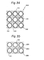
- Figure 34 shows a guide assembly 200 which entirely guides a series of tubular walls 150 of the cooling modules (also see Figs. 14 and 17).
- the guide assembly 200 is constructed by blocks 201 each having a round cross shape in section and defining, together with adjacent blocks, openings 202 corresponding to the plates 3 or the tubular walls 150 thereof.
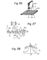
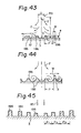
- a means is provided for producing turbulence in the flow of the coolant 2. as shown in Figs. 36 to 45.
- the plate 3 is provided with a plurality of parallel ridges 182.
- the ridges 182 extend in parallel to the length of the rectangle formed by the nozzles 85.
- This turbulence causes a disturbance in the flow of the coolant 2 flowing along the heat transmission surface 12 therefrom, resulting in a production of vortexes in the flow of the coolant 2, as can be seen in Fig. 37.
- the vortexes locally increase the heat conductivity.
- the flow of the coolant 2 disturbed from the laminar flow and forming the vortexes again comes into collision with the surface 12 at a point RL.
- the heat conductivity can be thus increased locally, particularly at the point RL. at which the flow comes into contact again with the plate 3.
- the solid line C1 represents the present invention in which the ridges 182 are provided on the plate 3 and the dash-dot line C2 represents the prior art in which ridges are not provided on the plate 3 (flat surface plate), respectively.
- the ridges 182 increase the heat conductivity even in the portion far from the center point 0.
- the heat conductivity is high only at or near to the center point 0.
- the ridges 182 provide a uniform distribution of the heat conductivity over the entire surface of the plate 3.
- the curve C1 varies in accordance with the distance L between the lower end of the nozzle 85 and the heat transmission surface 12 of the plate 3, the width w of one ridge 182, the height e of the ridges 182, and the pitch E of the ridges 182.
- Figure 39 to 41 show another embodiment of the invention, in which the plate 3 has a plurality of annular ridges 186 coaxial to each other on the heat transmission surface 12.
- the ridges 186 have a rectangular cross section.
- the plate 3 is circular in plan view.
- the nozzle 85 which has a circular cross section, is located directly above the center of the innermost annular ridge 186.
- the heat conductivity slightly decreases as the distance from the center point 0 of the surface 12 increases. Accordingly, if the ridges are annular as shown in Fig. 40, each ridge has the same distance x from the center point 0, and accordingly, a more uniform distribution of a higher heat conductivity can be expected from the arrangement shown in Figs. 39 to 41.
- the ridges 186 also contribute to an increase of the area of the surface of the plate 3 in contact with the coolant 2, resulting in an increase of the cooling effect.
- each ridge 186 need not always be a complete circle but can be discontinuous with a gap or gaps, as shown in Fig. 42.
- each of the annular ridges 186 in Fig. 40 are replaced by separate discontinuous annular ridges 186'.
- each annular ridge 186' has a small gap 187 to define a discontinuous annular ridge.
- the gaps 187 are preferably deviated from each other for each ridge, in the circumferential direction.
- the coolant 2 ejected from the nozzle 85 comes into collision with the center portion of the surface 12 of the plate 3 between the innermost ridges 186 (or 186') and spreads along the ridges 186 (or 186').
- the same phenomena takes place at each of the ridges 186 (or 186') and the vortexes occur as shown in Fig. 43.
- round recesses 188 having a semicircular cross section between the annular ridges 186 (or 186'), as shown in Fig. 44.
- the round recesses 188 assist the production and the maintenance of the vortexes.
- Figure 45 shows an alternative arrangement of the annular ridges 186 or 186', in which the ridges have different pitches and different heights.
- the pitches vary so that the pitch between the innermost ridge and the adjacent ridge is smallest and the pitch increases toward the outer ridges.
- the heights vary, so that the height of the innermost ridge is smallest and the height increases toward the outer ridges.
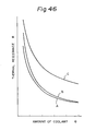
- Figure 46 shows an experimental result of three products.
- the first product A is that shown in Fig. 44, which has the round recesses 188 between the annular ridges 186;
- the second product B is that shown in Fig. 43, which has the annular ridges 186 and the flat surface portions between the ridges;
- the third product C is that which has not ridges and which is the same as that used in the experiment shown in Fig. 38 and represented by the curve C2.
- the diameter D of the nozzle 85, the width w of the ridge 186, the height e of the ridge 186, and the pitch p of the ridges 186 had the following relationship:
- the axis of the ordinates designated by R represents the thermal resistance between the coolant 2 and the heat transmission surface 12 of the plate 3, and the axis of the abscissas designated by Q represents the amount of the coolant 2. It will be understood that the thermal resistance R can be decreased by about one half by the providion of the ridges 186, when the amount of coolant is relatively large.
- round recesses 188 contribute to a decrease of the thermal resistance R.
- w, e, p depend on the values of L and D.
- e/D 1/20 - 1/3
- p/e 3 - 10
- w/e 1, for the embodiment shown in Fig. 43
- p/D 0.2 - 2
- w/d 1/20 - 1/3, for the embodiment shown in Fig. 44, respectively;
- the potential core is UD $ 6 - 8
- the cooling apparatus can be used upside down, so that the coolant is ejected upward from the nozzles 85 toward the heat transfer plates 3 located above the nozzles 85.
- the allowable heat transfer between the first heat transfer plate and the circuit component or the second heat transfer plate, if any, can be increased and the thermal contact resistance therebetween can be decreased, resulting in a high heat transfer ratio and a high cooling efficiency.
- the first heat transfer plates can be easily disconnected from the circuit components or the second heat transfer plates, if any, merely by melting the second solder or by solidifying the low-melting-point metal, between the first heat transfer plates and the circuit components or the second heat transfer plates.
- the second solder or the low-melting-point metal can be maintained between the two heat transfer plates or the transfer plates and the circuit components without leaking out from therebetween.
Abstract
Description
- The present invention relates to a cooling system for an electronic circuit device. More particularly, it relates to a printed circuit board holding electronic circuit components, such as semiconductors, large scale integrated circuits (LSI's), or integrated circuit (IC's), wherein these components are cooled by a cooling system that includes a cooling module or a series of cooling modules for removing the heat dissipated from the component and transferring it to a coolant flowing in a passage.
- In previously-proposed cooling modules for an electronic circuit device, a heat transfer element such as a heat transfer plate or a heat sink head is placed on the circuit components, such as IC's, LSI's, and semiconductors, by pressure from a spring or a bellows, to remove the heat dissipated from these circuit components. The heat transfer elements are exposed to a coolant (usually a gaseous coolant), in such a manner that the heat removed from the circuit components is transferred to the coolant by the corresponding heat transfer element.
- Located between the heat transfer plate and the circuit component is a deformable or elastic thermal conductive sheet, such as a thermal sheet, and a second heat transfer plate can be located between the thermal sheet and the circuit component to be cooled. The thermal sheet usually consists of, for example, silicone-containing material such as silicone rubber having incorporated therein metal or an oxide thereof, such as alumina, beryllia to increase thermal conductivity and to bind the plastic material. The heat transfer between the first heat transfer plate and the corresponding circuit component can be effected through the thermal sheet (and the second heat transfer plates, if any).
- Since, however, the thermal sheet is made of a soft plastic material as a matrix material, although mixed with metal powders having a high heat conductivity, the heat conductivity is still relatively small. It is impossible to increase the amount of metal component inclusion, as this will decrease the elasticity of the thermal sheet. Furthermore, since the thermal sheet is solid, although elastic, a complete surface contact between the first heat transfer plate and the circuit component or between the first and second heat transfer plates can not be achieved if there is any unevenness or distortion on the contacting surfaces of the first or second heat transfer plate or the circuit component. This incomplete surface contact results in a large and non-uniform thermal contact resistance, and any change in the pressure from the spring or bellows leads directly to a change in the thermal contact resistance, resulting in an unstable thermal contact resistance. These factors cause a large loss in the heat transfer efficiency.
- It is accordingly desirable to provide a cooling system for an electronic circuit device which can effectively, stably, and uniformly cool the circuit components.
- In an embodiment of the present invention, the previously-proposed thermal sheet is replaced by a solder which has a flowability when heated, that is, the solder is liquidized when heated above a predetermined temperature.
- With this arrangement, the first heat transfer plate can be adhered to the circuit component or the second heat transfer plate provided on the circuit component, in a compliant or rigid contact fashion.
- Namely, the flowable solder spreads over the entire contacting surfaces between the first heat transfer plate and the circuit component or the second heat transfer plate, so that a substantially complete surface contact therebetween can be achieved regardless of any surface evenness of the contacting surfaces.
- According to another embodiment of the present invention, the thermal sheet is replaced with a low-melting-point metal which can be melted by the heat from the circuit component.
- Means for preventing the molten metal from leaking from between the edges of the contacting surfaces of the first heat transfer plate and the circuit component or the second heat transfer plate can be provided.
- Also, according to a further embodiment of the present invention, there is provided a means for increasing the contacting surface area between the first heat transfer plate and the circuit component or the second heat transfer plate.
- According to still another embodiment of the present invention, there is provided a means for producing a turbulence in the flow of the coolant to which the first heat transfer plate is exposed to increase the heat transfer efficiency.
- Reference will now be made, by way of example, to the accompanying drawings, in which:
- Fig. 1 is a schematic sectional view of a cooling system embodying the present invention;
- Fig. 2 is a schematic sectional view of a second cooling system embodying the present invention;
- Fig. 3 is a schematic sectional partial view of a third cooling system embodying the present invention;
- Fig. 4 is a view similar to Fig. 3 but showing a variant thereof;
- Figs. 5A and 5B are a partial cross sectional view and a plan view of a contacting surface of a first heat transfer plate;
- Figs. 6A and 6B are views similar to Figs. 5A and 5B, respectively, but showing a different embodiment of the present invention;
- Fig. 7 is a partial cross sectional view of a contacting surface of a first heat transfer plate embodying the present invention;
- Fig. 8 is a partial sectional view of a fourth cooling module embodying the present invention;
- Fig. 9A is a partial sectional view of a variant of Fig. 8;
- Fig. 9B is a bottom view of a first heat transfer plate shown in Fig. 9A;
- Fig. 10A is a view showing a modified variant of Fig. 9A;
- Fig. 10B is a bottom view of a first heat transfer plate shown in Fig. 10A;
- Fig. 11 is a partial sectional view of a fifth cooling module embodying the present invention;
- Fig. 12 is a partial cross sectional view of a sixth embodiment of the present invention;
- Fig. 13 is a partial view showing a variant of Fig. 12;
- Fig. 14 is a schematic sectional view of a series of cooling modules embodying the present invention;
- Fig. 15 is a schematic view of a heater unit for use in an embodiment of the present invention;
- Fig. 16 is a schematic view of a series of cooling modules having a heater unit illustrated in Fig. 15;
- Fig. 17 is a perspective view of a cooling unit having a series of cooling modules shown in Fig. 14;
- Fig. 18 is a partial sectional view of a seventh cooling module embodying the present invention;
- Fig. 19 is an enlarged partial sectional view of a metal plate shown in Fig. 18;
- Fig. 20 is a partial sectional view of a variant of Fig. 18;
- Fig. 21 is an enlarged view of a part of Fig. 20 but showing a modification thereof;
- Fig. 22 is a view similar to Fig. 21 but showing a variant thereof;
- Fig. 23 is an enlarged partial view similar to Fig. 20, but showing a modified embodiment;
- Fig. 24 is a cross sectional view of a cooling module according to another aspect of the invention;
- Fig. 25 is a plane view showing a variant of a tubular plate;
- Fig. 26 is a sectional view of still another modification of a tubular plate;
- Fig. 27 is a cross sectional view of an eighth cooling module embodying the invention;
- Fig. 28 is a sectional view taken along the line XXVIII-XXVIII in Fig. 27;
- Fig. 29 is a sectional view showing a variant of Fig. 28;
- Fig. 30 is a cross sectional view of a ninth cooling module embodying the present invention;
- Fig. 31 is a sectional view showing a variant of Fig. 30:
- Fig. 32 is a schematic plan view of a tubular wall of a heat transfer plate and guide rods shown in Figs. 30 and 31;
- Fig. 33 is a view similar to Fig. 32, but showing a variant thereof;
- Fig. 34 is a view similar to Fig. 32 but showing still another variant thereof;
- Fig. 35 is a view showing another modification of Fig. 34;
- Fig. 36 is a schematic perspective view of a nozzle and ridges provided on the heat transfer plate, embodying a different aspect of the present invention;
- Fig. 37 is a cross sectional view of Fig. 36. for explaining how turbulence occurs in the coolant;
- Fig. 38 is a diagram showing a relationship between the heat conductivity and a distance from a center point of the heat transfer plate directly below the nozzle, and comparing effects caused by the presence or absence of ridges on the heat transfer plate;
- Fig. 39 is a cross sectional view of another embodiment of a cooling module different from Fig. 36;
- Fig. 40 is a plan view of a heat transfer plate having annular ridges;
- Fig. 41 is a cross sectional view of the ridges shown in Fig. 40;
- Fig. 42 is a plan view of a variant of ridges shown in Fig. 40;
- Fig. 43 is a cross sectional view for explaining how the turbulence of the coolant is caused by the ridges shown in Fig. 39;
- Fig. 44 is a view showing a modified heat transfer plate with annular ridges and round recesses therebetween;
- Fig. 45 is a sectional view of annular ridges having different pitches and heights; and,
- Fig. 46 is a diagram showing experimental results of a relationship between the thermal resistance and the amount of coolant, depending on the presence or absence of the ridges, and also depending on the presence or absence of the round recesses between the ridges.
- Figure 1 shows an embodiment of the present invention in which the cooling module has a
passage 1 for the coolant flow. - The coolant can be gas but is not limited thereto, and may be a liquid, such as water, liquid fluorocarbon, or even a liquid metal such as mercury or gallium. The
passage 1 is preferably a part of arecirculation line 23 having therein apump 29 and a heat radiator orheat exchanger 25. - A first
heat transfer plate 3 which is made of, for example, a heat conductive material, such as copper or brass, is connected to thepassage 1 by means of abellows 5 attached to thepassage 1. Thebellows 5 is usually made of a thin sheet of copper or stainless steel. Thepassage 1 has, preferably, adeflector 21 extending toward the firstheat transfer plate 3. Acoolant recirculation zone 32 is defined in thebellows 5, in which zone 32 the firstheat transfer plate 3 is exposed to the coolant at one side face of theplate 3. - The direction of the coolant flow in the
passage 1 is changed by thedeflector 21, which can be dispensed with, and thus the heat is removed from the firstheat transfer plate 3 in thecirculation zone 32. - The
plate 3 is pressed against anelectronic circuit component 7, such as an IC, LSI, or semiconductor provided on a printedcircuit board 9, by means of thebellows 5 and the hydraulic pressure of the coolant. - The
component 7 is bonded to the printedcircuit board 9 by, for example,solder 11. - The
component 7 illustrated in Fig. 1 has atip 6 and apackage 8. - In the illustrated embodiment, a second
heat transfer plate 10 is adhered to and on thecomponent 7 by, for example, soldering or die bonding. The firstheat transfer plate 3 forms a heat sink head. The secondheat transfer plate 10 has a large area thantip 6, and thus the heat transfer surface thereof is large. - According to an embodiment of the present invention. an intermediate layer of
solder 31 is provided between the first and the secondheat transfer plates - In the illustrated embodiment, the
intermediate layer 31 is secured to the bottom side face of the firstheat transfer plate 3. Alternatively, theintermediate layer 31 can be secured to thecircuit component 7 on the printedcircuit board 9. - The
solder 31 maintains its original sheet like shape at a normal temperature, i.e. when the circuit device is not in operation. When the circuit device is operated and, consequently, thetip 6 produces heat, thesolder 31 is melted so that the first and the secondheat transfer plates solder 31. Thus, the twoplates plates - Thus, in an embodiment of the present invention, cooling efficiency of the cooling module is increased, because the
second solder 31 ensures a thermal connection between the first and the secondheat transfer plates - Preferably, the solder 31 (referred to as the second solder hereinafter) has a low melting point T2 which is lower than a melting point T1 of the solder 11 (referred to as the first solder hereinafter). Namely T1 > T2.
- Preferably the difference between the melting points T1 and T2 is in the range of 40°C to 200°C. Namely. T1 - T2 = 40° C - 200° C.
- Due to the difference between the melting points T1 and T2, the
first solder 11 does not melt at a temperature at which thesecond solder 31 becomes molten. This means that when the cooling module is located in an atmosphere having, for example, a temperature at which thesecond solder 31 melts but thefirst solder 11 does not, thesecond solder 31 is melted in order to separate the firstheat transfer plate 3 from the secondheat transfer plate 10, but the connection between thecircuit component 7 and the printedcircuit board 9 is maintained as it is by thefirst solder 11. - The removal or separation of the first heat transfer plate from the second
heat transfer plate 10 is necessitated when, for example, thetip 6 of thecomponent 7 is replaced with another or modified in accordance with a design modification, or thetip 6 does not work and must be replaced or repaired. - The melting point of the
second solder 31 can be decreased to 85°C ~ 100°C by adding, for example, bismuth. to a conventional solder having tin and lead as the main components. - The
first solder 11 can be a eutectic solder which has, for example. a melting point of about 185° C. - Figure 2 shows a variant of Fig. 1. In the arrangement illustrated in Fig. 2. the second
heat transfer plate 10 of Fig. 1 is omitted. Namely, thesecond solder 31 is allowed to achieve a direct thermal connection between the firstheat transfer plate 3 and thecircuit component 7. - The melting point T2 of the
solder 31 is preferably within an operation range of thecorresponding circuit component 7, that is, below a temperature at which thecircuit component 7, especially thetip 6, might malfunction, so that when the device is located in an atmosphere having a relatively high temperature, to melt thesolder 31 and separate theplate 3 from thecomponent 7 as mentioned above, thecircuit component 7 will not accidentally malfunction. - Apart from the absence of the second heat transfer plate, the embodiment shown in Fig. 2 functions in the same manner as the embodiment illustrated in Fig. 1.
- As can be seen from the foregoing description, in an embodiment of the present invention, when molten the
second solder 31 ensures a full compliant contact with the twoplates 3 and 10 (Fig. 1) or the firstheat transfer plate 3 and the circuit component 7 (Fig. 2), even when theplate 3 and/or thecircuit component 7 or the secondheat transfer plate 10 have uneven or irregular contacting surfaces. Thesecond solder 31 also contributes to an easy separation of the firstheat transfer plate 3 from thecircuit component 7 or the secondheat transfer plate 10. - The
plates - Figure 3 shows a third embodiment of the present invention, in which the first
heat transfer plate 3 is provided withprotrusion 33 on thebottom face 14 thereof, which protrusions 33 constitute projections for limiting downward movement of the firstheat transfer plate 3 relative to thecircuit component 7, so that theplate 3 and thecomponent 7 can be maintained constant. - These
projections 33 limit the pressure of the firstheat transfer plate 3 against thecircuit component 7. Namely, when theprotrusions 33 abut against theupper surface 12 of the circuit component 7 (or the secondheat transfer plate 10 in Fig. 1), the firstheat transfer plate 3 cannot move further downward even when pressure is exerted thereon by the spring force of thebellows 5. - The
second solder 31, which is located on thecircuit component 7 and is melted by the heat dissipated from thetip 6 of thecomponent 7, is maintained between the firstheat transfer plate 3 and thecomponent 7 without leaking out from therebetween. The low meltingsecond solder 31 tends to be squeezed from between theplate 3 and thecomponent 7 in the outward direction when downward pressure is exerted on theplate 3 by thebellows 5. This tendency can be eliminated by the provision of theprojections 33 between the bottom surface. i.e., theheat absorbing surface 14 of theplate 3, and thecircuit component 7 or thesecond plate 10, if any. Accordingly, theprotrusions 33 can be provided on thecircuit component 7 or thesecond plate 10 in place of on thefirst plate 3. Note, the height H of theprojections 33 is determined in accordance with the necessary amount of thesecond solder 31. - Preferably, the
protrusions 33 have flat bottom surfaces 34 to realize a stable contact of theprotrusions 33 with theupper surface 12, i.e. heat radiation surface, of thecomponent 7. - Three
protrusions 33 are illustrated in this embodiment but the number thereof is not limited. Preferably. the threeprotrusions 33 are arranged at an equicircumferential distance in the form of, for example, a tripod, to ensure a stable location of theplate 3 on thecomponent 7 or theplate 10. It should be noted here that the projections, which are embodied, for example, by theprotrusions 33, also contribute to an increase in the contact pressure of thesecond solder 31 against thecircuit component 7 when theplate 3 moves downward, and accordingly, to cause thesecond solder 31 to melt from the center thereof. Thesecond solder 31 is maintained between theplate 3 and thecomponent 7 not only by theprotrusions 33 but also by its own interfacial tension. - In a variant shown in Fig. 4, the
protrusions 33 in Fig. 3 are replaced by a semi-spherically curvedbottom surface 36 which is convexed toward theheat radiation surface 12 of thecomponent 7. The height H of the crown, i.e. the convex of thesurface 36, is same as the height H of theprotrusions 33 in Fig. 3. Thecurved surface 36 can be provided on the component 7 (or theplate 10 in Fig. 1) in place of theplate 3. - In the embodiment illustrated in Fig. 4, the
second solder 31 can be maintained between thefirst plate 3 and thecomponent 7 around the top of the crown formed by thecurved surface 36, due to its own interfacial tension. - The
second solder 31 may contain or produce air bubbles therein, and accordingly, when thesecond solder 31 is melted by the heat, the bubbles will be maintained in thesecond solder 31. These bubbles decrease the efficiency of the heat transmission between the firstheat transfer plate 3 and thecircuit component 7. - According to one aspect of the present invention, as shown in Figs. 5A, 5B, 6A, 6B and 7, means for discharging the air bubbles from the
second solder 31 is provided. In Figs. 5A and 5B, the firstheat transfer plate 3 has. on thebottom surface 14 thereof, recessedgrooves 38 which are arranged in a grid-like manner and which have a generally V-shaped cross section. Thegrooves 38 provide a passage for discharging the air bubbles in thesecond solder 31. The gas discharging passage can also be formed by a plurality of radially extending recessedgrooves 40 as shown in Figs. 6A and 68. - The
grooves 40 have a generally trapezoidal cross section. - The cross section of the recessed
grooves 30 or 40 is not limited to those illustrated in Figs. 5A and 6A. but can be of any other shape. Also, the arrangement of the recessedgrooves - The recessed
grooves grooves 44 by means of a solder resist 42 which is performed in a pre determined pattern on thebottom surface 14. so that when thesecond solder 31 is formed on thesurface 14 of thefirst plate 3, thesecond solder 31 can not be formed in the predetermined pattern of the solder resist 42. With the arrangement shown in Fig. 7, predetermined recessedgrooves 44 can be automatically formed when thesecond solder 31 is formed between the firstheat transfer plate 3 and thecircuit component 7 or the secondheat transfer plate 10, if any. The air bubbles which would otherwise remain in thesecond solder 31 can be thus discharged outside through the recessedgrooves - The gas discharging passage can be provided on the
circuit component 7 or on the secondheat transfer plate 10, if any, instead of on the firstheat transfer plate 3. In this alternative, the recessedgrooves heat transfer plate 10 orcircuit component 7 adjacent to thesecond solder 31. - Since the gap between the
plate 3 and thecomponent 7 or theplate 10 is very small, thesecond solder 31 can be at least partially maintained between theplate 3 and thecomponent 7 or theplate 10 because of the interfacial tension thereof. as mentioned above. Nevertheless, thesecond solder 31 when molten tends to flow, or to be squeezed from between theplate 3 and thecomponent 7 or theplate 10, if any, due to its flowability, particularly when downward pressure is exerted on thesecond solder 31 by thebellows 5 through theplate 3. - To prevent the
second solder 31 from leaking out or being squeezed out, according to another aspect of the present invention, means for maintaining thesecond solder 31 between theplate 3 and theplate 10 or thecomponent 7 is provided therebetween. - The means for preventing the
second solder 31 from flowing out and for maintaining thesecond solder 31 between theplate 3 and thecomponent 7 or theplate 10, if any, is shown in Figs. 8, 9A, 9B, 10A, 10B, and 11. - In an arrangement shown in Fig. 8, the
component 7 has an annularcircumferential wall 50 on theupper surface 12. Thewall 50 is made of material which has no solder wetting property, such as a solder resist, so that thesecond solder 31 does not adhere to thewall 50. - The
wall 50 has a height h which is determined in accordance with the necessary amount ofsecond solder 31 enclosed in thewall 50. Theplate 3 comes into contact with thewall 50 to define a closed sh:rce for thesecond solder 31 between theplate 3 and thecomponent 7 or theplate 10, if any. Thewall 50 prevents thesecond solder 31 from leaking out therefrom or from being squeezed out therefrom. If thesecond solder 31 leaks out onto thecircuit plate 9, short-circuits or malfunctions of the circuit components or wiring on theplate 9 may occur. - These problems can be solved by the provision of the
circumferential wall 50. - In an arrangement shown in Figs. 9A and 9B, the
protrusions 33, which are similar to those shown in Fig. 3, are provided on thebottom surface 14 of theplate 3. in addition to thecircumferential wall 50 of thecomponent 7. The height h' of theprotrusions 33 is higher than the height h of thewall 50. Theprotrusions 33 limit the downward movement of theplate 3. Namely, theprotrusions 33 can provide a precise gap between theplate 3 and thecomponent 7 or theplate 10, if any. - Since the difference between the heights h and h' is very small, the
solder 31 can be maintained between theplate 3 and thecomponent 7 or theplate 10 due to interfacial tension. It is also possible to provide theprotrusions 33 on thecomponent 7 or theplate 10, if any, instead of on theplate 3. - In a variant of the invention as shown in Figs. 10A and 10B, the
protrusions 33 in Fig. 9A are replaced with a singlelarge projection 54 having a generally trapezoidal cross section and provided on theplate 3. Theprojection 54 has a height h2 which is smaller than a height h1 of thecircumferential wall 52 provided on thecomponent 7 or theplate 10, if any. Thewall 52 comes into contact with thebottom surface 14 of theplate 3, so that there is a small gap between the bottom of theprojection 54 and theupper surface 12 of thecomponent 7, which gap can be filled with thesecond solder 31. Since theprojection 54 is completely embedded in thesecond solder 31, a better thermal contact between theplate 3 and thecomponent 7 can be realized. In the arrangement shown in Fig. 10A, a completely enclosed space is provided in thewall 52 when thewall 52 comes into contact with theplate 3, so that thesecond solder 31 can be completely enclosed in the enclosing space. The heights h1 and h2 can be determined in accordance with the necessary amount ofsecond solder 31 to be enclosed in the enclosed space. - In an embodiment illustrated in Fig. 11, the
circumferential wall 50 is provided on theplate 3, instead of on thecomponent 7. - The arrangement shown in Fig. 11 functions in the same manner as the embodiment shown in Fig. 8. As mentioned hereinbefore, the separation of the first
heat transfer plate 3 from thecomponent 7 or the secondheat transfer plate 10, if any, or the disassembly of the cooling module is sometimes necessary for, for example, design modification or repair, etc. Accordingly, an easy separation of the firstheat transfer plate 3 from thecomponent 7 or thesecond plate 10 is desirable. - The separation is effected when the
second solder 31 is in a molten state. - To melt the
second solder 31 when thecircuit component 7 is not in operation, it is possible to heat thesecond solder 31 by, for example, locating the cooling module in a high temperature atmosphere or by using soldering irons (not shown). However, according to one aspect of the present invention, to realize an easier separation of theplate 3, ahot liquid 60 is circulated in thepassage 1 and the recirculation line 23 (see also Fig. 1). Namely, when it is necessary to melt thesecond solder 31 in order to separate theplate 3 from thecomponent 7 or theplate 10, if any, a hot liquid, such as hot water, is circulated in therecirculation line 23. Theplate 3 is heated by thehot liquid 60, so that thesecond solder 31 can be melted. - When the
second solder 31 has a low-melting-point, it can be melted at a temperature below 100°C, as mentioned above - The melting point of the
second solder 31 depends on the amount of the additive. such as bismuth, to be added to the solder, which is usually made of tin and lead, as mentioned before. Boiling water can be used as the hot liquid or a hot gas can be used instead. - The arrangement shown in Fig. 12 is most preferable, since any modification of the design of the construction thereof would have little if any beneficial effect.
- Alternatively, it is possible to incorporate a heater in the
first plate 3, as shown in Fig. 13. In Fig. 13, theplate 3 is hollow and is provided with aheater 63 therein. - The
heater 63 can be a conventional electric heater. Preferably, twoterminals 65 extend outside from theplate 3, so that theseterminals 65 can be easily connected to a power source (not shown) only when necessary. In the embodiment shown in Fig. 13, when thesecond solder 31 is melted by theheater 63, the heating is preferably effected after thecoolant 2 is removed from thepassage 1. and accordingly, from therecirculation line 23. - With the arrangement shown in Figs. 12 and 13, the
solder 31 can be melted through theplate 3 by a simple heating process. - Figure 14 shows a series of cooling modules (three modules in the illustrated embodiment), in which each module corresponds to the cooling module shown in Fig. 2. The
passage 1 is constructed by alower half 1A and anupper half 1 B. Thelower half 1A has, for example, a generally U-shaped cross-section, and hasopenings 73 connected to therecirculation zones 32 of the cooling modules. Theupper half 1 B can be fitted onto thelower half 1A to define anoutlet passage 81. - The
upper half 1 B, therefore, acts as a cover of the passage for thecoolant 2. Theupper half 1 B has anupper inlet passage 83 which corresponds to thepassage 1 in Fig. 2. Thepassage 83 is connected to theoutlet passage 81 bynozzles 85. so that thecoolant 2 fed through therecirculation line 23 can be fed or ejected onto theheat transfer plates 3 of the cooling modules through thenozzles 85 and is recirculated to therecirculation line 23 through anoutlet passage 81 and anoutlet pipe 88 provided on theupper half 1 B of thepassage 1. Thecoolant 2 can be introduced into theinlet passage 83 from aninlet pipe 89 provided on theupper half 1B. - The
upper half 1B can be detachably connected to the lower half by, for example,bolts 71. - The numeral 70 designates a seal, such as a ring packing, or a gasket which is located between the upper and
lower halves - Figure 17 shows one example of a perspective appearance of a cooling unit having a series of cooling modules shown in Fig. 14. In Fig. 17, the
inlet pipe 89 and theoutlet pipe 88 are in different positions from those shown in Fig. 14. Also in Fig. 17, the firstheat transfer plates 3 are separated from thecorresponding circuit components 7 on the printedcircuit board 9. The second solder 31 (not shown) is held, for example, on the correspondingcomponents 7 with the help of the circumferential wall 50 (Fig. 8). Thecover 1B can be detached from thelower half 1A by removing thebolts 71. - Figure 15 shows a
heater unit 90 having aheater block 92 provided with a number ofheater 91 corresponding to the number of cooling modules. Theheaters 91 are supported in heater supports 94 which, in turn, are supported by theheater block 92 bysprings 93. The heater supports 94 can move up and down. Theheaters 91 can be conventional electrical heaters similar to theheater 63 shown in Fig. 13. Theheater unit 90 can be located on the cooling modules, after thecover 1B of thepassage 1 is removed, as shown in Fig. 16. When theheater unit 90 is located on the cooling modules, the heater supports 94, and accordingly theheaters 91, are pressed against theplates 3 of the corresponding cooling module by thesprings 93. - Consequently, when the
heaters 91 are energized with an electrical power supply (not shown) thesecond solder 31 is heated through theplates 3 by theheaters 91, so that thesecond solder 31 becomes molten. - The heating by the
heaters 91 can be controlled by acontroller 100 electrically connected to theheater unit 90, so that it is possible to heat only one or several of the cooling modules in which thesecond solder 31 must be melted. It is also possible to heat all the cooling modules at one time. - The
springs 93 can be dispensed with, since the heater supports 94 are pressed against theplates 3 by the dead weight thereof. - With the arrangement illustrated in Fig. 16, the melting of the
second solder 31 of the cooling modules can be easily carried out only by replacing thecover 1B of thepassage 1 for the coolant with theheater unit 90. - Figure 18 shows a cooling module according to another aspect of the present invention, in which the first
heat transfer plate 3 is thermally connected to thecircuit component 7 by ametal plate 92 having a high thermal conductivity. Namely, thesecond solder 31 shown in the preceding drawings is replaced with theconductive metal plate 92 in Fig. 18. - The
metal plate 92 can be connected to the firstheat transfer plate 3 by an adhesive or a mechanical fastening means (not shown). - The
metal plate 92 has a number of small cells or cavities, i.e. it is porous, as shown in Fig. 19. Themetal plate 92 contains a low-melting-point metal 96 (Fig. 19) impregnated therein. Theporous metal plate 92 can be made by compressing a foamed metal or metal mesh. The low-melting-point metal 96 is made, for example, of an alloy or alloys of two or more of gallium (Ga), indium (In), and tin (Sn), and the like, which can be melted at a temperature of. for example, 40°C - 120°C. Namely, the low-melting-point metal 96 is preferably solid in the normal state, i.e., without heating, and is molten when heated at a temperature higher than, for example, 40c C. - Note that the metals, Ga, In, Sn can be easily oxidized in the atmosphere and, accordingly, are preferably used in an environment not containing oxygen.
- The low-melting-
point metal 96 is impregnated in the small cells or cavities of theporous metal plate 92. - When the
metal plate 92 is heated by the heat from thecircuit component 7, the low-melting-point metal 96 impregnated in themetal plate 92 is melted and liquidized, so that the low-melting-point metal 96 comes into compliance contact with thecircuit component 7 or thesecond plate 10, if any, resulting in a complete thermal contact between thefirst plate 3 and thecomponent 7 orsecond plate 10 through themetal plate 92. - Thus, a highly efficient heat transmission can take place from the circuit component to the
coolant 2. - It should be noted that the liquidized low-melting-
point metal 96 can be maintained between theplate 3 and thecomponent 7 or thesecond plate 10, if any, without leaking out from therebetween, due to the interfacial tension thereof. - Since the low-melting-
point metal 96 is completely contained in themetal plate 92 when it is not heated, the separation of the first plate from thecomponent 7 or thesecond plate 10, if any, can be easily carried out when the cooling module is not operating, namely, when the circuit device is not operative. - In the arrangement shown in Fig. 18, the
coolant 2 can be ejected onto the firstheat transfer plate 3 through thenozzle 85, similar to the aspect shown in Fig. 14. Thebellows 5 can be secured to thepassage 1 by aflange 82 connected to thebellows 5 through an O-ring 80, which seals the connection between theflange 82 and thepassage 1. - Alternatively, it is also possible to use a low-melting-
point metal 96 which is impregnated in themetal plate 92 and which is liquid in the normal state, I.e.. without heating. Namely, in this alternative, the low-melting-point metal 96 has a melting point below or within the environment temperature range in which the cooling module and the circuit device operate. - If such a low-melting-point metal which is liquid even at the environment temperature is impregnated in the
metal plate 92, the latter can be cooled below the melting point of the low-melting-point metal 96 to make it solid when thefirst plate 3 is separated from thecomponent 7 or thesecond plate 10, if any. Namely, since it is necessary to solidify the low-melting-point metal 96 to separate theheat transfer plate 3 from thecomponent 7, the low-melting-point metal 96 must be cooled to a temperature at which the low-melting-point metal 96 is solidified. - It is also possible to locate the
metal plate 92 containing the low-melting-point metal 96 contained therein on thecomponent 7 or theplate 10, if any. without securing thefirst plate 3. - In a modified arrangement shown in Fig. 20, the low-melting-
point metal 96 directly held in and by the firstheat transfer plate 3. Thebottom surface 14 of theplate 3 is provided with a circumferential wall orflange 3a which comes into contact with thecomponent 7. - The
flange 3a has anannular projection 3b extending inward to provide a generally T-shaped space in theplate 3, so that the low-melting-point metal 96 can be held in and by theplate 3 even when theplate 3 is separated from thecomponent 7, so long as the metal is in a solid state. - It should be noted that, when the
plate 3 is separated from thecomponent 7, the low-melting-point metal 96 should be solid. - Between the
flange 3b and theupper surface 12 of thecomponent 7 is provided aseal member 103, such as an O-ring, gasket or packing to prevent the liquidized low-melting-point metal 96 from leaking out from the connection between thecomponent 7 and thewall 3a of theplate 3. Theseal member 103 can be secured to theflange 3b and/or thewall 3a of theplate 3. - In the arrangement shown in Fig. 20, when the low-melting-
point metal 96 is heated by the heat from thecomponent 7, the metal is melted to provide a compliance contact between thecomponent 7 and the now liquidizedmetal 96, so that a complete thermal contact between theplate 3 and thecomponent 7 can be established through the low-melting-point metal 96 which has been melted by the heat of thecomponent 7. Also, theplate 3 can be easily separated from thecomponent 7 merely by cooling the low-melting-point metal 96 to a temperature below the melting point thereof, to solidify it. - As is obvious from the above, if the low-melting-
point metal 96 is solid in the normal state when the cooling module and the circuit device are not operating, cooling of the low-melting-point metal 96 is not necessary when theplate 3 is separated from thecomponent 7. - The low-melting-
point metal 96 expands in volume when heated by the heat from thecomponent 7, that is, when it is liquidized, and preferably a means is provided for absorbing this expansion. To this end, according to an embodiment of the present invention, a cavity orspace 107 is provided between the low-melting-point metal 96 and thewall 3a of theplate 3, as shown in Fig. 21. Thespace 107 can absorb the expansion of the low-melting-point metal 96. Namely, when heated, the low-melting-point metal 96 can expand into thespace 107. - In an embodiment shown in Fig. 23, a part or all of the side peripheral portion of the
wall 3a is formed by an elastic sheet orsheets 109 connected thereto, which can deform outward in the direction designated by an arrow, substantially perpendicular to the direction of the spring force of thebellows 5, as shown by an imaginary line in Fig. 22. The deformation of the sheet(s) 109, as shown at 109' absorbs the expansion of the low-melting-point metal 96. - It is also possible to provide a
circumferential wall 7a having a flange 7b on thecomponent 7 instead of on theplate 3, as shown in Fig. 23. In the embodiment shown in Fig. 23, theseal member 103 is provided between theplate 3 and the flange 7b of thecomponent 7. In Fig. 23, the low-melting-point metal 96 can be held in thecircumferential wall 7a and on thecomponent 7. The concepts shown in Figs. 21 and 22 can be, of course, incorporated in the embodiment illustrated in Fig. 23. - Furthermore, the embodiments shown in Figs. 3, 4,5B, 6B, 7,8,9A, 10A, and 11 can be combined with the embodiment shown in Fig. 18 or 20, in which the
second solder 31 is replaced with the low-melting-point metal 96. This alternative is designated in those drawings by a parenthesized numeral (96) after the numeral 31. - In the embodiments shown in Figs. 18, 20, 21, and 22 the
upper surface 12 of the component 7 (or the upper surface of thesecond plate 10, if any) can be coated with, for example, fluorinated plastic resin 93 (Fig. 18), such as Teflon 0, so that the low-melting-point metal 96 can be easily separated from thecoated surface 12 when the low-melting-point metal 96 is solidified to separate theplate 3 from thecomponent 7. In the embodiment shown in Fig. 23, thebottom surface 14 of theplate 3 can be coated with a similar material for the same purpose. - To increase the cooling effect, according to another aspect of the present invention, a means for increasing the contacting surface area between the
coolant 2 and th firstheat transfer plate 3 is provided, as shown in Figs. 24 to 30. - In Fig. 24, the
plate 3 is provided with a substantially cylindricaltubular plate 110 integral therewith into which the lower end, i.e., the front end, of thenozzle 85 is inserted. - The
tubular plate 110 is located in thebellows 5. Thetubular plate 110 increases the contacting surface area between theplate 3 and thecoolant 2. The coolant ejected from thenozzle 85 comes into collision with theplate 3 and flows up along the tubular wall of theplate 110, removing the heat from theplate 3, as shown by arrows in Fig. 24. Thetubular plate 110 can be provided, on its inner periphery, withheat radiation fins 111, as shown in Fig. 25. As is well known,such fins 111 will increase the heat transmission efficiency between thetubular plate 110 and thecoolant 2. Thefins 111 are preferably arranged in a concentrical arrangement as shown in Fig. 25, so that theradially extending fins 111 do not substantially interrupt the smooth flow of thecoolant 2. - In a variant shown in Fig. 26, the
tubular plate 110 in Fig. 24 is replaced with a cylindricaltubular plate 120 having a corrugated cylindrical wall. With the variant shown in Fig. 26, the heat transmission effect can be increased in comparison with the plain cylindrical wall as shown in Fig. 24. - Since the
coolant 2 substantially does not come into direct contact with thebellows 5, because of the presence of the tubular wall or thetubular plate bellows 5, the bellows, which is usually made of a thin metal plate, can be protected from collision of thecoolant 2 thereagainst, resulting in the prevention of possible corrosion or of damage to the bellows. - Figures 27 and 28 show another embodiment of the tubular construction provided on the
plate 3. In Figs. 27 and 28, a plurality of plate-like fins 130 are provided on theplate 3. Thefins 130 are discontinuously arranged along a circle and radially extend when viewed in section in Fig. 27. Since thefins 130 are spaced from one another preferably at an equidistance, the resistance against the flow of thecoolant 2 can be decreased in comparison with the continuous cylindrical wall as shown in Fig. 24. - In Fig. 29 which shows a variant of the
fins 130 shown in Fig. 28, thefins 140 have a streamline shape in section, from the viewpoint of aerodynamics. to decrease the resistance of thefins 140 to the smooth flow of thecoolant 2. - Figure 30 shows a cooling module according to another aspect of the present invention. In Fig. 30, the
hellows 5 is directly connected to the firstheat transfer plate 3, which has a larger diameter than that of the bellows. The peripheral end of theplate 3 is guided byguide rods 160 which will be described hereinafter. - Figure 31 shows a different embodiment of Fig. 30. In Fig. 31, a cylindrical
tubular plate 150 similar to thetubular plate 110 in Fig. 24 is connected to the bottom end of thebellows 5, which is smaller in diameter than thetubular plate 150. Namely, theplate 3 has a cylindrical tubular shape with an open end and a closed bottom to provide thetubular wall 150, which is defined by the side peripheral wall of thecylindrical plate 3. In the embodiment, since thetubular wall 150 has a larger surface area than that of thetubular wall 110 in Fig. 24, which can be understood when the diameters of the cylinders are taken into consideration, an increased heat transmission effect can be expected. - In Figs. 30 and 31, preferably guide
rods 160 are provided around the plate 3 (Fig. 30) or thetubular wall 150 of the plate 3 (Fig. 31) to prevent theplate 3, and accordingly thewall 150, from being inclined with respect to the horizontal and thus the plane of thecomponent 7, as can be seen in Fig. 32. Theguide rods 160 extend vertically downward from thepassage 1 inrecesses 151 provided on thetubular wall 150. Theguide rods 160 also contribute to prevention of undesirable and accidental movement by theplate 3 during operation of the cooling modules. Furthermore, theguide rods 160 guide the downward movement of theplate 3 when it is located on thecomponent 7. - The
guide rods 160 can be replaced withguide plates 170 which have an arced section extending along thecylindrical wall 150. and which surround thecylindrical wall 150 as shown in Fig. 33. In this alternative, therecesses 151 shown in Fig. 31 can be omitted. - Because the diameters of the
plate 3 ortubular wall 150 are larger than that thebellows 5, the latter, which has usually a very small thickness, can be prevented coming into undersirable contact or collision with theguide rods - Although the number of the guide rods is not limited to four, only three guide rods 160' can be provided, as shown by imaginary lines in Fig. 32. For the three guide rods 160', three recesses 151' can be provided at a 120" spacing. More than four guide rods can be also provided.
- It is possible to locate a small circuit component or components 7' different from the
component 7 below the guide rod orrods - Figure 34 shows a
guide assembly 200 which entirely guides a series oftubular walls 150 of the cooling modules (also see Figs. 14 and 17). Theguide assembly 200 is constructed byblocks 201 each having a round cross shape in section and defining, together with adjacent blocks,openings 202 corresponding to theplates 3 or thetubular walls 150 thereof. - In Fig. 35, the
separate blocks 201 of Fig. 23 are replaced by asingle block 203 having a series ofcircular openings 205 corresponding to the diameter of theplates 3 or thetubular walls 150 thereof - It is possible to provide a
second solder 31 or a low-melting-point metal 96 between theplate 3 and thecomponent 7 similar to the foregoing embodiments shown in Figs. 24, 27, and 30. - According to still another aspect of the present invention, in order to increase the heat conductivity of the
heat transfer plate 3, a means is provided for producing turbulence in the flow of thecoolant 2. as shown in Figs. 36 to 45. - In an embodiment shown in Figs. 36 and 37, the
plate 3 is provided with a plurality ofparallel ridges 182. When thenozzle 85 has a rectangular cross section, theridges 182 extend in parallel to the length of the rectangle formed by thenozzles 85. - When the
coolant 2 is ejected from thenozzles 85 onto theplate 3, the coolant flowing on theupper surface 12 is disturbed by theridges 182, so that turbulence of thecoolant 2 occurs on theplate 3. - This turbulence causes a disturbance in the flow of the
coolant 2 flowing along theheat transmission surface 12 therefrom, resulting in a production of vortexes in the flow of thecoolant 2, as can be seen in Fig. 37. The vortexes locally increase the heat conductivity. The flow of thecoolant 2 disturbed from the laminar flow and forming the vortexes, again comes into collision with thesurface 12 at a point RL. The heat conductivity can be thus increased locally, particularly at the point RL. at which the flow comes into contact again with theplate 3. - With reference to Fig. 38, which shows a relationship between the heat conductivity y and the distance x from the
point 0 directly below the nozzle opening of thenozzle 85 and on thesurface 12 of theplate 3, the solid line C1 represents the present invention in which theridges 182 are provided on theplate 3 and the dash-dot line C2 represents the prior art in which ridges are not provided on the plate 3 (flat surface plate), respectively. As can be seen from Fig. 38, theridges 182 increase the heat conductivity even in the portion far from thecenter point 0. On the contrary, if there are not ridge on the plate, the heat conductivity is high only at or near to thecenter point 0. Namely, theridges 182 provide a uniform distribution of the heat conductivity over the entire surface of theplate 3. The curve C1 varies in accordance with the distance L between the lower end of thenozzle 85 and theheat transmission surface 12 of theplate 3, the width w of oneridge 182, the height e of theridges 182, and the pitch E of theridges 182. - Figure 39 to 41 show another embodiment of the invention, in which the
plate 3 has a plurality ofannular ridges 186 coaxial to each other on theheat transmission surface 12. - The
ridges 186 have a rectangular cross section. Theplate 3 is circular in plan view. Thenozzle 85, which has a circular cross section, is located directly above the center of the innermostannular ridge 186. As will be understood from Fig. 38, the heat conductivity slightly decreases as the distance from thecenter point 0 of thesurface 12 increases. Accordingly, if the ridges are annular as shown in Fig. 40, each ridge has the same distance x from thecenter point 0, and accordingly, a more uniform distribution of a higher heat conductivity can be expected from the arrangement shown in Figs. 39 to 41. Theridges 186 also contribute to an increase of the area of the surface of theplate 3 in contact with thecoolant 2, resulting in an increase of the cooling effect. - It should be noted that each
ridge 186 need not always be a complete circle but can be discontinuous with a gap or gaps, as shown in Fig. 42. - In Fig. 42, each of the
annular ridges 186 in Fig. 40 are replaced by separate discontinuous annular ridges 186'. Namely, each annular ridge 186' has asmall gap 187 to define a discontinuous annular ridge. - The
gaps 187 are preferably deviated from each other for each ridge, in the circumferential direction. In Fig. 43, thecoolant 2 ejected from thenozzle 85 comes into collision with the center portion of thesurface 12 of theplate 3 between the innermost ridges 186 (or 186') and spreads along the ridges 186 (or 186'). The same phenomena takes place at each of the ridges 186 (or 186') and the vortexes occur as shown in Fig. 43. - It is also possible and preferable to provide
round recesses 188 having a semicircular cross section between the annular ridges 186 (or 186'), as shown in Fig. 44. The round recesses 188 assist the production and the maintenance of the vortexes. - Figure 45 shows an alternative arrangement of the
annular ridges 186 or 186', in which the ridges have different pitches and different heights. The pitches vary so that the pitch between the innermost ridge and the adjacent ridge is smallest and the pitch increases toward the outer ridges. Namely, in Fig. 45, P3 > P2 > Pi. The heights vary, so that the height of the innermost ridge is smallest and the height increases toward the outer ridges. - Figure 46 shows an experimental result of three products. The first product A is that shown in Fig. 44, which has the round recesses 188 between the
annular ridges 186; the second product B is that shown in Fig. 43, which has theannular ridges 186 and the flat surface portions between the ridges; and, the third product C is that which has not ridges and which is the same as that used in the experiment shown in Fig. 38 and represented by the curve C2. - In the experiments, the diameter D of the
nozzle 85, the width w of theridge 186, the height e of theridge 186, and the pitch p of theridges 186 had the following relationship: - w/D = 0.1 : e/w = 1 : p/e = 5 (for product A) The product B had the width w, the pitch p, and the diameter D same as those of the product A.
- In Fig. 46, the axis of the ordinates designated by R represents the thermal resistance between the
coolant 2 and theheat transmission surface 12 of theplate 3, and the axis of the abscissas designated by Q represents the amount of thecoolant 2. It will be understood that the thermal resistance R can be decreased by about one half by the providion of theridges 186, when the amount of coolant is relatively large. - It will be also understood that the round recesses 188 contribute to a decrease of the thermal resistance R.
- The experimental results shown in Fig. 42 were obtained in a potential core of L/D :¡¡ 6 - 8.
- The optimum values of w, e, p depend on the values of L and D. In one preferable example, e/D = 1/20 - 1/3, p/e = 3 - 10, w/e = 1, for the embodiment shown in Fig. 43, and p/D = 0.2 - 2, w/d = 1/20 - 1/3, for the embodiment shown in Fig. 44, respectively; wherein the potential core is UD $ 6 - 8, the Reynolds number NRe = uD/ y = 1000 - several tens of thousands (wherein, u = the velocity of the coolant ejected from the
nozzle 85, and y = the coefficient of kinematic viscosity). - It is possible to design an arrangement having the relationship between P, D, e in such a way that e/D and/or P/D increases from the innermost ridge toward the outer ridges.
- The cooling apparatus can be used upside down, so that the coolant is ejected upward from the
nozzles 85 toward theheat transfer plates 3 located above thenozzles 85. - As can be seen from the above mentioned description, in an embodiment of the present invention, the allowable heat transfer between the first heat transfer plate and the circuit component or the second heat transfer plate, if any, can be increased and the thermal contact resistance therebetween can be decreased, resulting in a high heat transfer ratio and a high cooling efficiency.
- Furthermore, in an embodiment of the present invention, the first heat transfer plates can be easily disconnected from the circuit components or the second heat transfer plates, if any, merely by melting the second solder or by solidifying the low-melting-point metal, between the first heat transfer plates and the circuit components or the second heat transfer plates. In addition, in an embodiment of the present invention, the second solder or the low-melting-point metal can be maintained between the two heat transfer plates or the transfer plates and the circuit components without leaking out from therebetween.
Claims (66)
Priority Applications (3)
| Application Number | Priority Date | Filing Date | Title |
|---|---|---|---|
| EP92100518A EP0483108B1 (en) | 1985-10-04 | 1986-10-03 | Cooling modules for electronic circuit components |
| EP92100516A EP0483107B1 (en) | 1986-01-28 | 1986-10-03 | Cooling modules for electronic circuit devices |
| EP92100517A EP0484320B1 (en) | 1985-11-19 | 1986-10-03 | Cooling modules for electronic circuit devices |
Applications Claiming Priority (20)
| Application Number | Priority Date | Filing Date | Title |
|---|---|---|---|
| JP1985152137U JPH0310705Y2 (en) | 1985-10-04 | 1985-10-04 | |
| JP221209/85 | 1985-10-04 | ||
| JP152137/85U | 1985-10-04 | ||
| JP22120985A JPS6281098A (en) | 1985-10-04 | 1985-10-04 | Cooling structure |
| JP259284/85 | 1985-11-19 | ||
| JP25928485A JPS62119947A (en) | 1985-11-19 | 1985-11-19 | Cooling unit for integrated circuit element |
| JP60273073A JPS62131550A (en) | 1985-12-03 | 1985-12-03 | Heat-sink attaching and detaching mechanism |
| JP273070/85 | 1985-12-03 | ||
| JP273072/85 | 1985-12-03 | ||
| JP27307285A JPS62131551A (en) | 1985-12-03 | 1985-12-03 | Heat-sink attaching and detaching method |
| JP27307085A JPS62131548A (en) | 1985-12-03 | 1985-12-03 | Cooling device for integrated circuit element |
| JP27307185A JPS62131549A (en) | 1985-12-03 | 1985-12-03 | Cooling device for integrated circuit element |
| JP273068/85 | 1985-12-03 | ||
| JP60273068A JPS62131546A (en) | 1985-12-03 | 1985-12-03 | Integrated-circuit cooling device |
| JP273069/85 | 1985-12-03 | ||
| JP273071/85 | 1985-12-03 | ||
| JP273073/85 | 1985-12-03 | ||
| JP27306985A JPS62131547A (en) | 1985-12-03 | 1985-12-03 | Semiconductor cooling device |
| JP1703186A JPS62282452A (en) | 1986-01-28 | 1986-01-28 | Integrated circuit cooling system |
| JP17031/86 | 1986-01-28 |
Related Child Applications (6)
| Application Number | Title | Priority Date | Filing Date |
|---|---|---|---|
| EP92100517A Division EP0484320B1 (en) | 1985-11-19 | 1986-10-03 | Cooling modules for electronic circuit devices |
| EP92100516.1 Division-Into | 1986-10-03 | ||
| EP92100518A Division EP0483108B1 (en) | 1985-10-04 | 1986-10-03 | Cooling modules for electronic circuit components |
| EP92100516A Division EP0483107B1 (en) | 1986-01-28 | 1986-10-03 | Cooling modules for electronic circuit devices |
| EP92100518.7 Division-Into | 1986-10-03 | ||
| EP92100517.9 Division-Into | 1986-10-03 |
Publications (3)
| Publication Number | Publication Date |
|---|---|
| EP0217676A2 true EP0217676A2 (en) | 1987-04-08 |
| EP0217676A3 EP0217676A3 (en) | 1989-03-01 |
| EP0217676B1 EP0217676B1 (en) | 1993-09-01 |
Family
ID=27579674
Family Applications (1)
| Application Number | Title | Priority Date | Filing Date |
|---|---|---|---|
| EP86307669A Expired - Lifetime EP0217676B1 (en) | 1985-10-04 | 1986-10-03 | Cooling system for electronic circuit device |
Country Status (3)
| Country | Link |
|---|---|
| US (2) | US4879632A (en) |
| EP (1) | EP0217676B1 (en) |
| DE (1) | DE3688962T2 (en) |
Cited By (12)
| Publication number | Priority date | Publication date | Assignee | Title |
|---|---|---|---|---|
| FR2609233A1 (en) * | 1986-12-30 | 1988-07-01 | Bull Sa | DEVICE FOR VENTILATION OF COMPONENTS ARRANGED ON A PLATE |
| DE3835767A1 (en) * | 1987-10-21 | 1989-05-03 | Hitachi Ltd | COOLING DEVICE FOR SEMICONDUCTOR MODULE |
| EP0341950A2 (en) * | 1988-05-09 | 1989-11-15 | Nec Corporation | Flat cooling structure of integrated circuit |
| FR2631433A1 (en) * | 1988-05-10 | 1989-11-17 | Sagem | IMPROVEMENTS IN OR RELATING TO DEVICES FOR ADJUSTING THE TEMPERATURE OF AN ELEMENT BY BLOWING A GAS TO THE APPROPRIATE TEMPERATURE |
| EP0363687A2 (en) * | 1988-09-20 | 1990-04-18 | Nec Corporation | Cooling structure for electronic components |
| EP0364566A1 (en) * | 1988-04-18 | 1990-04-25 | Unisys Corp | Low stress liquid cooling assembly. |
| EP0382397A1 (en) * | 1989-02-06 | 1990-08-16 | Fujitsu Limited | Cooling head for integrated circuit |
| EP0467711A1 (en) * | 1990-07-20 | 1992-01-22 | Minnesota Mining And Manufacturing Company | Flow-through heat transfer apparatus with movable thermal via |
| EP0553718A1 (en) * | 1992-01-28 | 1993-08-04 | Murata Manufacturing Co., Ltd. | Supporting structure for a vibrator |
| WO1993024955A1 (en) * | 1992-05-25 | 1993-12-09 | Mannesmann Ag | Fluid-cooled power transistor arrangement |
| EP1111652A1 (en) * | 1999-12-21 | 2001-06-27 | Axcelis Technologies, Inc. | Quartz insulator for ion implanter beamline components |
| CN106696678A (en) * | 2017-01-16 | 2017-05-24 | 王心逸 | Vehicle transmission device and hybrid vehicle |
Families Citing this family (91)
| Publication number | Priority date | Publication date | Assignee | Title |
|---|---|---|---|---|
| JPH0770650B2 (en) * | 1986-10-20 | 1995-07-31 | 富士通株式会社 | Semiconductor device cooling method |
| US5195020A (en) * | 1987-05-25 | 1993-03-16 | Fujitsu Limited | Cooling system used with an electronic circuit device for cooling circuit components included therein having a thermally conductive compound layer and method for forming the layer |
| US4942497A (en) * | 1987-07-24 | 1990-07-17 | Nec Corporation | Cooling structure for heat generating electronic components mounted on a substrate |
| CA1283225C (en) * | 1987-11-09 | 1991-04-16 | Shinji Mine | Cooling system for three-dimensional ic package |
| DE3853197T2 (en) * | 1987-12-07 | 1995-06-29 | Nec Corp | Cooling system for integrated circuit pack. |
| US4975766A (en) * | 1988-08-26 | 1990-12-04 | Nec Corporation | Structure for temperature detection in a package |
| JPH06100408B2 (en) * | 1988-09-09 | 1994-12-12 | 日本電気株式会社 | Cooling system |
| US4909315A (en) * | 1988-09-30 | 1990-03-20 | Microelectronics And Computer Technology Corporation | Fluid heat exchanger for an electronic component |
| US5132873A (en) * | 1988-09-30 | 1992-07-21 | Microelectronics And Computer Technology Corporation | Diaphragm sealing apparatus |
| US4958257A (en) * | 1989-03-29 | 1990-09-18 | Hughes Aircraft Company | Heat conducting interface for electronic module |
| US5063476A (en) * | 1989-12-05 | 1991-11-05 | Digital Equipment Corporation | Apparatus for controlled air-impingement module cooling |
| US4967832A (en) * | 1989-12-27 | 1990-11-06 | Nrc Corporation | Cooling method and apparatus for integrated circuit chips |
| US5006924A (en) * | 1989-12-29 | 1991-04-09 | International Business Machines Corporation | Heat sink for utilization with high density integrated circuit substrates |
| US5291371A (en) * | 1990-04-27 | 1994-03-01 | International Business Machines Corporation | Thermal joint |
| US5099487A (en) * | 1990-06-27 | 1992-03-24 | The Titan Corporation | Laser structure including cooling assembly |
| US5097387A (en) * | 1990-06-27 | 1992-03-17 | Digital Equipment Corporation | Circuit chip package employing low melting point solder for heat transfer |
| CA2053055C (en) * | 1990-10-11 | 1997-02-25 | Tsukasa Mizuno | Liquid cooling system for lsi packages |
| US5272491A (en) * | 1990-10-31 | 1993-12-21 | Hewlett-Packard Company | Thermal ink jet print device having phase change cooling |
| JPH04196395A (en) * | 1990-11-28 | 1992-07-16 | Hitachi Ltd | Electronic computer and cooling device thereof |
| JPH04206555A (en) * | 1990-11-30 | 1992-07-28 | Hitachi Ltd | Cooling device for electronic equipment |
| JPH06342990A (en) * | 1991-02-04 | 1994-12-13 | Internatl Business Mach Corp <Ibm> | Integrated cooling system |
| US5070936A (en) * | 1991-02-15 | 1991-12-10 | United States Of America As Represented By The Secretary Of The Air Force | High intensity heat exchanger system |
| US5185691A (en) * | 1991-03-15 | 1993-02-09 | Compaq Computer Corporation | Thermal packaging for natural convection cooled electronics |
| US5258888A (en) * | 1991-03-15 | 1993-11-02 | Compaq Computer Corporation | Thermal packaging for natural convection cooled electronics |
| JP3018554B2 (en) * | 1991-04-25 | 2000-03-13 | 株式会社日立製作所 | Semiconductor module and method of manufacturing the same |
| US5142443A (en) * | 1991-04-29 | 1992-08-25 | Koch Process Systems, Inc. | Cryogenic cooling of circuit boards |
| EP0516478A2 (en) * | 1991-05-30 | 1992-12-02 | Nec Corporation | Cooling structure for integrated circuits |
| JPH0521670A (en) * | 1991-07-12 | 1993-01-29 | Sumitomo Electric Ind Ltd | Heat sink, and method and apparatus for manufacture thereof |
| JP2995590B2 (en) * | 1991-06-26 | 1999-12-27 | 株式会社日立製作所 | Semiconductor cooling device |
| JP2748732B2 (en) * | 1991-07-19 | 1998-05-13 | 日本電気株式会社 | Liquid refrigerant circulation system |
| JP2852148B2 (en) * | 1991-10-21 | 1999-01-27 | 日本電気株式会社 | Cooling structure of integrated circuit package |
| JP2728105B2 (en) * | 1991-10-21 | 1998-03-18 | 日本電気株式会社 | Cooling device for integrated circuits |
| JPH05136305A (en) * | 1991-11-08 | 1993-06-01 | Hitachi Ltd | Cooling device for heating element |
| US5146981A (en) * | 1991-11-14 | 1992-09-15 | Digital Equipment Corporation | Substrate to heatsink interface apparatus and method |
| EP0563668A2 (en) * | 1992-04-01 | 1993-10-06 | Siemens Nixdorf Informationssysteme Aktiengesellschaft | Cooling device for bare integrated components assembled as a flat structure |
| US8213431B2 (en) * | 2008-01-18 | 2012-07-03 | The Boeing Company | System and method for enabling wireless real time applications over a wide area network in high signal intermittence environments |
| DE69227522T2 (en) * | 1992-05-20 | 1999-05-06 | Seiko Epson Corp | CASSETTE FOR AN ELECTRONIC DEVICE |
| DE4217598A1 (en) * | 1992-05-27 | 1993-12-02 | Siemens Nixdorf Inf Syst | Installation system for highly integrated, housing-free components mounted on printed circuit boards |
| EP0579010A1 (en) * | 1992-07-07 | 1994-01-19 | International Business Machines Corporation | Lightweight packaging |
| US6734363B1 (en) | 1992-07-07 | 2004-05-11 | International Business Machines Corporation | Lightweight electronic equipment conductor with coolant permeable support |
| JPH06104358A (en) * | 1992-09-04 | 1994-04-15 | Hitachi Ltd | Liquid-cooled electronic device |
| CA2102662C (en) * | 1992-11-09 | 1997-10-07 | Shinya Akamatsu | Structure for cooling an integrated circuit |
| US5353193A (en) * | 1993-02-26 | 1994-10-04 | Lsi Logic Corporation | High power dissipating packages with matched heatspreader heatsink assemblies |
| US5453911A (en) * | 1994-02-17 | 1995-09-26 | General Motors Corporation | Device for cooling power electronics |
| US5563768A (en) * | 1995-08-31 | 1996-10-08 | At&T Global Information Solutions Company | Heat source cooling apparatus and method utilizing mechanism for dividing a flow of cooling fluid |
| US5576932A (en) * | 1995-08-31 | 1996-11-19 | At&T Global Information Solutions Company | Method and apparatus for cooling a heat source |
| US5729052A (en) * | 1996-06-20 | 1998-03-17 | International Business Machines Corporation | Integrated ULSI heatsink |
| US6333849B1 (en) | 1996-07-01 | 2001-12-25 | Compaq Computer Corporation | Apparatus for liquid cooling of specific computer components |
| US5719441A (en) * | 1996-07-11 | 1998-02-17 | Larimer; William R. | Transistor package with integral heatsink |
| US5847925A (en) * | 1997-08-12 | 1998-12-08 | Compaq Computer Corporation | System and method for transferring heat between movable portions of a computer |
| US6108208A (en) * | 1997-12-08 | 2000-08-22 | Unisys Corporation | Testing assembly having a pressed joint with a single layer of thermal conductor which is reused to sequentially test multiple circuit modules |
| US6243944B1 (en) * | 1997-12-08 | 2001-06-12 | Unisys Corporation | Residue-free method of assembling and disassembling a pressed joint with low thermal resistance |
| US6214647B1 (en) | 1998-09-23 | 2001-04-10 | International Business Machines Corporation | Method for bonding heatsink to multiple-height chip |
| US6391442B1 (en) | 1999-07-08 | 2002-05-21 | Saint-Gobain Performance Plastics Corporation | Phase change thermal interface material |
| US6942025B2 (en) * | 2000-09-20 | 2005-09-13 | Degree Controls, Inc. | Uniform heat dissipating and cooling heat sink |
| US6478076B1 (en) * | 2001-07-24 | 2002-11-12 | Unisys Corporation | Mechanical assembly for fabricating an alloy film on a face of a heat exchanger for an integrated circuit |
| US7275562B2 (en) * | 2001-10-17 | 2007-10-02 | Agilent Technologies, Inc. | Extensible spiral for flex circuit |
| US20030183368A1 (en) * | 2002-04-02 | 2003-10-02 | Paradis Leo Richard | Diamond heat sink |
| US7147367B2 (en) | 2002-06-11 | 2006-12-12 | Saint-Gobain Performance Plastics Corporation | Thermal interface material with low melting alloy |
| US7331377B1 (en) * | 2004-01-30 | 2008-02-19 | Isothermal Systems Research, Inc. | Diamond foam spray cooling system |
| TWI287700B (en) * | 2004-03-31 | 2007-10-01 | Delta Electronics Inc | Heat dissipation module |
| EP2301646B1 (en) * | 2004-04-13 | 2013-06-05 | Donaldson Company, Inc. | Filter cartridge for liquid filtration |
| US7407083B2 (en) * | 2004-08-19 | 2008-08-05 | Thermal Corp. | Bonded silicon, components and a method of fabricating the same |
| US7212403B2 (en) * | 2004-10-25 | 2007-05-01 | Rocky Research | Apparatus and method for cooling electronics and computer components with managed and prioritized directional air flow heat rejection |
| US20060238984A1 (en) * | 2005-04-20 | 2006-10-26 | Belady Christian L | Thermal dissipation device with thermal compound recesses |
| US7605581B2 (en) * | 2005-06-16 | 2009-10-20 | Delta Design, Inc. | Apparatus and method for controlling die force in a semiconductor device testing assembly |
| JP4640170B2 (en) * | 2005-12-28 | 2011-03-02 | 株式会社豊田自動織機 | Soldering method, semiconductor module manufacturing method, and soldering apparatus |
| US7403393B2 (en) * | 2005-12-28 | 2008-07-22 | International Business Machines Corporation | Apparatus and system for cooling heat producing components |
| US7849914B2 (en) * | 2006-05-02 | 2010-12-14 | Clockspeed, Inc. | Cooling apparatus for microelectronic devices |
| US7870800B2 (en) * | 2006-05-15 | 2011-01-18 | Centipede Systems, Inc. | Apparatus including a fluid coupler interfaced to a test head |
| US8077460B1 (en) | 2010-07-19 | 2011-12-13 | Toyota Motor Engineering & Manufacturing North America, Inc. | Heat exchanger fluid distribution manifolds and power electronics modules incorporating the same |
| US8659896B2 (en) | 2010-09-13 | 2014-02-25 | Toyota Motor Engineering & Manufacturing North America, Inc. | Cooling apparatuses and power electronics modules |
| US8199505B2 (en) | 2010-09-13 | 2012-06-12 | Toyota Motor Engineering & Manufacturing Norh America, Inc. | Jet impingement heat exchanger apparatuses and power electronics modules |
| US8427832B2 (en) | 2011-01-05 | 2013-04-23 | Toyota Motor Engineering & Manufacturing North America, Inc. | Cold plate assemblies and power electronics modules |
| US8391008B2 (en) | 2011-02-17 | 2013-03-05 | Toyota Motor Engineering & Manufacturing North America, Inc. | Power electronics modules and power electronics module assemblies |
| US8482919B2 (en) | 2011-04-11 | 2013-07-09 | Toyota Motor Engineering & Manufacturing North America, Inc. | Power electronics card assemblies, power electronics modules, and power electronics devices |
| US20120325436A1 (en) | 2011-06-27 | 2012-12-27 | Shedd Timothy A | High efficiency thermal management system |
| US9434029B2 (en) * | 2011-12-20 | 2016-09-06 | Intel Corporation | High performance transient uniform cooling solution for thermal compression bonding process |
| US8729398B2 (en) | 2012-03-28 | 2014-05-20 | Deere & Company | Electrical assembly with compliant pins for heat dissipation |
| US8643173B1 (en) | 2013-01-04 | 2014-02-04 | Toyota Motor Engineering & Manufacturing North America, Inc. | Cooling apparatuses and power electronics modules with single-phase and two-phase surface enhancement features |
| US9131631B2 (en) | 2013-08-08 | 2015-09-08 | Toyota Motor Engineering & Manufacturing North America, Inc. | Jet impingement cooling apparatuses having enhanced heat transfer assemblies |
| US9826662B2 (en) * | 2013-12-12 | 2017-11-21 | General Electric Company | Reusable phase-change thermal interface structures |
| US9282650B2 (en) * | 2013-12-18 | 2016-03-08 | Intel Corporation | Thermal compression bonding process cooling manifold |
| US10192847B2 (en) * | 2014-06-12 | 2019-01-29 | Asm Technology Singapore Pte Ltd | Rapid cooling system for a bond head heater |
| CA2961001C (en) | 2014-09-15 | 2019-07-16 | Nicholas Michael D'onofrio | Liquid cooled metal core printed circuit board |
| GB2543549B (en) * | 2015-10-21 | 2020-04-15 | Andor Tech Limited | Thermoelectric Heat pump system |
| CN107677698B (en) * | 2016-08-01 | 2021-02-23 | 中国电力科学研究院 | Liquid metal convection heat transfer coefficient detection device |
| JP7000931B2 (en) * | 2018-03-12 | 2022-01-19 | 富士通株式会社 | Substrate with cooling mechanism |
| JP2020013935A (en) * | 2018-07-19 | 2020-01-23 | 富士通株式会社 | Transmission device, and plug-in unit |
| US10980151B2 (en) * | 2018-07-31 | 2021-04-13 | Hewlett Packard Enterprise Development Lp | Flexible heat transfer mechanism configurations |
| US20220246493A1 (en) * | 2021-02-03 | 2022-08-04 | Amulaire Thermal Technology, Inc. | Water-cooling device with composite heat-dissipating structure |
Citations (2)
| Publication number | Priority date | Publication date | Assignee | Title |
|---|---|---|---|---|
| EP0009605A1 (en) | 1978-10-02 | 1980-04-16 | International Business Machines Corporation | Cooling structure for a semiconductor module |
| EP0151068A2 (en) | 1984-01-26 | 1985-08-07 | Fujitsu Limited | Cooling system for electronic circuit device |
Family Cites Families (7)
| Publication number | Priority date | Publication date | Assignee | Title |
|---|---|---|---|---|
| US4155402A (en) * | 1977-01-03 | 1979-05-22 | Sperry Rand Corporation | Compliant mat cooling |
| US4462462A (en) * | 1981-11-17 | 1984-07-31 | International Business Machines Corporation | Thermal conduction piston for semiconductor packages |
| SE435443B (en) * | 1983-02-18 | 1984-09-24 | Ericsson Telefon Ab L M | COOLING DEVICE FOR ELECTRONIC COMPONENTS WHICH ARE CONNECTED TO CIRCUITS THROUGH HALLERS |
| EP0144579B1 (en) * | 1983-11-02 | 1987-10-14 | BBC Brown Boveri AG | Cooling body for the liquid cooling of power semiconductor devices |
| US4561040A (en) * | 1984-07-12 | 1985-12-24 | Ibm Corporation | Cooling system for VLSI circuit chips |
| JPS61220359A (en) * | 1985-03-26 | 1986-09-30 | Hitachi Ltd | Cooling structure of semiconductor module |
| JPS6267844A (en) * | 1985-09-20 | 1987-03-27 | Fujitsu Ltd | Cooling structure |
-
1986
- 1986-10-03 DE DE86307669T patent/DE3688962T2/en not_active Expired - Fee Related
- 1986-10-03 US US06/914,942 patent/US4879632A/en not_active Expired - Fee Related
- 1986-10-03 EP EP86307669A patent/EP0217676B1/en not_active Expired - Lifetime
-
1987
- 1987-07-30 US US07/079,877 patent/US4783721A/en not_active Expired - Lifetime
Patent Citations (2)
| Publication number | Priority date | Publication date | Assignee | Title |
|---|---|---|---|---|
| EP0009605A1 (en) | 1978-10-02 | 1980-04-16 | International Business Machines Corporation | Cooling structure for a semiconductor module |
| EP0151068A2 (en) | 1984-01-26 | 1985-08-07 | Fujitsu Limited | Cooling system for electronic circuit device |
Cited By (18)
| Publication number | Priority date | Publication date | Assignee | Title |
|---|---|---|---|---|
| EP0276607A1 (en) * | 1986-12-30 | 1988-08-03 | Bull S.A. | Ventilation device for components arranged in rows on a plate |
| FR2609233A1 (en) * | 1986-12-30 | 1988-07-01 | Bull Sa | DEVICE FOR VENTILATION OF COMPONENTS ARRANGED ON A PLATE |
| DE3835767A1 (en) * | 1987-10-21 | 1989-05-03 | Hitachi Ltd | COOLING DEVICE FOR SEMICONDUCTOR MODULE |
| EP0364566A1 (en) * | 1988-04-18 | 1990-04-25 | Unisys Corp | Low stress liquid cooling assembly. |
| EP0364566B1 (en) * | 1988-04-18 | 1995-03-01 | Unisys Corporation | Low stress liquid cooling assembly |
| EP0341950A2 (en) * | 1988-05-09 | 1989-11-15 | Nec Corporation | Flat cooling structure of integrated circuit |
| EP0341950A3 (en) * | 1988-05-09 | 1990-03-21 | Nec Corporation | Flat cooling structure of integrated circuit |
| FR2631433A1 (en) * | 1988-05-10 | 1989-11-17 | Sagem | IMPROVEMENTS IN OR RELATING TO DEVICES FOR ADJUSTING THE TEMPERATURE OF AN ELEMENT BY BLOWING A GAS TO THE APPROPRIATE TEMPERATURE |
| EP0346166A1 (en) * | 1988-05-10 | 1989-12-13 | Carrier S.A. | Apparatus for the regulation of the temperature of a component by blowing a gas at the appropriate temperature |
| EP0363687A2 (en) * | 1988-09-20 | 1990-04-18 | Nec Corporation | Cooling structure for electronic components |
| EP0363687A3 (en) * | 1988-09-20 | 1991-04-10 | Nec Corporation | Cooling structure for electronic components |
| EP0382397A1 (en) * | 1989-02-06 | 1990-08-16 | Fujitsu Limited | Cooling head for integrated circuit |
| EP0467711A1 (en) * | 1990-07-20 | 1992-01-22 | Minnesota Mining And Manufacturing Company | Flow-through heat transfer apparatus with movable thermal via |
| EP0553718A1 (en) * | 1992-01-28 | 1993-08-04 | Murata Manufacturing Co., Ltd. | Supporting structure for a vibrator |
| WO1993024955A1 (en) * | 1992-05-25 | 1993-12-09 | Mannesmann Ag | Fluid-cooled power transistor arrangement |
| EP1111652A1 (en) * | 1999-12-21 | 2001-06-27 | Axcelis Technologies, Inc. | Quartz insulator for ion implanter beamline components |
| CN106696678A (en) * | 2017-01-16 | 2017-05-24 | 王心逸 | Vehicle transmission device and hybrid vehicle |
| CN106696678B (en) * | 2017-01-16 | 2019-06-07 | 王心逸 | Vehicle transmission gear and hybrid vehicle |
Also Published As
| Publication number | Publication date |
|---|---|
| US4783721A (en) | 1988-11-08 |
| US4879632A (en) | 1989-11-07 |
| EP0217676A3 (en) | 1989-03-01 |
| DE3688962D1 (en) | 1993-10-07 |
| EP0217676B1 (en) | 1993-09-01 |
| DE3688962T2 (en) | 1993-12-09 |
Similar Documents
| Publication | Publication Date | Title |
|---|---|---|
| EP0217676A2 (en) | Cooling system for electronic circuit device | |
| US4920574A (en) | Cooling system for an electronic circuit device | |
| US5126919A (en) | Cooling system for an electronic circuit device | |
| US5177667A (en) | Thermal conduction module with integral impingement cooling | |
| US4644385A (en) | Cooling module for integrated circuit chips | |
| US8210243B2 (en) | Structure and apparatus for cooling integrated circuits using cooper microchannels | |
| CN100581334C (en) | Cooling apparatus and method of manufacturing the same | |
| US5263536A (en) | Miniature heat exchanger | |
| JPH06349989A (en) | Heat-conducting cooling device | |
| EP0219674B1 (en) | Cooling device for electronic parts | |
| JP2502548Y2 (en) | Heat transfer device | |
| US11373929B1 (en) | Thermal heat spreader plate for electronic device | |
| CN111941844A (en) | Liquid cooling quick detach formula double-end 3D printer | |
| WO2023005205A1 (en) | Heat dissipation apparatus and electronic device | |
| EP0484320B1 (en) | Cooling modules for electronic circuit devices | |
| CN207744321U (en) | It is a kind of to carry efficient radiator using double-side efficient water-cooling spiral structure | |
| EP0483107B1 (en) | Cooling modules for electronic circuit devices | |
| CN214507694U (en) | Motor controller, power module, heat dissipation device and cooling plate | |
| EP0483108B1 (en) | Cooling modules for electronic circuit components | |
| KR100425987B1 (en) | Cooling Module, Manufacturing Method thereof, and Communications System Employing the Same | |
| CN218193147U (en) | Laser welding head and cooling mechanism thereof, and laser welding equipment | |
| CN117334644B (en) | Real-time solidification structure of integrated circuit encapsulation | |
| CN116454046B (en) | Phase-change fluid jet impact cooling device based on porous layer | |
| CN218788785U (en) | Industrial camera | |
| CN211880858U (en) | Open type array jet impact water cooling plate |
Legal Events
| Date | Code | Title | Description |
|---|---|---|---|
| PUAI | Public reference made under article 153(3) epc to a published international application that has entered the european phase |
Free format text: ORIGINAL CODE: 0009012 |
|
| AK | Designated contracting states |
Kind code of ref document: A2 Designated state(s): DE FR GB |
|
| PUAL | Search report despatched |
Free format text: ORIGINAL CODE: 0009013 |
|
| AK | Designated contracting states |
Kind code of ref document: A3 Designated state(s): DE FR GB |
|
| 17P | Request for examination filed |
Effective date: 19890623 |
|
| 17Q | First examination report despatched |
Effective date: 19901105 |
|
| XX | Miscellaneous (additional remarks) |
Free format text: VERBUNDEN MIT 90106990.6/0393500 (EUROPAEISCHE ANMELDENUMMER/VEROEFFENTLICHUNGSNUMMER) DURCH ENTSCHEIDUNG VOM 18.12.92. |
|
| GRAA | (expected) grant |
Free format text: ORIGINAL CODE: 0009210 |
|
| AK | Designated contracting states |
Kind code of ref document: B1 Designated state(s): DE FR GB |
|
| REF | Corresponds to: |
Ref document number: 3688962 Country of ref document: DE Date of ref document: 19931007 |
|
| ET | Fr: translation filed | ||
| PLBE | No opposition filed within time limit |
Free format text: ORIGINAL CODE: 0009261 |
|
| STAA | Information on the status of an ep patent application or granted ep patent |
Free format text: STATUS: NO OPPOSITION FILED WITHIN TIME LIMIT |
|
| 26N | No opposition filed | ||
| PGFP | Annual fee paid to national office [announced via postgrant information from national office to epo] |
Ref country code: FR Payment date: 19951010 Year of fee payment: 10 |
|
| PG25 | Lapsed in a contracting state [announced via postgrant information from national office to epo] |
Ref country code: FR Effective date: 19970630 |
|
| REG | Reference to a national code |
Ref country code: FR Ref legal event code: ST |
|
| PGFP | Annual fee paid to national office [announced via postgrant information from national office to epo] |
Ref country code: DE Payment date: 20000925 Year of fee payment: 15 |
|
| PGFP | Annual fee paid to national office [announced via postgrant information from national office to epo] |
Ref country code: GB Payment date: 20000927 Year of fee payment: 15 |
|
| PG25 | Lapsed in a contracting state [announced via postgrant information from national office to epo] |
Ref country code: GB Free format text: LAPSE BECAUSE OF NON-PAYMENT OF DUE FEES Effective date: 20011003 |
|
| REG | Reference to a national code |
Ref country code: GB Ref legal event code: IF02 |
|
| GBPC | Gb: european patent ceased through non-payment of renewal fee |
Effective date: 20011003 |
|
| PG25 | Lapsed in a contracting state [announced via postgrant information from national office to epo] |
Ref country code: DE Free format text: LAPSE BECAUSE OF NON-PAYMENT OF DUE FEES Effective date: 20020702 |