EP0219618A1 - Surveillance system including transmitter and receiver synchronized by power line zero crossings - Google Patents
Surveillance system including transmitter and receiver synchronized by power line zero crossings Download PDFInfo
- Publication number
- EP0219618A1 EP0219618A1 EP86110094A EP86110094A EP0219618A1 EP 0219618 A1 EP0219618 A1 EP 0219618A1 EP 86110094 A EP86110094 A EP 86110094A EP 86110094 A EP86110094 A EP 86110094A EP 0219618 A1 EP0219618 A1 EP 0219618A1
- Authority
- EP
- European Patent Office
- Prior art keywords
- magnetic field
- receiver
- transmitter
- pulsed
- coil
- Prior art date
- Legal status (The legal status is an assumption and is not a legal conclusion. Google has not performed a legal analysis and makes no representation as to the accuracy of the status listed.)
- Granted
Links
Images


Classifications
-
- G—PHYSICS
- G08—SIGNALLING
- G08B—SIGNALLING OR CALLING SYSTEMS; ORDER TELEGRAPHS; ALARM SYSTEMS
- G08B13/00—Burglar, theft or intruder alarms
- G08B13/22—Electrical actuation
- G08B13/24—Electrical actuation by interference with electromagnetic field distribution
- G08B13/2402—Electronic Article Surveillance [EAS], i.e. systems using tags for detecting removal of a tagged item from a secure area, e.g. tags for detecting shoplifting
- G08B13/2405—Electronic Article Surveillance [EAS], i.e. systems using tags for detecting removal of a tagged item from a secure area, e.g. tags for detecting shoplifting characterised by the tag technology used
- G08B13/2408—Electronic Article Surveillance [EAS], i.e. systems using tags for detecting removal of a tagged item from a secure area, e.g. tags for detecting shoplifting characterised by the tag technology used using ferromagnetic tags
-
- G—PHYSICS
- G08—SIGNALLING
- G08B—SIGNALLING OR CALLING SYSTEMS; ORDER TELEGRAPHS; ALARM SYSTEMS
- G08B13/00—Burglar, theft or intruder alarms
- G08B13/22—Electrical actuation
- G08B13/24—Electrical actuation by interference with electromagnetic field distribution
- G08B13/2402—Electronic Article Surveillance [EAS], i.e. systems using tags for detecting removal of a tagged item from a secure area, e.g. tags for detecting shoplifting
- G08B13/2465—Aspects related to the EAS system, e.g. system components other than tags
- G08B13/2488—Timing issues, e.g. synchronising measures to avoid signal collision, with multiple emitters or a single emitter and receiver
Definitions
- the present invention relates generally to article surveillance systems and more particularly to an article surveillance system including a power line activated transmitter and a power line activated receiver wherein the transmitter and receiver are synchronized by zero crossings of the power lines energizing them.
- An article surveillance system has been developed wherein a transmitter or generator periodically derives a first inductive magnetic field having a carrier frequency.
- the first magnetic field is coupled to a structure on a surveilled article.
- the structure resembles a tuned or resistance-inductance-capacitance (RLC) circuit.
- RLC resistance-inductance-capacitance
- the structure Upon completion of the first magnetic field, the structure radiates a second magnetic field having a frequency that is equal to or approximately equal to the frequency of the first field.
- a receiver for the second magnetic field is activated in synchronism with the derivation of the second magnetic field.
- the receiver is effectively disabled while the first magnetic field is being derived so that the first magnetic field is not detected as the field associated with the structure.
- the receiver detects the occurrence of the second magnetic field for a predetermined time to indicate the presence of the surveilled article.
- the detection process involves synchronously demodulating a replica of the second magnetic field as incident on a pick up coil arrangement of the receiver.
- the length of time that a synchronous demodulator derives an output having a frequency equal to the frequency of the second magnetic field provides a measure of the length of time that the second magnetic field is incident on the coil arrangement.
- the length of time is determined by an integration process that is initiated immediately after expiration of the first magnetic field and has a predetermined duration determined by the band width of the detection process.
- the synchronous demodulator and an integrator means are effectively decoupled from the receiver coil arrangement by reducing the gain of an amplifier between the coil and synchronous demodulator to zero.
- synchronization between the transmitter and receiver of article surveillance systems has been usually attained by physically linking the transmitter and receiver with a hard wire cable, activated by a periodic source, e.g. an oscillator which is a part of the transmitter.
- the oscillator causes the transmitter to supply periodic pulses to the receiver via the hard wire cable.
- the use of a hard wire cable between the transmitter and receiver results in a further installation expense of the article surveillance system because of the desire to hide any wires which extend through the region where the transmitter and receiver are located. Seemingly, the need for a cable between the transmitter and receiver can be obviated by utilizing electric and/or magnetic fields to synchronize the transmitter and receiver. However, the use of such fields is beset with pitfalls, particularly because of likely interference.
- an object of the present invention to provide a new and improved article surveillance system including a synchronized transmitter and receiver.
- a further object of the invention is to provide a new and improved article surveillance system wherein synchronization of a transmitter and receiver is attained without any added wires between the transmitter and receiver, as well as without the need for electric or magnetic fields between the transmitter and receiver.
- an article surveillance system wherein a structure responds to a first pulsed inductive magnetic field to derive a second pulsed inductive magnetic field having a predetermined occurrence time relative to the occurrence time of the first magnetic field.
- the system includes power line activated transmitter means for periodically deriving the first pulsed inductive magnetic field.
- Power line activated receiver means responds to the second pulsed inductive magnetic field.
- the occurrence time of the first magnetic field and the activation time of the receiver means are sychronized so that the receiver means is activated while the second magnetic field is incident on coil means of the receiver means. Synchronization is provided by first and second separate zero crossing detectors for power lines activating the transmitter means and the receiver means. The first and second zero crossing detectors are respectively included in the transmitter and receiver means.
- At least one of the power line activated transmitter or receiver means includes means for compensating for the different predetermined time positions of the zero crossings.
- the compensating means for one of the transmitter and receiver means includes preset counter means responsive to a signal having an occurrence time controlled by the zero crossing time of the power line activating said one transmitter or receiver means.
- Switch means selectively controls the preset count of the counter means.
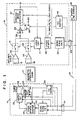
- the surveillance system includes a power line activated inductive magnetic field generator or transmitter 11 having an on-off duty cycle considerably less than 50%. While generator 11 is activated into the on duty cycle portion, it derives a first AC magnetic field having a predetermined frequency, typically 60 KHz. In the preferred embodiment, the duty cycle is approximately 6.4%, achieved by having on and off duty cycle portions with durations of 1.6 and 23.4 milliseconds, respectively.
- the magnetic field derived by generator 11 is inductively coupled from tuned coils 12 and 13, located on one wall of a region to be monitored.
- Receiver 14 is selectively responsive to the magnetic field derived by generator 11.
- Receiver 14 includes untuned magnetic field responsive coils 15 and 16, mounted on a wall opposite from the wall containing coils 12 and 13.
- receiver 14 is effectively decoupled from coils 15 and 16 while coils 12 and 13 are energized.
- a second inductive magnetic field having a fixed predetermined carrier frequency but variable duration and amplitude is coupled to coils 15 and 16 and receiver 14 immediately after expiration of the on duty cycle portion of transmitter 11 when an article containing magneto-strictive card 17 passes in the region between the walls containing coils 12, 13 and 15-16.
- the second field is detected and recognized by receiver 14 as being associated with the article passing between coils 12, 13 and 15, 16.
- Card 17 is preferably manufactured in accordance with the teachings of commonly assigned U. S. Patent 4,510,489, to Anderson III, et al. Typically, card 17 is carried on an article to be detected by an interaction of components in the card and the magnetic field derived from generator 11 and transduced by receiver 14. Card 17 is normally in an activated state, wherein it effectively functions as a resistance-inductance-capacitance (RLC) circuit that responds to the AC inductive magnetic field derived by generator 11. Card 17 stores the magnetic field derived from generator 11. When a pulse of the first magnetic field has terminated, the elements in magneto-strictive card 17 re-radiate the second magnetic field that is detected by receiver 14. Magneto-strictive card 17 is selectively deactivated by an appropriate operator, such as a checkout cashier, causing the AC inductive magnetic field re-radiated by the card to be undetectable by receiver 14.
- RLC resistance-inductance-capacitance
- Transmitter 11 and receiver 14 are synchronously activated in response to zero crossings of AC power line source 18, to enable the receiver to respond to the inductive magnetic field re-radiated from card 17 upon completion of an on duty cycle portion of transmitter 11.
- electronic circuits included in the generator and receiver need not be electrically connected together, except by power line 19 that is connected to conventional male plugs 21 and 22 of the generator and receiver, respectively.
- Generator 11 includes transmitter circuits 23 and 30 for separately and simultaneously driving tuned coils 12 and 13 with a 60 KHz carrier having a 6.4% duty cycle, such that coils 12 and 13 are supplied with sinusoidal currents at a predetermined constant frequency of 60 KHz for 1.6 milliseconds. For the next 23.4 milliseconds, coils 12 and 13 are not driven by transmitter circuits 23 and 30.
- Transmitter circuits 23 and 30 are identical, with each including a transformerless AC power line to DC converter and switch means that supplies currents from opposite terminals of the AC to DC converter to coils 12 and 13 at the 60 KHz frequency, during the on duty cycle portions.
- transmitter circuits 23 and 30 are directly responsive to the AC power line voltages on line 19, as coupled to generator 14 by way of male plug 21.
- Transmitter circuits 23 and 30 are activated into the on duty cycle portions thereof in synchronism with zero crossings of the AC voltage of power line 19, as coupled to generator 11 by way of plug 21, a result achieved by connecting zero crossing detector 24 to plug 21 so the detector derives a pulse each time the voltage on power line 19 goes through a zero value.
- the zero crossing indicating pulses derived by detector 24 are coupled to frequency synthesizer and shaper 25, having outputs fed to transmitter circuits 23 and 30, to cause the transmitter circuits to be activated to produce the 60 KHz bursts having the 6.4% duty cycle.
- DC power is supplied to components in zero crossing detector 24 and frequency synthesizer and shaper 25 by DC supply 26, connected to line 19 by male plug 21.
- Supply 26 does not have the capability of providing sufficient power to derive the necessary AC inductive magnetic fields from coils 12 and 13 to be a power supply for transmitter circuits 23 and 30.
- Transmitter circuits 23 and 30 are responsive to frequency synthesizer and shaper 25 so that both the transmitter circuits are simultaneously activated to simultaneously derive the same frequency during the on duty cycle portion of each activation cycle of the transmitter circuits.
- transmitter circuits 23 and 30 supply in phase and out of phase currents to coils 12 and 13.
- the currents supplied by transmitter circuits 23 and 30 to coils 12 and 13 cause current to flow in the same direction through the coils, relative to a common terminal for the coils.
- the currents supplied by transmitter circuits 23 and 30 to coils 12 and 13 flow in opposite directions in the coils relative to the common coil terminal.
- the switches of transmitter circuit 30 are driven during a first duty cycle portion in the same sequence as the switches of transmitter circuit 23, but during the next duty cycle portion, the activation times of the switches in transmitter circuit 30 are reversed relative to the activation times of the ransmitter circuit 30 during the preceding burst.
- phase magnetic field flux lines i.e., flux lines that are directed in the same direction in the centers of the loops
- a horizontally directed field at right angles to the plane of the loops is produced in the vicinity of adjacent wires of the loops forming coils 12 and 13.
- the magnetic flux lines between the centers of the loops forming coils 12 and 13, on one side of the plane of the loops, are oppositely directed in the vertical direction on opposite sides of adjacent wires of the loops forming coils 12 and 13.
- a vertically directed magnetic flux field in the region between tuned transmitter coils 12 and 13 and untuned coils 15 and 16 is provided by driving the loops forming coils 12 and 13 so the magnetic fluxes generated in the centers of the loop flow in opposite directions, i.e., have an out of phase relationship.
- the out of phase relationship for the fluxes of loops 12 and 13 causes the lines of flux to flow in opposite directions and cancel in the vicinity of adjacent, horizontally disposed conductor segments of the loops forming coils 12 and 13.
- the magnetic flux lines between the centers of the loops forming coils 12 and 13, on one side of the plane of the loops, are directed in the same vertical direction to cause the coils to be effectively a single coil.
- the vertically directed fluxes provide Z axis coverage for the magnetic field responsive elements in card 17.
- the fringing fields resulting from the in phase and out of phase activation of the loops forming coils 12 and 13 provide magnetic flux vectors in the Y axis, i.e., in horizontal planes parallel to the planes containing the loops of tuned transmitter coils 12 and 13 and untuned receiver coils 15 and 16.
- magnetic flux fields in three mutually orthogonal directions are derived from the loops forming coils 12 and 13 by virtue of the in phase and out of phase drives for these coils during different on duty cycle portions of transmitter circuits 23 and 30.
- These mutually orthogonal magnetic flux vectors provide coupling to enabled magneto-strictive card 17, regardless of the orientation of the card relative to the plane containing planar coils 12 and 13.
- untuned coils 15 and 16 When an activated magneto-strictive card 17 is in the region between tuned coils 12, 13 and untuned coils 15, 16 at least one of the untuned coils derives an electric signal that is a replica of the AC magnetic field derived from card 17. Because untuned coils 15 and 16 have different non-overiap- ping spatial positions and coverage areas relative to each other, and card 17, as well as coils 12 and 13, there is a fairly high likelihood of the electric signals transduced by coils 15 and 16 differing from each other.
- Receiver 14 determines if either of coils 15 or 16 is transducing a signal having the predetermined frequency, time duration and threshold amplitude necessary to signal the presence of an activated card in the region between coils 12, 13 and coils 15, 16.
- the voltages generated by coils 15 and 16 are sequentially coupled to the examining or detecting circuitry of receiver 14 during activation times synchronized with each 1.6 millisecond, 60 KHz on duty cycle burst from generator 11. After a first burst one of coils 15 or 16 is effectively coupled to the remainder of receiver 14; after the following burst the other one of coils 15 or 16 is effectively coupled to the remainder of the receiver.
- coils 15 and 16 In response to one of coils 15 and 16 generating a voltage having the required frequency, duration and amplitude values, the sequential coupling of the coils 15 and 16 to the remainder of receiver 14 is terminated. Coils 15 and 16 are activated in such a situation so that the coil which generated the voltage having the desired frequency, duration and amplitude is the only coil coupled to the remainder of receiver 14, until that coil is no longer receiving a burst having the required frequency, duration and amplitude characteristics. Thereafter, coils 15 and 16 are sequentially and altemately coupled immediately after different bursts from generator 11 to the remaining circuitry of receiver 14.
- the voltages transduced by untuned coils 15 and 16 are respectively coupled to normally open circuited switches 31 and 32 by way of preamplifiers 33 and 34.
- switches 31 or 32 During normal operation when no magnetic field having the desired characteristics is coupled to either of coils 15 or 16 in response to a burst from generator 11, one of switches 31 or 32 is closed for 25 milliseconds simultaneously with the beginning of a 1.6 millisecond burst from generator 11. Simultaneously with the next burst, the other one of switches 31 or 32 is closed for 25 milliseconds.
- Switches 31 and 32 have a common, normally open circuited terminal connected to an input terminal of automatic gain controlled amplifier 35 by way of series capacitor 36, which enables only AC levels coupled through switches 31 and 32 to be fed to the input of amplifier 35.
- the gain of amplifier 35 is preset to a predetermined level so that in response to a voltage above a threshold value being induced in one of coils 15 and 16 and coupled to the input of amplifier 35, the amplifier derives a predetermined constant amplitude output having the same frequency as the magnetic field incident on the coil. In response to the input of amplifier 35 being below a threshold level, the amplifier effectively derives a zero level.
- Synchronous detector 37 responds to the AC bursts at the output of amplifier 35 which are above the threshold value to determine if these bursts have a carrier frequency equal to the frequency of the AC magnetic field derived from an activated magneto-strictive card 17. In addition, detector 37 determines the duration of bursts having the required carrier frequency. In response to a burst having the required carrier frequency and duration, synchronous detector 37 derives a binary one level which signals that an article containing an activated magneto-strictive card 17 is in the region between tuned coils 12, 13 and untuned coils 15, 16.
- the detector is enabled by an output of frequency synthesizer 38.
- Synthesizer 38 responds to and is clocked by output pulses of zero crossing detector 39.
- the output pulses of detector 39 are synchronized with zero crossings of the AC voltage coupled by power line 19 to male plug 22.
- zero crossing detector 39 has an input connected to male plug 22, and an output on which a pulse is derived each time a zero crossing of the power line occurs.
- the pulse output of zero crossing detector 39 is applied to an input of frequency synthesizer 38.
- logic circuit 41 includes first and second inputs respectively responsive to the output of synchronous detector 37 and frequency synthesizer 38.
- synchronous detector 37 derives a binary zero output level to indicate that no activated card is between coils 12, 13 and 15, 16
- logic circuit 41 responds to frequency synthesizer 38 so that immediately after first and second successive magnetic field bursts from generator 11, switches 31 and 32 are alternately activated to the closed state.
- logic circuit 41 causes switch 31 to be activated to the closed state, while maintaining switch 32 in the open state.
- switches 31 and 32 This state of switches 31 and 32 is maintained until synchronous detector 37 again derives a binary zero level. If synchronous detector 37 derives a binary one level while switch 32 is closed, logic circuit 41 activates switches 31 and 32 so that these switches are respectively maintained in the open and closed states until a binary zero level is again derived by the synchronous detector.
- Untuned coils 15 and 16 are effectively decoupled from the remainder of receiver 14 while magnetic fluxes are being derived from coils 12 and 13 because synchronous detector 37 is effectively disabled while magnetic field bursts are derived from coils 12 and 13.
- Detector 37 in fact, is enabled by an output of synthesizer 30 only for a predetermined interval immediately after expiration of each on duty cycle portion of transmitter circuits 23 and 30.
- frequency synthesizer 38 causes the gain of amplifier 35 to be reduced to zero, causing a zero output voltage to be coupled by the amplifier to detector 37.
- synthesizer 38 includes an output that is coupled as a control input to switch 43 which is normally activated to couple the output of amplifier 35 back to a gain control input of the amplifier.
- switch 43 in response to the binary one output of frequency synthesizer 38 being coupled to the control input of switch 43, as occurs during the on duty cycle portions of transmitter circuits 23 and 30, switch 43 is activated to couple a negative DC voltage to a bias input of amplifier 35, to drive the amplifier gain to zero.
- Frequency synthesizer 38 controls synchronous detector 37 so that integrators in the detector are reset to zero during the on duty cycle portions of transmitter circuits 23 and 30.
- DC operating power is supplied to amplifiers 33-35, synchronous detector 37, frequency synthesizer 38, zero crossing detector 39 and logic circuit 41 by DC power supply 42, connected to power line 19 by way of male plug 22.
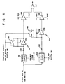
- Fig. 2 a circuit diagram of the circuitry included in transmitter circuits 23 and 30. Because the circuitry in circuits 23 and 30 is identical, the description of Fig. 2 for transmitter circuit 23 suffices for both of circuits 23 and 30.
- Transmitter circuit 23 includes a transformerless AC power line to DC power supply 51, shaping circuit 52 responsive to an output of frequency synthesizer and shaper 25, switch means 53, and resonant circuit 54 that includes coil 12.
- Shaper 52 responds to the output of frequency synthesizer and shaper 25 to supply switch means 53 with out of phase control signals.
- Switch means 53 is energized by opposite polarity voltages from transformerless power supply 51 to cause a low duty cycle current to flow in series resonant circuit 54 at the frequency supplied to the switch means by shaper 52.
- Transformerless AC power line to DC supply 51 includes full wave bridge rectifier 55, consisting of diodes 56-59, connected directly to power line leads 61 and 62.
- Diodes 56 and 57 include anodes respectively connected to leads 61 and 62, while diodes 58 and 59 include cathodes respectively connected to leads 61 and 62.
- Diodes 56 and 57 include cathodes having a common connection to electrode 63 of energy storing filter capacitor 64, while diodes 58 and 59 include anodes having a common connection to a negatively biased electrode 65 of capacitor 66.
- Electrodes 67 and 68 of capacitors 64 and 66 have a common connection at tap 69 of power supply 51. Positive and negative DC voltages are respectively derived at output terminals 71 and 72 of power supply 51, respectively connected to electrodes 63 and 65.
- Switch means 53 includes NPN bi-polar transistors 74 and 75, respectively having bases driven by out of phase control voltages from shaper 52.
- Transistors 74 and 75 include collector emitter paths that are forward biased in response to the voltages supplied to the bases thereof by shaper 52 and which are supplied with positive and negative voltages by terminals 71 and 72 of power supply 51.
- the collectors and emitters of transistors 74 and 75 are respectively connected to terminals 71 and 72, while the emitter of transistor 74 and the collector of transistor 75 have a common terminal 76.
- the emitter collector paths of transistor 74 and 75 are respectively shunted by diodes 77 and 78, poled so that current flows in them in a direction opposite from the direction of current flow in the respective shunted collector emitter path.
- Tap 69 and common terminal 76 are connected to opposite terminals of series resonant circuit 54, including inductive magnetic field transmitting coil 12, tuning capacitor 81 and resistor 82.
- the value of capacitor 81 is selected so that circuit 54 is resonant to approximately the same frequency as the switching frequency of transistors 74 and 75 during the on duty cycle portions.
- the resonant frequency of circuit 54 is rarely, if ever, exactly equal to the activation frequency of transistors 74 and 75 during the on duty cycle portion.
- Resistor 82 which controls the Q of the resonant circuit, helps to assure that sinusoidal currents having very low distortion flow in circuit 54 despite the slight deviations in the resonant frequency of circuit 54 in different generator units relative to the drive frequency of switches 74 and 75 during the on duty cycle portion.
- Transistors 74 and 75 are respectively forward biased during the positive portions of the waves illustrated in Figs. 3A and 3B. At all other times, transistors 74 and 75 are back biased. While transistor 74 is forward biased, current flows from electrode 63 of capacitor 64 through terminals 71 and the collector emitter path of transistor 74 to common terminal 76, thence through series resonant circuit 54 to tap 69 and back to the negative electrode of capacitor 64. In response to the collector emitter path of transistor 75 being forward biased, current flows from positive electrode 68 of capacitor 66 through tap 69 to series resonant circuit 54 and the collector emitter path of transistor 75 back to electrode 65 of capacitor 66 by way of terminal 72. Thus, current flows in opposite directions through series resonant circuit 54 during the complementary conduction intervals of transistors 74 and 75.
- Diodes 78 and 79 combine with resistor 82 to enable virtually distortion free sinusoidal current to flow in coil 12, even though the resonant frequency of circuit 54 differs slightly from the drive frequency for the bases of transistors 74 and 75. Because of the energy storage characteristics of coil 12 and capacitor 81, there is a tendency for current to continue to flow in resonant circuit 54 after back biasing of transistors 74 and 75. The dead time between the beginning of back biasing of one of these transistors and the forward biasing of the other transistor enables diodes 78 and 79 shunting the transistor emitter collector paths to absorb the current which has a tendency to continue to flow in resonant circuit 54.
- the voltage between tap 69 and common terminal 76 has the waveform illustrated in Fig. 3C.
- This waveform consists of positive and negative levels respectively equal to the voltages at terminals 71 and 72.
- Between the positive and negative levels of the waveform of Fig. 3C subsist zero voltage levels coincident with the dead times of transistors 74 and 75.
- the resulting voltage between tap 69 and terminal 76 is illustrated in Fig. 3E and results from the continuous current flow thru the resonant circuit 54 during the dead time of transistors 74 and 75, via the conduction paths supplied by diodes 78 and 79.
- the resultant output voltage across the resonant circuit 54 is without deadtime by virtue of the alternate conduction thru diodes 78 and 79 of the current thru the resonant circuit 54.
- a positive current having a near zero value flows in circuit 54 from terminal 76 towards tap 69 at the time transistor 74 is initially back biased. This current flows through tap 69 into electrode 68 of capacitor 66, through the capacitor and back to common terminal 76 by way of diode 79.
- the current in resonant circuit 54 changes polarity during the dead time interval, positive current flows from resonant circuit 54 to terminal 76 and diode 78 to electrode 63 of capacitor 64.
- the rectified DC voltage supplied to terminals 71 and 72 by diode bridge rectifier 75 causes capacitors 64 and 66 to be recharged.
- resistor 82 is selected so that the Q of tuned resonant circuit 54 is at least equal to eight to assist in providing the desired low distortion sinusoidal current.
- the peak amplitude of the sinusoidal current flowing in resonant circuit 54 is determined to a large extent by the resistance of resistor 82, and is approximately equal to the peak amplitude of the output voltage of inverter 51, between terminals 71 and 72, divided by the resistance of resistor 82.
- the frequency of current flowing in series resonant 54 is determined by the 60 KHz operating frequency of transistors 74 and 75, even if there is a deviation in the resonant frequency of circuit 54 from the operating frequency of the transistors. In such a situation, diodes 78 and 79 conduct the leading and lagging currents which respectively flow in resonant circuit 54 in response to the activation of frequency of transistors 74 and 75 being respectively less than and greater than the resonant frequency of circuit 54.
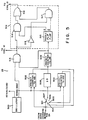
- synchronous detector 37 is illustrated as including synchronous demodulators 151 and 152, driven in parallel by the output of AGC amplifier 35.
- the output of amplifier 35, at the inputs of demodulators 151 and 152 can be assumed to be a constant amplitude sinusoid, except while coils 12 and 13 are excited during the on-duty cycle portion of generator 11.
- the sinusoidal inputs to demodulators 151 and 152 subsist for the entire off-duty cycle portion of transmitter 11.
- the sinusoidal inputs to demodulators 151 and 152 are damped sinusoids having a finite value during only a portion of the off-duty cycle portions of transmitter 11.
- the inputs to demodulators 151 and 152 drop to zero, because of the characteristics of amplifier 35.
- the output amplitude of amplifier 35 is constant.
- the length of the constant amplitude sinusoidal output of amplifier 35 during each off-duty cycle portion of generator 11 is variable, as a function of the orientation of card 17 relative to tuned transmitter coils 12, 13 and untuned receiver coils 15, 16, as well as the location of the card in the region between the coils.
- the number of cycles of the carrier frequency ⁇ i from a typical enabled card in the region is sufficient to cause accurate detection of the card.
- Synchronous detectors 151 and 152 are driven by orthogonal components of a reference wave, assumed to have a reference phase.
- the second inputs of synchronous demodulators 151, 152 can be respectively represented by:
- Synchronous demodulator 151 responds to the sin( ⁇ i t + ⁇ ) and sin ⁇ R t inputs thereof to derive an output represented by:
- synchronous demodulator 152 multiplies the two input signals thereof to derive an output signal represented by:
- the output signals of synchronous demodulators 151 and 152 are bipolarity signals that vary between plus and minus reference values, dependent upon the relative values of ⁇ i , ⁇ and ⁇ R. In response to ⁇ i and ⁇ R being equal, the outputs of demodulators 151 and 152 are DC voltages.
- demodulators 151 and 152 derive AC signals at the sum and difference frequencies ( ⁇ i + ⁇ R ) and ( ⁇ i - ⁇ R ).
- the indicated responses at the output of demodulators 151 and 152 are considered only for the difference or beat frequency ( ⁇ i - ⁇ R ). No consideration of the sum frequency ( ⁇ i + ⁇ R ) is necessary because the integration performed by detector 37 reduces these high frequency components to insignificant levels.
- Integrators 153 and 154 are standard integrators including high gain DC operational amplifiers 155 and 156, feedback capacitors 157 and 158, as well as input resistors 159 and 160. Integrators 153 and 154 are reset to zero, except during a sampling window having a duration T, during which the integrators are effectively responsive to output signals of demodulators 151 and 152. To this end, capacitors 157 and 158 are shortcircuited by switches 162 and 163 which shunt them, except during the sampling window, which begins almost immediately after the expiration of each on-duty cycle portion of transmitter 11.
- Switches 162 and 163 are simultaneously driven into the closed and open states by an output of synthesizer 30.
- the duration of sampling window T depends on the desired bandpass of synchronous detector 37, as described infra.
- the sampling window begins simultaneously with the AGC amplifier 37 being switched into an operative condition by switch 43 being coupled between the output of the amplifier and the bias input thereof.
- Comparators 165 and 166 normally derive binary zero level outputs. However, in response to the absolute value of the inputs of comparators 165 and 166 exceeding a reference value, V REF , the comparators derive binary one output levels. The binary one output levels of comparators 165 and 166 are combined in OR gate 167. A binary one level is thus derived from OR gate 167 in response to the absolute value of the integrated response over the sampling window exceeding reference value V REF . Comparators 165 and 166 derive the stated outputs in response to DC reference levels + V REF and -V REf being supplied thereto by DC supply 42.
- Signal integrators 153 and 154 derive output voltages which linearly increase with time in response to DC outputs of synchronous demodulators 151 and 152 in accordance with: and For the case where frequency ⁇ i is the same as reference frequency « R , as subsists when enabled card 17 is in the region between the transmitter and receiver coils, the output signals of integrators 153 and 154 at the completion of the sampling window, and prior to closure of switches 162 and 163, are respectively represented by cos ⁇ and sin ⁇ .
- the amplitudes at the outputs of integrators 153 and 154 are solely proportional to the duration of receiver sampling window T and the relative phase angle ⁇ between the signal coupled in parallel to demodulators 151 and 152 and the reference phase for ⁇ R.
- V, and V2 are bi-polarity voltages, having an amplitude indicative of ⁇ . This is why it is necessary to compare the absolute values of the outputs of integrators 153 and 154 with the reference level V RF .
- the duration of window T determines the effective bandpass of synchronous detector 37. If window T is long enough, any frequency ⁇ i which differs from ⁇ R will not be detected. This is because the beat frequencies derived by demodulators 151 and 152 ultimately are averaged by integrators 153 and 154 to a zero level. For the case of ⁇ i not equal to ⁇ R , the output voltages of integrators 153 and 154, at the completion of sampling window T are represented by: and Thus, integrators 153 and 154 respond to the beat frequencies, ( ⁇ i - ⁇ R ), derived from demodulators 151 and 152. Integrators 153 and 154 average the sum frequencies, ( ⁇ i , + ⁇ R ), to insignificant levels, whereby the sum frequencies have no effect on the values of V, and V Z .
- the band width ( ⁇ i - ⁇ R ) or ( ⁇ R - ⁇ i ) is determined by using the actual values for time T and the input amplitude level and transfer functions of integrators 153 and 154 to calculate the magnitudes of V, and V z .
- the synchronous demodulator-integration process achieved by demodulators 151 and 152 and integrators 153 and 154 thus has a narow frequency bandpass for long term sinusoidal signals, without including any tuned components.
- the demodulation-integration process is immune to impulse type noise, even though an impulse contains energy at all frequencies, including ⁇ R .
- the energy at any particular frequency, including ⁇ R has a short duration which prevents the output signals of integrators 153 and 154 from having an absolute value in excess of reference value V REF .
- receiver 14 is capable of discriminating an input signal having a frequency ⁇ R, with a variable unpredictable phase, and predetermined time position in the presence of background energy, as subsists in impulse type noise. This is because of the synchronous detection process provided by synchronous demodulators 151 and 152 and the time duration detecting process involving signal integrators 153 and 154.
- Synthesizer 25 responds to the pulses derived from zero crossing detector 24 to control energization of transmit circuits 23 and 30.
- Synthesizer 25 includes provision for compensating for the 120° and 240° phase displacement that is likely to subsist between the voltages at plugs 21 and 22.
- the compensation causes receiver 14 to be enabled immediately after expiration of the on-duty cycle portions of transmitter 11.
- An installer of the system of the invention merely must set one switch in each of transmitter 11 and receiver 14 to appropriate positions to provide the desired compensation.
- the installer determines which switch positions are necessary by either measuring the relative phases at the outlets connected to plugs 21 and 22 or activates generator 11 with the switches of the generator and receiver 14 in the three possible positions thereof to determine when a correct response is produced by the receiver while card 17 is in the region between tuned transmitter coils 12, 13 and untuned receiver coils 15, 16.
- the 120 Hz output signal of zero crossing detector 24 is supplied in parallel to contact 501, as well as to an enable input of each of preset counters 502 and 503.
- the preset counts of counters 502 and 503 are respectively 166 and 333.
- Counters 502 and 503 have count inputs driven by the 60 KHz output of oscillator 500. Pulses are respectively derived at the outputs of counters 502 and 503 at intervals that are respectively delayed from or displaced by 2.77 and 5.55 milliseconds from each zero crossing output pulse of detector 24; these intervals are respectively equal to 120° and 240° of the 60 Hz power line frequency at plug 21.
- the counters count the 60 KHz output of oscillator 500 up to the preset counts thereof.
- operation of the particular counter ceases until that particular counter receives another zero crossing pulse from detector 24.
- the preset counts of counters 502 and 503 the counters derive short duration pulses that are coupled to contacts 504 and 505.
- the output pulses of counters 502 and 503 are respectively applied to contacts 504 and 505 of manually controlled three-position switch 506, including armature 507.
- Armature 507 is positioned to engage terminals or contacts 501, 504 and 505 when the single phase 60 Hz voltages at plugs 21 and 22 in phase, 120° displaced and 240° displaced, respectively.
- Armature 507 of switch 506 is permanently connected to divide by three frequency divider 508, which derives a 40 Hz pulse output train.
- the 40 Hz pulse train determines the frequency of the inductive magnetic fields derived from coils 12 and 13 (but not the carrier frequency).
- the magnetic fields are derived from coils 12 and 13 at a frequency that is anharmonically related to 60 Hz to assist in providing a secure system that is immune to persons who use devious means to desensitize the system.
- Such persons would normally think that the 60 KHz bursts are derived at a frequency of 60 Hz or a harmonic of 60 Hz.
- a burst occurrence frequency that is anharmonically related to 60 Hz such desensitizing or jamming can be reduced.
- the 40 Hz output of frequency divider 508 is coupled to preset counter 509 that responds to the pulses on armature 507 and to the 60 KHz output of oscillator 500 in a manner similar to the manner in which counters 502 and 503 operate.
- the count of counter 509 is preset to a value of 96, to provide the 1.6 millisecond on-duty cycle duration for transmitter 11. For the entire time that counter 509 is counting up to 96, it derives a binary one output level which is coupled to an enable input of AND gate 513, causing the gate to pass the 60 KHz output of oscillator 500.
- 96 cycles of the 60 KHz output of oscillator 500 are passed through AND gate 513 while counter 509 is counting to its preset value of 96.
- the 60 KHz output of AND gate 513 is applied to shaper 42 of transmit circuit 23.
- Shaper 42 responds to the 60 KHz oscillations to provide the dead times discussed supra.
- Ninety-six cycles of 60 KHz current are thereby supplied to coil 12 for 1.6 milliseconds every 25 milliseconds, at a time position synchronized by the zero crossings of the power line connected to plug 21.
- Circuit 514 Inverts the 60 KHz output of oscillator 500 during alternate on-duty cycle durations of transmit circuit 30, to enable alternate in- phase and out-of-phase AC inductive magnetic fields to be derived.
- Circuit 514 includes toggle flip-flop 515 responsive to the trailing edge output of counter 509. Toggle flip-flop 515 includes complementary Q and 1r outputs, having a frequency one-half that of the output of counter 509; transitions in the Q and 7 7 outputs are synchronized with the expiration of each magnetic field derived from transmitter 11.
- the Q and Q outputs of flip-flop 515 are respectively applied to enable inputs of AND gates 516 and 517, respectively driven by uninverted and inverted replicas of the 60 KHz output of AND gate 513; inverter 519 is connected between the output of AND gate 513 and an input of AND gate 517 to provide the inversion.
- the outputs of AND gates 516 and 517 are coupled to OR gate 518, which drives coil 13.
- AND gate 516 is enabled to pass the uninverted 60 KHz output of AND gate 513 to OR gate 518.
- the ZF output of flip-flop 515 enables AND gate 517 to pass the inverted 60 KHz output of inverter 519 to coil 13 by way of OR gate 518.
- Synthesizer 38 causes receiver 14 to be enabled at a frequency that is three times greater than the 40 Hz activation frequency of transmitter or generator 11. Enabling receiver 14 at a frequency that is an integral multiple of the operating frequency of generator 11 assists in making the system more difficult to jam and enables a single receiver to be responsive to multiple transmitters in the same vicinity.
- Receiver 14 is synchronized so that it can be responsive to multiple transmitters, powered by phase displaced AC power line voltages.
- Synthesizer 38 includes free running 60 KHz oscillator 531, having output leads 532 and 533 on which are derived 60 KHz waves that are phase displaced from each other by 90° and, thereby, can be respectively considered as sine and cosine waves.
- the sine and cosine waves on leads 532 and 533 are respectively applied to synchronous demodulators 151 and 152 in synchronous detector 37.
- the sine wave on lead 532 is also used to establish 1.6 millisecond wide receiver sampling windows, which subsist in receiver 14 immediately after expiration of each possible 1.6 millisecond, 60 KHz burst of each of generators 11, following a zero crossing at the power line input of the generator.
- receiver 14 is, in the preferred embodiment, enabled three times during each 40 Hz operating cycle of generator or transmitter 11. These three enablement times are synchronized with the three possible time positions of the 40 Hz on duty cycle portions of the 60 KHz wave derived by transmitter 11. Compensation is made for the phase of the power line voltage at plug 22 of receiver 14.
- the 120 Hz output pulse waveform of zero crossing detector 39 is applied to terminal 535 of three-position switch 536, including contacts 537-539, and armature 540.
- Armature 540 engages contacts 537, 538 and 539 to provide 0°, 60° and 120° phase delay for the possible 0°, 120° and 240° phase displacement of the AC power line voltage at plug 22 relative to the power line voltage at plug 21.
- the pulse waveform at terminal 535 is applied in parallel to enable inputs of preset counters 542 and 543, having count inputs driven in parallel by the 60 KHz sine wave on lead 532.
- Counters 542 and 543 are respectively preset to counts of 166 and 332 to provide time delays of 2.77 and 5.55 milliseconds.
- the output pulses of counters 542 and 543 are thereby phase displaced by 60° and 120° relative to the 60 Hz zero crossings at plug 22.
- Contact 540 is adjusted to engage contacts 537, 538 and 539, so that pulses on the contact are either in phase with zero crossings at plug 22, are phase displaced by 60° with the 60 Hz zero crossings at plug 22, or are phase displaced by 120° with the zero crossings at plug 22.
- the pulses on contact 540 are applied to an enable input of preset counter 544, having a count input responsive to the 60 KHz wave on lead 532.
- Counter 544 is preset to a count of 96, thereby to derive a trailing edge that is time displaced by 1.6 milliseconds from the pulses on contact 540.
- the trailing edge of the output of counter 544 occurs simultaneously with each possible expiration of a 60 KHz burst from transmitter 11.
- the trailing edge of the output of preset counter 544 initiates an enable cycle of receiver 14.
- the trailing edge output of preset counter 544 is supplied to an enable input of preset counter 545, having a count input responsive to the 60 KHz wave on lead 532.
- Counter 545 is preset to a count of 96, to establish a 1.6 millisecond receiver sampling window. During the 1.6 milliseconds while counter 545 is counting the 60 KHz wave on lead 532 to a count of 96, the counter derives a binary one output level. During the interval while counter 545 derives a binary one output level, AGC switch 43 and capacitor discharge switches 162 and 163 are activated so that the receiver is effectively enabled.
- switches 162 and 163 are open circuited, while switch 43 is energized to establish the AGC feedback path for amplifier 35, such that the amplifier is not cutoff by the negative DC bias voltage applied to switch 43. If the output of OR gate 167 is sufficiently great during this interval, a binary one level is derived by OR gate 167 to indicate the presence of an activated card in the surveillance region.
- receiver 14 is enabled at a frequency which is three times that of the 60 KHz output bursts of generator 11, and the possibility of more than one generator being in a region to which receiver 14 is responsive, and the different, altemate phases of the inductive fields that are derived by one transmitter or generator 11, it is necessary for untuned receiver coils 15 and 16 to stay in the same condition for six successive enablement cycles of the receiver.
- switch 31 is closed while switch 32 is open during six successive enablement cycles of receiver 14, and vice versa. Switches 31 and 32 must be switched between the open and closed states in synchronism with the remainder of receiver 14 being enabled.
- the 120 Hz, phase synchronized pulse waveform on armature 540 is coupled to an input of divide by twelve frequency divider 546.
- Frequency divider 546 has complementary Q and %x outputs on leads 547 and 548.
- the complementary binary signals on leads 547 and 548 are applied as control inputs to switches 31 and 32, respectively.
- switches 31 and 32 are respectively closed and opened. Because of the divide by twelve factor of divider 546, switch 31 remains closed for six enablement cycles of receiver 14, followed by switch 32 being closed for six successive enablement cycles of the receiver.
- logic circuit 41 As illustrated in Fig. 7, is included. Basically, logic circuit 41 responds to frequency synthesizer 38 to alternately close switches 31 and 32 during different successive detection cycles of receiver 14, which occur Immediately after successive, different alternate on duty cycle portions of coils 12 and 13. In response to one of coils 15 or 16 causing detector 37 to derive an output indicative of the presence of card 17 in surveillance zone 201, logic circuit 41 maintains the switch which was closed in a closed condition.
- logic circuit 41 includes AND gate 231 having a first input responsive to an output of frequency synthesizer 38 at the 40 Hz activation frequency of the on duty cycle portions of generator 11.
- Frequency synthesizer 38 supplies gate 231 with a short duration binary one level coincident with the start time of each on duty cycle portion of transmitter circuits 23 and 30.
- Gate 231 is normally enabled to pass the output of frequency synthesizer 39 to a clock input terminal of toggle or D flip-flop 232, having complementary Q and -a outputs which respectively control opening and closing of switches 31 and 32.
- switch 31 is respectively closed and opened.
- binary one and zero states for the Q output of flip-flop 232 result in switch 32 being closed and opened.
- Pulses from frequency synthesizer 38 are inhibited by AND gate 231 in response to synchronous detector 37 detecting a 60 KHz reponse from card 17.
- the output of synthesizer 38 is coupled to delay network and pulse shaper circuit 233.
- Circuit 233 derives a short duration output pulse that is delayed relative to the input of gate 231 from synthesizer 38 by a sufficient time to enable derivation by detector 37 of a binary one signal indicating the presence of magneto-strictive card 17.
- This pulse output of circuit 233 is applied to AND gate 234.
- the output of gate 234 is applied to the set input of set-reset flip-flop 235.
- Delay and pulse shaper circuit 233 also generates a second output in the form of a short duration pulse coincident with the termination of the on duty cycle portion of transmitter circuits 23 and 30. This second output is applied to the reset input of set-reset flip-flop 235.
- gate 234 In response to detector 37 deriving a binary one output to indicate the presence of card 17, gate 234 is enabled to cause the T3 output of flip-flop 235 to be set to the zero state.
- AND gate 234 In contrast, in response to detector 37 deriving a binary zero output while a pulse is derived from circuit 233, AND gate 234 remains in its binary zero state hence the Q output of flip flop 235 remains in a binary one state initiated by the reset pulse output of circuit 233.
Abstract
Description
- The present invention relates generally to article surveillance systems and more particularly to an article surveillance system including a power line activated transmitter and a power line activated receiver wherein the transmitter and receiver are synchronized by zero crossings of the power lines energizing them.
- An article surveillance system has been developed wherein a transmitter or generator periodically derives a first inductive magnetic field having a carrier frequency. The first magnetic field is coupled to a structure on a surveilled article. The structure resembles a tuned or resistance-inductance-capacitance (RLC) circuit. Upon completion of the first magnetic field, the structure radiates a second magnetic field having a frequency that is equal to or approximately equal to the frequency of the first field. A receiver for the second magnetic field is activated in synchronism with the derivation of the second magnetic field. Preferably, the receiver is effectively disabled while the first magnetic field is being derived so that the first magnetic field is not detected as the field associated with the structure.
- The receiver detects the occurrence of the second magnetic field for a predetermined time to indicate the presence of the surveilled article. In the preferred prior art receiver, the detection process involves synchronously demodulating a replica of the second magnetic field as incident on a pick up coil arrangement of the receiver. The length of time that a synchronous demodulator derives an output having a frequency equal to the frequency of the second magnetic field provides a measure of the length of time that the second magnetic field is incident on the coil arrangement. The length of time is determined by an integration process that is initiated immediately after expiration of the first magnetic field and has a predetermined duration determined by the band width of the detection process. While the first magnetic field is being derived, the synchronous demodulator and an integrator means are effectively decoupled from the receiver coil arrangement by reducing the gain of an amplifier between the coil and synchronous demodulator to zero. Thus, it is important to provide synchronization between the derivation of
- magnetic field pulses from the transmitter and operation of the receiver.
- In the past, synchronization between the transmitter and receiver of article surveillance systems has been usually attained by physically linking the transmitter and receiver with a hard wire cable, activated by a periodic source, e.g. an oscillator which is a part of the transmitter. The oscillator causes the transmitter to supply periodic pulses to the receiver via the hard wire cable. The use of a hard wire cable between the transmitter and receiver results in a further installation expense of the article surveillance system because of the desire to hide any wires which extend through the region where the transmitter and receiver are located. Seemingly, the need for a cable between the transmitter and receiver can be obviated by utilizing electric and/or magnetic fields to synchronize the transmitter and receiver. However, the use of such fields is beset with pitfalls, particularly because of likely interference.
- It is, accordingly, an object of the present invention to provide a new and improved article surveillance system including a synchronized transmitter and receiver.
- A further object of the invention is to provide a new and improved article surveillance system wherein synchronization of a transmitter and receiver is attained without any added wires between the transmitter and receiver, as well as without the need for electric or magnetic fields between the transmitter and receiver.
- In accordance with the present invention, an article surveillance system is provided wherein a structure responds to a first pulsed inductive magnetic field to derive a second pulsed inductive magnetic field having a predetermined occurrence time relative to the occurrence time of the first magnetic field. The system includes power line activated transmitter means for periodically deriving the first pulsed inductive magnetic field. Power line activated receiver means responds to the second pulsed inductive magnetic field. The occurrence time of the first magnetic field and the activation time of the receiver means are sychronized so that the receiver means is activated while the second magnetic field is incident on coil means of the receiver means. Synchronization is provided by first and second separate zero crossing detectors for power lines activating the transmitter means and the receiver means. The first and second zero crossing detectors are respectively included in the transmitter and receiver means.
- Most article surveillance systems are installed in facilities, such as retail store establishments, wherein a conventional single-phase power line, operating at 115 volts, 60 Hz (in the United States) is derived from a three-phase line. Because of this factor, the phases at outlets energizing the power line activated transmitter and the power line activated receiver are not necessarily the same. Frequently, the phases at the power line activated transmitter and receiver are displaced from each other by 120° or 240°. Hence, the zero crossings at the outlets energizing the transmitter and receiver are likely to be displaced from each other by 60° or 120° of the power line frequency.
- It is, accordingly, another object of the present invention to provide a new and improved article surveil lance system including a transmitter and receiver synchronized by power line zero crossings wherein compensation is provided for the likelihood of the transmitter and receiver being connected to power line outlets having different phases.
- To solve the problem of the power line outlets having different phases, at least one of the power line activated transmitter or receiver means includes means for compensating for the different predetermined time positions of the zero crossings. In the preferred embodiment, the compensating means for one of the transmitter and receiver means includes preset counter means responsive to a signal having an occurrence time controlled by the zero crossing time of the power line activating said one transmitter or receiver means. Switch means selectively controls the preset count of the counter means.
- The above and still further objects, features and advantages of the present invention will become apparent upon consideration of the following detailed description of one specific embodiment thereof, especially when taken in conjunction with the accompanying drawings.
-
- Fig. 1 is a block diagram of an article surveillance system including a magnetic field generator in accordance with the present invention;
- Fig. 2 is a circuit diagram of a transmit circuit included in Fig. 1;
- Figs 3A - 3E are waveforms useful in helping to describe the operation of Fig. 2;
- Fig. 4 is a schematic and circuit block diagram of the synchronous detector in the receiver in the system of Fig. 1;
- Fig. 5 is a block and circuit diagram of the synthesizer of the generator in Fig. 1;
- Fig. 6 is a block and circuit diagram of the synthesizer in the receiver in the system of Fig. 1; and
- Fig. 7 is a curcuit diagram of the logic circuit included in the receiver circuit of Fig. 1.
- Reference is now made to Fig. 1 of the drawing wherein there is illustrated a surveillance system incorporating the present invention. The surveillance system includes a power line activated inductive magnetic field generator or transmitter 11 having an on-off duty cycle considerably less than 50%. While generator 11 is activated into the on duty cycle portion, it derives a first AC magnetic field having a predetermined frequency, typically 60 KHz. In the preferred embodiment, the duty cycle is approximately 6.4%, achieved by having on and off duty cycle portions with durations of 1.6 and 23.4 milliseconds, respectively. The magnetic field derived by generator 11 is inductively coupled from tuned
coils - Inductive AC magnetic field power line activated
receiver 14 is selectively responsive to the magnetic field derived by generator 11.Receiver 14 includes untuned magnetic field responsive coils 15 and 16, mounted on a wall opposite from thewall containing coils coils coils receiver 14 is effectively decoupled from coils 15 and 16 whilecoils receiver 14 immediately after expiration of the on duty cycle portion of transmitter 11 when an article containing magneto-strictive card 17 passes in the region between thewalls containing coils receiver 14 as being associated with the article passing betweencoils -
Card 17 is preferably manufactured in accordance with the teachings of commonly assigned U. S. Patent 4,510,489, to Anderson III, et al. Typically,card 17 is carried on an article to be detected by an interaction of components in the card and the magnetic field derived from generator 11 and transduced byreceiver 14.Card 17 is normally in an activated state, wherein it effectively functions as a resistance-inductance-capacitance (RLC) circuit that responds to the AC inductive magnetic field derived by generator 11.Card 17 stores the magnetic field derived from generator 11. When a pulse of the first magnetic field has terminated, the elements in magneto-strictive card 17 re-radiate the second magnetic field that is detected byreceiver 14. Magneto-strictive card 17 is selectively deactivated by an appropriate operator, such as a checkout cashier, causing the AC inductive magnetic field re-radiated by the card to be undetectable byreceiver 14. - Transmitter 11 and
receiver 14 are synchronously activated in response to zero crossings of AC power line source 18, to enable the receiver to respond to the inductive magnetic field re-radiated fromcard 17 upon completion of an on duty cycle portion of transmitter 11. By synchronizing the operation of generator 11 andreceiver 14 in response to zero crossings of AC power line source 18, electronic circuits included in the generator and receiver need not be electrically connected together, except bypower line 19 that is connected to conventional male plugs 21 and 22 of the generator and receiver, respectively. - Generator 11 includes
transmitter circuits tuned coils transmitter circuits -
Transmitter circuits coils transmitter circuits line 19, as coupled togenerator 14 by way ofmale plug 21.Transmitter circuits power line 19, as coupled to generator 11 by way ofplug 21, a result achieved by connecting zerocrossing detector 24 to plug 21 so the detector derives a pulse each time the voltage onpower line 19 goes through a zero value. The zero crossing indicating pulses derived bydetector 24 are coupled to frequency synthesizer andshaper 25, having outputs fed totransmitter circuits - DC power is supplied to components in zero
crossing detector 24 and frequency synthesizer andshaper 25 by DC supply 26, connected toline 19 bymale plug 21. Supply 26 does not have the capability of providing sufficient power to derive the necessary AC inductive magnetic fields fromcoils transmitter circuits -
Transmitter circuits shaper 25 so that both the transmitter circuits are simultaneously activated to simultaneously derive the same frequency during the on duty cycle portion of each activation cycle of the transmitter circuits. During alternate on duty cycle portions,transmitter circuits coils transmitter circuits coils transmitter circuits coils - Such a result is achieved by
synthesizer 25 activating switches intransmitter circuits transmitter circuits shaper 25 to cause the AC currents incoils transmitter circuit 23 are always driven in the same sequence. In contrast, the switches oftransmitter circuit 30 are driven during a first duty cycle portion in the same sequence as the switches oftransmitter circuit 23, but during the next duty cycle portion, the activation times of the switches intransmitter circuit 30 are reversed relative to the activation times of theransmitter circuit 30 during the preceding burst. - In response to
coils circuits loops forming coils loops forming coils loops forming coils - Hence, in response to the stated in phase magnetic fluxes in the
loops forming coils card 17 but there is a weak vertical magnetic field due to the cancellation effect of the oppositely directed vertical fields. - A vertically directed magnetic flux field in the region between tuned transmitter coils 12 and 13 and untuned coils 15 and 16 is provided by driving the
loops forming coils loops loops forming coils loops forming coils card 17. - The fringing fields resulting from the in phase and out of phase activation of the
loops forming coils loops forming coils transmitter circuits strictive card 17, regardless of the orientation of the card relative to the plane containingplanar coils - When an activated magneto-
strictive card 17 is in the region betweentuned coils card 17. Because untuned coils 15 and 16 have different non-overiap- ping spatial positions and coverage areas relative to each other, andcard 17, as well as coils 12 and 13, there is a fairly high likelihood of the electric signals transduced by coils 15 and 16 differing from each other. -
Receiver 14 determines if either of coils 15 or 16 is transducing a signal having the predetermined frequency, time duration and threshold amplitude necessary to signal the presence of an activated card in the region betweencoils receiver 14 during activation times synchronized with each 1.6 millisecond, 60 KHz on duty cycle burst from generator 11. After a first burst one of coils 15 or 16 is effectively coupled to the remainder ofreceiver 14; after the following burst the other one of coils 15 or 16 is effectively coupled to the remainder of the receiver. In response to one of coils 15 and 16 generating a voltage having the required frequency, duration and amplitude values, the sequential coupling of the coils 15 and 16 to the remainder ofreceiver 14 is terminated. Coils 15 and 16 are activated in such a situation so that the coil which generated the voltage having the desired frequency, duration and amplitude is the only coil coupled to the remainder ofreceiver 14, until that coil is no longer receiving a burst having the required frequency, duration and amplitude characteristics. Thereafter, coils 15 and 16 are sequentially and altemately coupled immediately after different bursts from generator 11 to the remaining circuitry ofreceiver 14. - To these ends, the voltages transduced by untuned coils 15 and 16 are respectively coupled to normally open circuited switches 31 and 32 by way of
preamplifiers switches switches Switches amplifier 35 by way ofseries capacitor 36, which enables only AC levels coupled throughswitches amplifier 35. The gain ofamplifier 35 is preset to a predetermined level so that in response to a voltage above a threshold value being induced in one of coils 15 and 16 and coupled to the input ofamplifier 35, the amplifier derives a predetermined constant amplitude output having the same frequency as the magnetic field incident on the coil. In response to the input ofamplifier 35 being below a threshold level, the amplifier effectively derives a zero level. -
Synchronous detector 37 responds to the AC bursts at the output ofamplifier 35 which are above the threshold value to determine if these bursts have a carrier frequency equal to the frequency of the AC magnetic field derived from an activated magneto-strictive card 17. In addition,detector 37 determines the duration of bursts having the required carrier frequency. In response to a burst having the required carrier frequency and duration,synchronous detector 37 derives a binary one level which signals that an article containing an activated magneto-strictive card 17 is in the region betweentuned coils - To control the operation of
receiver 14 so thatsynchronous detector 37 is energized for the correct time interval associated with activatedcard 17 being in the region betweentuned coils frequency synthesizer 38.Synthesizer 38 responds to and is clocked by output pulses of zerocrossing detector 39. The output pulses ofdetector 39 are synchronized with zero crossings of the AC voltage coupled bypower line 19 tomale plug 22. To this end, zerocrossing detector 39 has an input connected tomale plug 22, and an output on which a pulse is derived each time a zero crossing of the power line occurs. The pulse output of zerocrossing detector 39 is applied to an input offrequency synthesizer 38. - To control the operation of
switches logic circuit 41 includes first and second inputs respectively responsive to the output ofsynchronous detector 37 andfrequency synthesizer 38. During normal operation, whensynchronous detector 37 derives a binary zero output level to indicate that no activated card is betweencoils logic circuit 41 responds tofrequency synthesizer 38 so that immediately after first and second successive magnetic field bursts from generator 11, switches 31 and 32 are alternately activated to the closed state. In repsonse to switch 31 being closed at thetime synchronous detector 37 derives a binary one level to indicate anenabled card 17 betweencoils logic circuit 41 causes switch 31 to be activated to the closed state, while maintainingswitch 32 in the open state. This state ofswitches synchronous detector 37 again derives a binary zero level. Ifsynchronous detector 37 derives a binary one level whileswitch 32 is closed,logic circuit 41 activates switches 31 and 32 so that these switches are respectively maintained in the open and closed states until a binary zero level is again derived by the synchronous detector. - Untuned coils 15 and 16 are effectively decoupled from the remainder of
receiver 14 while magnetic fluxes are being derived fromcoils synchronous detector 37 is effectively disabled while magnetic field bursts are derived fromcoils Detector 37, in fact, is enabled by an output ofsynthesizer 30 only for a predetermined interval immediately after expiration of each on duty cycle portion oftransmitter circuits transmitter circuits frequency synthesizer 38 causes the gain ofamplifier 35 to be reduced to zero, causing a zero output voltage to be coupled by the amplifier todetector 37. To this end,synthesizer 38 includes an output that is coupled as a control input to switch 43 which is normally activated to couple the output ofamplifier 35 back to a gain control input of the amplifier. However, in response to the binary one output offrequency synthesizer 38 being coupled to the control input of switch 43, as occurs during the on duty cycle portions oftransmitter circuits amplifier 35, to drive the amplifier gain to zero.Frequency synthesizer 38 controlssynchronous detector 37 so that integrators in the detector are reset to zero during the on duty cycle portions oftransmitter circuits - DC operating power is supplied to amplifiers 33-35,
synchronous detector 37,frequency synthesizer 38, zerocrossing detector 39 andlogic circuit 41 byDC power supply 42, connected topower line 19 by way ofmale plug 22. - Reference is now made to Fig. 2, a circuit diagram of the circuitry included in
transmitter circuits circuits transmitter circuit 23 suffices for both ofcircuits -
Transmitter circuit 23 includes a transformerless AC power line toDC power supply 51, shapingcircuit 52 responsive to an output of frequency synthesizer andshaper 25, switch means 53, andresonant circuit 54 that includescoil 12.Shaper 52 responds to the output of frequency synthesizer andshaper 25 to supply switch means 53 with out of phase control signals. Switch means 53 is energized by opposite polarity voltages fromtransformerless power supply 51 to cause a low duty cycle current to flow in seriesresonant circuit 54 at the frequency supplied to the switch means byshaper 52. - Transformerless AC power line to
DC supply 51 includes fullwave bridge rectifier 55, consisting of diodes 56-59, connected directly to power line leads 61 and 62.Diodes diodes Diodes electrode 63 of energy storingfilter capacitor 64, whilediodes electrode 65 ofcapacitor 66.Electrodes capacitors tap 69 ofpower supply 51. Positive and negative DC voltages are respectively derived atoutput terminals power supply 51, respectively connected toelectrodes - Switch means 53 includes NPN
bi-polar transistors shaper 52.Transistors shaper 52 and which are supplied with positive and negative voltages byterminals power supply 51. The collectors and emitters oftransistors terminals transistor 74 and the collector oftransistor 75 have acommon terminal 76. The emitter collector paths oftransistor diodes -
Tap 69 andcommon terminal 76 are connected to opposite terminals of seriesresonant circuit 54, including inductive magneticfield transmitting coil 12, tuningcapacitor 81 andresistor 82. The value ofcapacitor 81 is selected so thatcircuit 54 is resonant to approximately the same frequency as the switching frequency oftransistors coil 12 and the capacitance ofcapacitor 81, the resonant frequency ofcircuit 54 is rarely, if ever, exactly equal to the activation frequency oftransistors Resistor 82, which controls the Q of the resonant circuit, helps to assure that sinusoidal currents having very low distortion flow incircuit 54 despite the slight deviations in the resonant frequency ofcircuit 54 in different generator units relative to the drive frequency ofswitches - In operation, there is a slight dead time between the end of a forward bias interval for the collector emitter path of
transistor switch 74 and the initiation of a forward bias for the collector emitter path oftransistor 75 during each 60 KHz cycle of the drive provided for the bases oftransistors switch 75 to switch 74. The dead time is provided byshaper 52 responding to a 60 KHz input fromsynthesizer 25, to supply the bases oftransistors -
Transistors transistors transistor 74 is forward biased, current flows fromelectrode 63 ofcapacitor 64 throughterminals 71 and the collector emitter path oftransistor 74 tocommon terminal 76, thence through seriesresonant circuit 54 to tap 69 and back to the negative electrode ofcapacitor 64. In response to the collector emitter path oftransistor 75 being forward biased, current flows frompositive electrode 68 ofcapacitor 66 throughtap 69 to seriesresonant circuit 54 and the collector emitter path oftransistor 75 back toelectrode 65 ofcapacitor 66 by way ofterminal 72. Thus, current flows in opposite directions through seriesresonant circuit 54 during the complementary conduction intervals oftransistors - Because of the low duty cycle forward biasing of
transistors capacitors DC converter 51 to be employed. The maximum duty cycle for activatingswitching transistors strictive card 17,synchronous detector 37 ofreceiver 14, and the circuitry and components of AC toDC converter 51. -
Diodes 78 and 79 combine withresistor 82 to enable virtually distortion free sinusoidal current to flow incoil 12, even though the resonant frequency ofcircuit 54 differs slightly from the drive frequency for the bases oftransistors coil 12 andcapacitor 81, there is a tendency for current to continue to flow inresonant circuit 54 after back biasing oftransistors diodes 78 and 79 shunting the transistor emitter collector paths to absorb the current which has a tendency to continue to flow inresonant circuit 54. - When
transistors tap 69 andcommon terminal 76 has the waveform illustrated in Fig. 3C. This waveform consists of positive and negative levels respectively equal to the voltages atterminals transistors - In response to the voltage between
tap 69 and terminal 76 impressed acrossresonant circuit 54 with a resonant frequency equal to the activation frequency oftransistors resonant circuit 54. - The resulting voltage between
tap 69 andterminal 76 is illustrated in Fig. 3E and results from the continuous current flow thru theresonant circuit 54 during the dead time oftransistors diodes 78 and 79. - Thus even through there exists a dead time in the drive signals to
transistors resonant circuit 54 is without deadtime by virtue of the alternate conduction thrudiodes 78 and 79 of the current thru theresonant circuit 54. Typically, a positive current having a near zero value flows incircuit 54 fromterminal 76 towardstap 69 at thetime transistor 74 is initially back biased. This current flows throughtap 69 intoelectrode 68 ofcapacitor 66, through the capacitor and back tocommon terminal 76 by way of diode 79. When the current inresonant circuit 54 changes polarity during the dead time interval, positive current flows fromresonant circuit 54 toterminal 76 anddiode 78 toelectrode 63 ofcapacitor 64. - When the collector emitter path of
transistor 75 is forward biased, the current flowing from series resonant 54 continues to flow toterminal 76, but now flows through the low impedance collector emitter path oftransistor 75 throughcapacitor 66 to tap 69. Whiletransistor 75 is forward biased, current drains fromcapacitor 66 into the load provided by seriesresonant circuit 54 andtransistor 75. Thus, whiletransistor 75 is forward biased, current flows fromtap 69 toterminal 76 through seriesresonant circuit 54 in a direction opposite from the direction of current flow through the series resonant circuit whiletransistor 74 is forward biased. Whentransistor 75 is cut off, the current flowing inresonant circuit 54 throughterminal 76 is shifted so that it flows throughdiode 78 to assist in rechargingcapacitor 64. Such current flow continues during the dead time until there is a reversal in the direction of current flow inresonant circuit 54, at whichtime capacitor 66 is supplied with charging current by way of the path completed through diode 79. - During the off duty cycle portion, as subsists for more than 90% of the time with the specified on and off duty cycle durations of 1.6 end 23.4 milliseconds, respectively, the rectified DC voltage supplied to
terminals diode bridge rectifier 75causes capacitors - The value of
resistor 82 is selected so that the Q of tunedresonant circuit 54 is at least equal to eight to assist in providing the desired low distortion sinusoidal current. The peak amplitude of the sinusoidal current flowing inresonant circuit 54 is determined to a large extent by the resistance ofresistor 82, and is approximately equal to the peak amplitude of the output voltage ofinverter 51, betweenterminals resistor 82. - The frequency of current flowing in series resonant 54 is determined by the 60 KHz operating frequency of
transistors circuit 54 from the operating frequency of the transistors. In such a situation,diodes 78 and 79 conduct the leading and lagging currents which respectively flow inresonant circuit 54 in response to the activation of frequency oftransistors circuit 54. - Because of the switch-mode operation of
transmitter circuit 23, whereintransistors circuit 54'reduces stresses and switching losses oftransistors - Reference is now made to Fig. 4 of the drawing wherein
synchronous detector 37 is illustrated as includingsynchronous demodulators AGC amplifier 35. When an activated magneto-strictive card 17 is in the region between tuned transmitter coils 12, 13 and untuned receiver coils 15, 16, the output ofamplifier 35, at the inputs ofdemodulators coils demodulators amplifier 35 can be assumed to vary in accordance with:
enabled card 17 after the on-duty cycle portion of transmitter 11 has terminated,
card 17, as incident on the coil 15 or 16 feeding the remainder of the receiver. - For the purposes of this description it is assumed that the sinusoidal inputs to
demodulators demodulators demodulators amplifier 35. As long as the sinusoid is above a predetermined level, the output amplitude ofamplifier 35 is constant. The length of the constant amplitude sinusoidal output ofamplifier 35 during each off-duty cycle portion of generator 11 is variable, as a function of the orientation ofcard 17 relative to tuned transmitter coils 12, 13 and untuned receiver coils 15, 16, as well as the location of the card in the region between the coils. However, due to the detection process employed indetector 37, the number of cycles of the carrier frequency ωi, from a typical enabled card in the region is sufficient to cause accurate detection of the card. -
Synchronous detectors synchronous demodulators - sin«Rt, and
- COSωRt,
- where:
- ωR = the angular frequency of the reference wave, which in turn is equal to the frequency of the AC carrier wave derived from the structure on
card 17. -
Synchronous demodulator 151 responds to the sin(ωit + φ) and sinωRt inputs thereof to derive an output represented by:
synchronous demodulator 152 multiplies the two input signals thereof to derive an output signal represented by:
synchronous demodulators demodulators card 17,demodulators demodulators detector 37 reduces these high frequency components to insignificant levels. - The output signals of
demodulators analog signal integrators Integrators operational amplifiers feedback capacitors input resistors Integrators demodulators capacitors switches Switches synthesizer 30. The duration of sampling window T depends on the desired bandpass ofsynchronous detector 37, as described infra. The sampling window begins simultaneously with theAGC amplifier 37 being switched into an operative condition by switch 43 being coupled between the output of the amplifier and the bias input thereof. - The output levels of
integrators comparators Comparators comparators comparators gate 167. A binary one level is thus derived from ORgate 167 in response to the absolute value of the integrated response over the sampling window exceeding reference value VREF. Comparators 165 and 166 derive the stated outputs in response to DC reference levels + VREF and -VREf being supplied thereto byDC supply 42. -
Signal integrators synchronous demodulators 

card 17 is in the region between the transmitter and receiver coils, the output signals ofintegrators switches 

integrators demodulators - Because the relative phase angle 0 is unpredictably variable between 0° and 360°, voltages V, and V2 are bi-polarity voltages, having an amplitude indicative of φ. This is why it is necessary to compare the absolute values of the outputs of
integrators comparators 
integrators 153end 154. This value of V, is multiplied by cos45° (equal approximately to 0.707), resulting in 2 cos45° = 0.35T. By setting VREF = 0.35T all input signals having a frequency ωi=ωR are detected, regardless of phase since either V, or V2 is never less than 0.35T. - The duration of window T determines the effective bandpass of
synchronous detector 37. If window T is long enough, any frequency ωiwhich differs from ωR will not be detected. This is because the beat frequencies derived bydemodulators integrators integrators 

integrators demodulators Integrators - The band width of the demodulation and integration process can be determined by evaluating the two last presented equations at time t = 0 and any other time t between zero and the maximum duration that the sinusoidal voltage can be derived from
demodulators strictive card 17. The band width (ωi-ωR) or (ωR-ωi) is determined by using the actual values for time T and the input amplitude level and transfer functions ofintegrators detector 37 is equal to
- The synchronous demodulator-integration process achieved by
demodulators integrators integrators receiver 14 is capable of discriminating an input signal having a frequency ωR, with a variable unpredictable phase, and predetermined time position in the presence of background energy, as subsists in impulse type noise. This is because of the synchronous detection process provided bysynchronous demodulators signal integrators - Reference is now made to Fig. 5 of the drawing wherein details of
transmitter synthesizer 25 are illustrated.Synthesizer 25 responds to the pulses derived from zerocrossing detector 24 to control energization of transmitcircuits Synthesizer 25 includes provision for compensating for the 120° and 240° phase displacement that is likely to subsist between the voltages atplugs receiver 14 to be enabled immediately after expiration of the on-duty cycle portions of transmitter 11. An installer of the system of the invention merely must set one switch in each of transmitter 11 andreceiver 14 to appropriate positions to provide the desired compensation. The installer determines which switch positions are necessary by either measuring the relative phases at the outlets connected toplugs receiver 14 in the three possible positions thereof to determine when a correct response is produced by the receiver whilecard 17 is in the region between tuned transmitter coils 12, 13 and untuned receiver coils 15, 16. - To these ends, the 120 Hz output signal of zero
crossing detector 24 is supplied in parallel to contact 501, as well as to an enable input of each ofpreset counters counters Counters oscillator 500. Pulses are respectively derived at the outputs ofcounters detector 24; these intervals are respectively equal to 120° and 240° of the 60 Hz power line frequency atplug 21. Each time a zero crossing pulse is applied to the enable input ofcounters detector 24, the counters count the 60 KHz output ofoscillator 500 up to the preset counts thereof. When the preset counts ofcounters detector 24. When the preset counts ofcounters contacts - The output pulses of
counters contacts position switch 506, includingarmature 507.Armature 507 is positioned to engage terminals orcontacts single phase 60 Hz voltages atplugs -
Armature 507 ofswitch 506 is permanently connected to divide by threefrequency divider 508, which derives a 40 Hz pulse output train. The 40 Hz pulse train determines the frequency of the inductive magnetic fields derived fromcoils 12 and 13 (but not the carrier frequency). The magnetic fields are derived fromcoils receiver 14 through the use of a burst occurrence frequency that is anharmonically related to the 60 Hz power line frequency. - The 40 Hz output of
frequency divider 508 is coupled to preset counter 509 that responds to the pulses onarmature 507 and to the 60 KHz output ofoscillator 500 in a manner similar to the manner in which counters 502 and 503 operate. The count ofcounter 509 is preset to a value of 96, to provide the 1.6 millisecond on-duty cycle duration for transmitter 11. For the entire time that counter 509 is counting up to 96, it derives a binary one output level which is coupled to an enable input of ANDgate 513, causing the gate to pass the 60 KHz output ofoscillator 500. Thus, 96 cycles of the 60 KHz output ofoscillator 500 are passed through ANDgate 513 whilecounter 509 is counting to its preset value of 96. The 60 KHz output of ANDgate 513 is applied toshaper 42 of transmitcircuit 23.Shaper 42 responds to the 60 KHz oscillations to provide the dead times discussed supra. Ninety-six cycles of 60 KHz current are thereby supplied tocoil 12 for 1.6 milliseconds every 25 milliseconds, at a time position synchronized by the zero crossings of the power line connected to plug 21. - Control of the polarity for the ninety-six cycles of the 60 KHz output of
coil 13 is provided bycircuit 514.Circuit 514 inverts the 60 KHz output ofoscillator 500 during alternate on-duty cycle durations of transmitcircuit 30, to enable alternate in- phase and out-of-phase AC inductive magnetic fields to be derived.Circuit 514 includes toggle flip-flop 515 responsive to the trailing edge output ofcounter 509. Toggle flip-flop 515 includes complementary Q and 1r outputs, having a frequency one-half that of the output ofcounter 509; transitions in the Q and 77 outputs are synchronized with the expiration of each magnetic field derived from transmitter 11. The Q andQ outputs of flip-flop 515 are respectively applied to enable inputs of ANDgates gate 513;inverter 519 is connected between the output of ANDgate 513 and an input of ANDgate 517 to provide the inversion. The outputs of ANDgates gate 518, which drivescoil 13. - During alternate 1.6 millisecond on-duty cycle durations, while the Q output of flip-
flop 515 has a binary one level, ANDgate 516 is enabled to pass the uninverted 60 KHz output of ANDgate 513 to ORgate 518. During the other on-duty cycle durations. the ZF output of flip-flop 515 enables ANDgate 517 to pass the inverted 60 KHz output ofinverter 519 tocoil 13 by way of ORgate 518. - Consideration is now given to
synthesizer 38 ofreceiver 14, by reference to Fig. 6.Synthesizer 38 causesreceiver 14 to be enabled at a frequency that is three times greater than the 40 Hz activation frequency of transmitter or generator 11. Enablingreceiver 14 at a frequency that is an integral multiple of the operating frequency of generator 11 assists in making the system more difficult to jam and enables a single receiver to be responsive to multiple transmitters in the same vicinity.Receiver 14 is synchronized so that it can be responsive to multiple transmitters, powered by phase displaced AC power line voltages. -
Synthesizer 38 includesfree running 60KHz oscillator 531, having output leads 532 and 533 on which are derived 60 KHz waves that are phase displaced from each other by 90° and, thereby, can be respectively considered as sine and cosine waves. The sine and cosine waves onleads synchronous demodulators synchronous detector 37. - The sine wave on
lead 532 is also used to establish 1.6 millisecond wide receiver sampling windows, which subsist inreceiver 14 immediately after expiration of each possible 1.6 millisecond, 60 KHz burst of each of generators 11, following a zero crossing at the power line input of the generator. In other words,receiver 14 is, in the preferred embodiment, enabled three times during each 40 Hz operating cycle of generator or transmitter 11. These three enablement times are synchronized with the three possible time positions of the 40 Hz on duty cycle portions of the 60 KHz wave derived by transmitter 11. Compensation is made for the phase of the power line voltage atplug 22 ofreceiver 14. - To these ends, the 120 Hz output pulse waveform of zero
crossing detector 39 is applied toterminal 535 of three-position switch 536, including contacts 537-539, andarmature 540.Armature 540 engagescontacts plug 22 relative to the power line voltage atplug 21. To provide appropriate delays for 120° and 240° phase displacements of the power line voltage atplug 22, the pulse waveform atterminal 535 is applied in parallel to enable inputs ofpreset counters lead 532.Counters counters plug 22. Contact 540 is adjusted to engagecontacts plug 22, are phase displaced by 60° with the 60 Hz zero crossings atplug 22, or are phase displaced by 120° with the zero crossings atplug 22. - The pulses on
contact 540 are applied to an enable input ofpreset counter 544, having a count input responsive to the 60 KHz wave onlead 532.Counter 544 is preset to a count of 96, thereby to derive a trailing edge that is time displaced by 1.6 milliseconds from the pulses oncontact 540. Thus, the trailing edge of the output ofcounter 544 occurs simultaneously with each possible expiration of a 60 KHz burst from transmitter 11. - The trailing edge of the output of
preset counter 544 initiates an enable cycle ofreceiver 14. The trailing edge output ofpreset counter 544 is supplied to an enable input ofpreset counter 545, having a count input responsive to the 60 KHz wave onlead 532.Counter 545 is preset to a count of 96, to establish a 1.6 millisecond receiver sampling window. During the 1.6 milliseconds whilecounter 545 is counting the 60 KHz wave onlead 532 to a count of 96, the counter derives a binary one output level. During the interval whilecounter 545 derives a binary one output level, AGC switch 43 and capacitor discharge switches 162 and 163 are activated so that the receiver is effectively enabled. In particular, while the binary one output level is derived bycounter 545,switches amplifier 35, such that the amplifier is not cutoff by the negative DC bias voltage applied to switch 43. If the output of ORgate 167 is sufficiently great during this interval, a binary one level is derived byOR gate 167 to indicate the presence of an activated card in the surveillance region. - Because
receiver 14 is enabled at a frequency which is three times that of the 60 KHz output bursts of generator 11, and the possibility of more than one generator being in a region to whichreceiver 14 is responsive, and the different, altemate phases of the inductive fields that are derived by one transmitter or generator 11, it is necessary for untuned receiver coils 15 and 16 to stay in the same condition for six successive enablement cycles of the receiver. In other words, switch 31 is closed whileswitch 32 is open during six successive enablement cycles ofreceiver 14, and vice versa.Switches receiver 14 being enabled. To this end, the 120 Hz, phase synchronized pulse waveform onarmature 540 is coupled to an input of divide by twelvefrequency divider 546.Frequency divider 546 has complementary Q and %x outputs onleads leads switches leads divider 546, switch 31 remains closed for six enablement cycles ofreceiver 14, followed byswitch 32 being closed for six successive enablement cycles of the receiver. - To acheive these ends,
logic circuit 41, as illustrated in Fig. 7, is included. Basically,logic circuit 41 responds tofrequency synthesizer 38 to alternatelyclose switches receiver 14, which occur Immediately after successive, different alternate on duty cycle portions ofcoils detector 37 to derive an output indicative of the presence ofcard 17 in surveillance zone 201,logic circuit 41 maintains the switch which was closed in a closed condition. - To these ends,
logic circuit 41 includes ANDgate 231 having a first input responsive to an output offrequency synthesizer 38 at the 40 Hz activation frequency of the on duty cycle portions of generator 11.Frequency synthesizer 38supplies gate 231 with a short duration binary one level coincident with the start time of each on duty cycle portion oftransmitter circuits Gate 231 is normally enabled to pass the output offrequency synthesizer 39 to a clock input terminal of toggle or D flip-flop 232, having complementary Q and -a outputs which respectively control opening and closing ofswitches flop 232 having binary one and zero states, switch 31 is respectively closed and opened. Similarly, binary one and zero states for the Q output of flip-flop 232 result inswitch 32 being closed and opened. - Pulses from
frequency synthesizer 38 are inhibited by ANDgate 231 in response tosynchronous detector 37 detecting a 60 KHz reponse fromcard 17. To these ends, the output ofsynthesizer 38 is coupled to delay network andpulse shaper circuit 233.Circuit 233 derives a short duration output pulse that is delayed relative to the input ofgate 231 fromsynthesizer 38 by a sufficient time to enable derivation bydetector 37 of a binary one signal indicating the presence of magneto-strictive card 17. This pulse output ofcircuit 233 is applied to ANDgate 234. The output ofgate 234 is applied to the set input of set-reset flip-flop 235. - Delay and
pulse shaper circuit 233 also generates a second output in the form of a short duration pulse coincident with the termination of the on duty cycle portion oftransmitter circuits flop 235. - In response to
detector 37 deriving a binary one output to indicate the presence ofcard 17,gate 234 is enabled to cause the T3 output of flip-flop 235 to be set to the zero state. - In contrast, in response to
detector 37 deriving a binary zero output while a pulse is derived fromcircuit 233, ANDgate 234 remains in its binary zero state hence theQ output offlip flop 235 remains in a binary one state initiated by the reset pulse output ofcircuit 233. - When the
Q output offlip flop 235 is set to its binary zero state in response todetector 37 indicating the presence ofcard 17, the output of ANDgate 231 is disabled. This prevents the output offrequency synthesizer 38 from clockingD flip flop 232 at the 40 Hz activation frequency of the on duty cycle portions of generator 11. Therefore, the Q and 7i binary output states offlip flop 232 which control the on and off states ofswitches switches gate 231 allows thefrequency synthesizer 38 to furtherclock flip flop 232. The clocking offlip flop 232 does not resume untildetector 37 ceases to derive a binary one level indicating thatcard 17 is no longer present in surveillance zone 201. Whendetector 37 derives a binary zero level indicating the absence ofcard 17, theQ output offlip flop 235 remains in its binary one state as a result of being reset by the pulse generated by delay andpulse shaper 233. - Therefore, the clocking of
flip flop 232 and hence alternate selection ofswitches - While there has been described and illustrated one specific embodiment of the invention, it will be clear that variations in the details of the embodiment specifically illustrated and described may be made without departing from the true spirit and scope of the invention as defined in the appended claims.
Claims (10)
Applications Claiming Priority (2)
| Application Number | Priority Date | Filing Date | Title |
|---|---|---|---|
| US777062 | 1985-09-17 | ||
| US06/777,062 US4658241A (en) | 1985-09-17 | 1985-09-17 | Surveillance system including transmitter and receiver synchronized by power line zero crossings |
Publications (2)
| Publication Number | Publication Date |
|---|---|
| EP0219618A1 true EP0219618A1 (en) | 1987-04-29 |
| EP0219618B1 EP0219618B1 (en) | 1990-09-12 |
Family
ID=25109177
Family Applications (1)
| Application Number | Title | Priority Date | Filing Date |
|---|---|---|---|
| EP86110094A Expired EP0219618B1 (en) | 1985-09-17 | 1986-07-23 | Surveillance system including transmitter and receiver synchronized by power line zero crossings |
Country Status (4)
| Country | Link |
|---|---|
| US (1) | US4658241A (en) |
| EP (1) | EP0219618B1 (en) |
| JP (1) | JP2659936B2 (en) |
| DE (1) | DE3674134D1 (en) |
Cited By (3)
| Publication number | Priority date | Publication date | Assignee | Title |
|---|---|---|---|---|
| US7242729B1 (en) | 2004-04-26 | 2007-07-10 | Dgi Creations, Llc | Signal decoding method and apparatus |
| US7609784B1 (en) | 2004-04-26 | 2009-10-27 | Dgi Creations, Llc | Signal decoding method and apparatus with dynamic noise threshold |
| GB2561048A (en) * | 2017-03-30 | 2018-10-03 | Jitboundary United Production Inc | Power line-based communication method and device |
Families Citing this family (30)
| Publication number | Priority date | Publication date | Assignee | Title |
|---|---|---|---|---|
| DK161227C (en) * | 1986-01-27 | 1991-11-25 | Antonson Security Denmark Aps | DEVICE DETECTOR SYNCHRONIZER DEVICE |
| GB8808933D0 (en) * | 1988-04-15 | 1988-05-18 | Scient Generics Ltd | Antipilferage system |
| US5049857A (en) * | 1989-07-24 | 1991-09-17 | Sensormatic Electronics Corporation | Multi-mode electronic article surveillance system |
| US5227762A (en) * | 1990-10-26 | 1993-07-13 | Thomas Industries Inc. | Power line carrier controlled lighting system |
| US5239696A (en) * | 1991-10-15 | 1993-08-24 | Sensormatic Electronics Corporation | Linear power amplifier utilizing current feedback |
| US5495229A (en) * | 1994-09-28 | 1996-02-27 | Sensormatic Electronics Corporation | Pulsed electronic article surveillance device employing expert system techniques for dynamic optimization |
| US5818821A (en) * | 1994-12-30 | 1998-10-06 | Intelogis, Inc. | Universal lan power line carrier repeater system and method |
| US5602527A (en) * | 1995-02-23 | 1997-02-11 | Dainippon Ink & Chemicals Incorporated | Magnetic marker for use in identification systems and an indentification system using such magnetic marker |
| US5712621A (en) * | 1996-06-06 | 1998-01-27 | Andersen; James D. | Security system with variable inductance sensor |
| US5783871A (en) * | 1996-09-24 | 1998-07-21 | Trw Inc. | Apparatus and method for sensing a rearward facing child seat |
| US5745039A (en) * | 1997-02-21 | 1998-04-28 | Minnesota Mining And Manufacturing Company | Remote sterilization monitor |
| US5995002A (en) * | 1997-11-28 | 1999-11-30 | Sensormatic Electronics Corporation | Line synchronized delays for multiple pulsed EAS systems |
| US6118378A (en) * | 1997-11-28 | 2000-09-12 | Sensormatic Electronics Corporation | Pulsed magnetic EAS system incorporating single antenna with independent phasing |
| US5969659A (en) * | 1997-11-28 | 1999-10-19 | Sensormatic Electronics Corporation | Analog to digital converters with extended dynamic range |
| US6188310B1 (en) | 1997-11-28 | 2001-02-13 | Sensormatic Electronics Corporation | Natural frequency measurement of magnetic markers |
| US5909178A (en) * | 1997-11-28 | 1999-06-01 | Sensormatic Electronics Corporation | Signal detection in high noise environments |
| US5963173A (en) * | 1997-12-05 | 1999-10-05 | Sensormatic Electronics Corporation | Antenna and transmitter arrangement for EAS system |
| US6201469B1 (en) | 1999-02-12 | 2001-03-13 | Sensormatic Electronics Corporation | Wireless synchronization of pulsed magnetic EAS systems |
| KR100337398B1 (en) * | 1999-12-14 | 2002-05-21 | 윤종용 | apparatus for control speed of communication in a power line system |
| US6320507B1 (en) * | 2000-04-07 | 2001-11-20 | Sensormatic Electronics Corporation | Method for synchronization between systems |
| US6734784B1 (en) * | 2000-09-06 | 2004-05-11 | Marshall E. Lester | Zero crossing based powerline pulse position modulated communication system |
| US6783070B2 (en) * | 2001-01-02 | 2004-08-31 | Ronald L. Faria | Scaneze check-in-check-out library workstation |
| US7212117B2 (en) * | 2001-02-08 | 2007-05-01 | Sensormatic Electronics Corporation | Automatic wireless synchronization of electronic article surveillance systems |
| US6903584B2 (en) * | 2002-03-08 | 2005-06-07 | Stmicroelectronics, Inc. | Circuit and method for detecting the state of a switch |
| SE0303161L (en) * | 2003-11-26 | 2004-11-23 | Gateway Security Ab | Article monitoring system, as well as ways to detect if an alarm condition exists |
| US7873622B1 (en) * | 2004-09-02 | 2011-01-18 | A9.Com, Inc. | Multi-column search results interface |
| US7253600B2 (en) * | 2005-07-19 | 2007-08-07 | Cambridge Analog Technology, Llc | Constant slope ramp circuits for sample-data circuits |
| US20080107219A1 (en) * | 2006-11-07 | 2008-05-08 | Sensormatic Electronics Corporation | Electronic articles surveillance system synchronization using global positioning satellite signal |
| US8294556B2 (en) | 2007-04-17 | 2012-10-23 | Powerline Control Systems, Inc. | Powerline control system and method |
| US9103847B2 (en) * | 2012-08-01 | 2015-08-11 | Freescale Semiconductor, Inc. | Variable reluctance sensor interface with integration based arming threshold |
Citations (8)
| Publication number | Priority date | Publication date | Assignee | Title |
|---|---|---|---|---|
| GB2039402A (en) * | 1979-01-05 | 1980-08-06 | Robertshaw Controls Co | Two-way AC power line communications system |
| US4300183A (en) * | 1980-03-27 | 1981-11-10 | Richardson Robert H | Method and apparatus for generating alternating magnetic fields to produce harmonic signals from a metallic strip |
| US4309697A (en) * | 1980-10-02 | 1982-01-05 | Sensormatic Electronics Corporation | Magnetic surveillance system with odd-even harmonic and phase discrimination |
| US4384281A (en) * | 1980-10-31 | 1983-05-17 | Knogo Corporation | Theft detection apparatus using saturable magnetic targets |
| US4476459A (en) * | 1981-10-23 | 1984-10-09 | Knogo Corporation | Theft detection method and apparatus in which the decay of a resonant circuit is detected |
| EP0130286A2 (en) * | 1983-06-30 | 1985-01-09 | Knogo Corporation | Method and apparatus for detection of targets in an interrogation zone |
| US4527152A (en) * | 1979-09-14 | 1985-07-02 | Shin International, Inc. | Anti-shoplifting system |
| EP0096182B1 (en) * | 1982-06-03 | 1989-03-15 | Identitech Corporation | Coded surveillance system having magnetomechanical marker |
Family Cites Families (3)
| Publication number | Priority date | Publication date | Assignee | Title |
|---|---|---|---|---|
| US4274090A (en) * | 1980-02-19 | 1981-06-16 | Knogo Corporation | Detection of articles in adjacent passageways |
| US4531117A (en) * | 1983-07-05 | 1985-07-23 | Minnesota Mining And Manufacturing Company | Variable frequency RF electronic surveillance system |
| US4565996A (en) * | 1984-02-06 | 1986-01-21 | Mrs. Lawrence Israel | Range limited coherent frequency doppler surveillance system |
-
1985
- 1985-09-17 US US06/777,062 patent/US4658241A/en not_active Expired - Lifetime
-
1986
- 1986-07-23 EP EP86110094A patent/EP0219618B1/en not_active Expired
- 1986-07-23 DE DE8686110094T patent/DE3674134D1/en not_active Expired - Lifetime
- 1986-08-22 JP JP61196997A patent/JP2659936B2/en not_active Expired - Lifetime
Patent Citations (8)
| Publication number | Priority date | Publication date | Assignee | Title |
|---|---|---|---|---|
| GB2039402A (en) * | 1979-01-05 | 1980-08-06 | Robertshaw Controls Co | Two-way AC power line communications system |
| US4527152A (en) * | 1979-09-14 | 1985-07-02 | Shin International, Inc. | Anti-shoplifting system |
| US4300183A (en) * | 1980-03-27 | 1981-11-10 | Richardson Robert H | Method and apparatus for generating alternating magnetic fields to produce harmonic signals from a metallic strip |
| US4309697A (en) * | 1980-10-02 | 1982-01-05 | Sensormatic Electronics Corporation | Magnetic surveillance system with odd-even harmonic and phase discrimination |
| US4384281A (en) * | 1980-10-31 | 1983-05-17 | Knogo Corporation | Theft detection apparatus using saturable magnetic targets |
| US4476459A (en) * | 1981-10-23 | 1984-10-09 | Knogo Corporation | Theft detection method and apparatus in which the decay of a resonant circuit is detected |
| EP0096182B1 (en) * | 1982-06-03 | 1989-03-15 | Identitech Corporation | Coded surveillance system having magnetomechanical marker |
| EP0130286A2 (en) * | 1983-06-30 | 1985-01-09 | Knogo Corporation | Method and apparatus for detection of targets in an interrogation zone |
Cited By (4)
| Publication number | Priority date | Publication date | Assignee | Title |
|---|---|---|---|---|
| US7242729B1 (en) | 2004-04-26 | 2007-07-10 | Dgi Creations, Llc | Signal decoding method and apparatus |
| US7519134B1 (en) | 2004-04-26 | 2009-04-14 | Dgi Creations Llc | Method and apparatus to determine phase difference between a received analog signal and a reference signal based upon a local oscillator |
| US7609784B1 (en) | 2004-04-26 | 2009-10-27 | Dgi Creations, Llc | Signal decoding method and apparatus with dynamic noise threshold |
| GB2561048A (en) * | 2017-03-30 | 2018-10-03 | Jitboundary United Production Inc | Power line-based communication method and device |
Also Published As
| Publication number | Publication date |
|---|---|
| EP0219618B1 (en) | 1990-09-12 |
| DE3674134D1 (en) | 1990-10-18 |
| US4658241A (en) | 1987-04-14 |
| JPS6290039A (en) | 1987-04-24 |
| JP2659936B2 (en) | 1997-09-30 |
Similar Documents
| Publication | Publication Date | Title |
|---|---|---|
| EP0219618B1 (en) | Surveillance system including transmitter and receiver synchronized by power line zero crossings | |
| EP0215244B1 (en) | Inductive magnetic field generator | |
| US4675658A (en) | System including tuned AC magnetic field transmit antenna and untuned AC magnetic field receive antenna | |
| US4398178A (en) | Apparatus for transmitting information on an alternating current line | |
| EP0216128B1 (en) | Synchronous detector | |
| US4360905A (en) | Intrusion alarm system for use with two-wire-cable | |
| US4647910A (en) | Selector for AC magnetic inductive field receiver coils | |
| KR102430401B1 (en) | Eas pulse transmission synchronization | |
| EP1483752A4 (en) | Auto-phasing synchronization for pulsed electronic article surveillance systems | |
| US5184063A (en) | Three phase reversal detection system | |
| US3895369A (en) | Supervisory system for abnormal conditions | |
| US3842403A (en) | Optical remote control system | |
| JPH08301112A (en) | Binary three-position type alternating current track circuit device | |
| JPH11337658A (en) | Device for detecting metal object | |
| US3631399A (en) | Pulse code modulated transmitter-receiver transmission link | |
| US4500853A (en) | Oscillator phase lock system | |
| JPH0746594Y2 (en) | Power synchronized signal transmitter | |
| RU1807426C (en) | Method of determination of distance to point of fault in power line and device for its implementation | |
| JPH1020029A (en) | Object detecting device | |
| JPH0437820Y2 (en) | ||
| JPS5918769Y2 (en) | Two-wire signal transmission device | |
| JPH0261579A (en) | Driver for ultrasonic sensor | |
| SU1748045A1 (en) | Device for ultrasonic control of metals | |
| GB1066475A (en) | Improvements in or relating to road traffic detecting arrangements | |
| GB1033286A (en) | Alternating current track circuit system |
Legal Events
| Date | Code | Title | Description |
|---|---|---|---|
| PUAI | Public reference made under article 153(3) epc to a published international application that has entered the european phase |
Free format text: ORIGINAL CODE: 0009012 |
|
| AK | Designated contracting states |
Kind code of ref document: A1 Designated state(s): DE FR GB |
|
| 17P | Request for examination filed |
Effective date: 19870508 |
|
| RAP1 | Party data changed (applicant data changed or rights of an application transferred) |
Owner name: IDENTITECH CORPORATION |
|
| 17Q | First examination report despatched |
Effective date: 19890109 |
|
| GRAA | (expected) grant |
Free format text: ORIGINAL CODE: 0009210 |
|
| AK | Designated contracting states |
Kind code of ref document: B1 Designated state(s): DE FR GB |
|
| REF | Corresponds to: |
Ref document number: 3674134 Country of ref document: DE Date of ref document: 19901018 |
|
| ET | Fr: translation filed | ||
| PLBE | No opposition filed within time limit |
Free format text: ORIGINAL CODE: 0009261 |
|
| STAA | Information on the status of an ep patent application or granted ep patent |
Free format text: STATUS: NO OPPOSITION FILED WITHIN TIME LIMIT |
|
| 26N | No opposition filed | ||
| REG | Reference to a national code |
Ref country code: GB Ref legal event code: IF02 |
|
| PGFP | Annual fee paid to national office [announced via postgrant information from national office to epo] |
Ref country code: FR Payment date: 20050718 Year of fee payment: 20 |
|
| PGFP | Annual fee paid to national office [announced via postgrant information from national office to epo] |
Ref country code: GB Payment date: 20050720 Year of fee payment: 20 |
|
| PGFP | Annual fee paid to national office [announced via postgrant information from national office to epo] |
Ref country code: DE Payment date: 20050831 Year of fee payment: 20 |
|
| PG25 | Lapsed in a contracting state [announced via postgrant information from national office to epo] |
Ref country code: GB Free format text: LAPSE BECAUSE OF EXPIRATION OF PROTECTION Effective date: 20060722 |
|
| REG | Reference to a national code |
Ref country code: GB Ref legal event code: PE20 |