EP0221540A2 - Magnetic transducer head utilizing magnetoresistance effect - Google Patents
Magnetic transducer head utilizing magnetoresistance effect Download PDFInfo
- Publication number
- EP0221540A2 EP0221540A2 EP86115284A EP86115284A EP0221540A2 EP 0221540 A2 EP0221540 A2 EP 0221540A2 EP 86115284 A EP86115284 A EP 86115284A EP 86115284 A EP86115284 A EP 86115284A EP 0221540 A2 EP0221540 A2 EP 0221540A2
- Authority
- EP
- European Patent Office
- Prior art keywords
- magnetic
- layers
- sensing element
- magnetoresistance effect
- soft magnetic
- Prior art date
- Legal status (The legal status is an assumption and is not a legal conclusion. Google has not performed a legal analysis and makes no representation as to the accuracy of the status listed.)
- Granted
Links
Images


Classifications
-
- G—PHYSICS
- G11—INFORMATION STORAGE
- G11B—INFORMATION STORAGE BASED ON RELATIVE MOVEMENT BETWEEN RECORD CARRIER AND TRANSDUCER
- G11B5/00—Recording by magnetisation or demagnetisation of a record carrier; Reproducing by magnetic means; Record carriers therefor
- G11B5/127—Structure or manufacture of heads, e.g. inductive
- G11B5/33—Structure or manufacture of flux-sensitive heads, i.e. for reproduction only; Combination of such heads with means for recording or erasing only
- G11B5/39—Structure or manufacture of flux-sensitive heads, i.e. for reproduction only; Combination of such heads with means for recording or erasing only using magneto-resistive devices or effects
- G11B5/3903—Structure or manufacture of flux-sensitive heads, i.e. for reproduction only; Combination of such heads with means for recording or erasing only using magneto-resistive devices or effects using magnetic thin film layers or their effects, the films being part of integrated structures
- G11B5/3906—Details related to the use of magnetic thin film layers or to their effects
- G11B5/3916—Arrangements in which the active read-out elements are coupled to the magnetic flux of the track by at least one magnetic thin film flux guide
- G11B5/3919—Arrangements in which the active read-out elements are coupled to the magnetic flux of the track by at least one magnetic thin film flux guide the guide being interposed in the flux path
- G11B5/3922—Arrangements in which the active read-out elements are coupled to the magnetic flux of the track by at least one magnetic thin film flux guide the guide being interposed in the flux path the read-out elements being disposed in magnetic shunt relative to at least two parts of the flux guide structure
- G11B5/3925—Arrangements in which the active read-out elements are coupled to the magnetic flux of the track by at least one magnetic thin film flux guide the guide being interposed in the flux path the read-out elements being disposed in magnetic shunt relative to at least two parts of the flux guide structure the two parts being thin films
-
- G—PHYSICS
- G11—INFORMATION STORAGE
- G11B—INFORMATION STORAGE BASED ON RELATIVE MOVEMENT BETWEEN RECORD CARRIER AND TRANSDUCER
- G11B5/00—Recording by magnetisation or demagnetisation of a record carrier; Reproducing by magnetic means; Record carriers therefor
- G11B5/127—Structure or manufacture of heads, e.g. inductive
- G11B5/33—Structure or manufacture of flux-sensitive heads, i.e. for reproduction only; Combination of such heads with means for recording or erasing only
- G11B5/39—Structure or manufacture of flux-sensitive heads, i.e. for reproduction only; Combination of such heads with means for recording or erasing only using magneto-resistive devices or effects
- G11B5/3903—Structure or manufacture of flux-sensitive heads, i.e. for reproduction only; Combination of such heads with means for recording or erasing only using magneto-resistive devices or effects using magnetic thin film layers or their effects, the films being part of integrated structures
- G11B5/3906—Details related to the use of magnetic thin film layers or to their effects
- G11B5/3929—Disposition of magnetic thin films not used for directly coupling magnetic flux from the track to the MR film or for shielding
- G11B5/3935—Flux closure films not being part of the track flux guides
- G11B5/3941—Flux closure films not being part of the track flux guides the flux closure films being used for providing a closed magnetic circuit to the MR film
-
- G—PHYSICS
- G11—INFORMATION STORAGE
- G11B—INFORMATION STORAGE BASED ON RELATIVE MOVEMENT BETWEEN RECORD CARRIER AND TRANSDUCER
- G11B5/00—Recording by magnetisation or demagnetisation of a record carrier; Reproducing by magnetic means; Record carriers therefor
- G11B5/127—Structure or manufacture of heads, e.g. inductive
- G11B5/33—Structure or manufacture of flux-sensitive heads, i.e. for reproduction only; Combination of such heads with means for recording or erasing only
- G11B5/39—Structure or manufacture of flux-sensitive heads, i.e. for reproduction only; Combination of such heads with means for recording or erasing only using magneto-resistive devices or effects
- G11B5/3903—Structure or manufacture of flux-sensitive heads, i.e. for reproduction only; Combination of such heads with means for recording or erasing only using magneto-resistive devices or effects using magnetic thin film layers or their effects, the films being part of integrated structures
- G11B5/3906—Details related to the use of magnetic thin film layers or to their effects
- G11B5/3945—Heads comprising more than one sensitive element
- G11B5/3948—Heads comprising more than one sensitive element the sensitive elements being active read-out elements
- G11B5/3951—Heads comprising more than one sensitive element the sensitive elements being active read-out elements the active elements being arranged on several parallel planes
- G11B5/3954—Heads comprising more than one sensitive element the sensitive elements being active read-out elements the active elements being arranged on several parallel planes the active elements transducing on a single track
-
- G—PHYSICS
- G11—INFORMATION STORAGE
- G11B—INFORMATION STORAGE BASED ON RELATIVE MOVEMENT BETWEEN RECORD CARRIER AND TRANSDUCER
- G11B5/00—Recording by magnetisation or demagnetisation of a record carrier; Reproducing by magnetic means; Record carriers therefor
- G11B5/127—Structure or manufacture of heads, e.g. inductive
- G11B5/33—Structure or manufacture of flux-sensitive heads, i.e. for reproduction only; Combination of such heads with means for recording or erasing only
- G11B5/39—Structure or manufacture of flux-sensitive heads, i.e. for reproduction only; Combination of such heads with means for recording or erasing only using magneto-resistive devices or effects
- G11B5/3903—Structure or manufacture of flux-sensitive heads, i.e. for reproduction only; Combination of such heads with means for recording or erasing only using magneto-resistive devices or effects using magnetic thin film layers or their effects, the films being part of integrated structures
- G11B5/3906—Details related to the use of magnetic thin film layers or to their effects
- G11B5/3945—Heads comprising more than one sensitive element
- G11B5/3948—Heads comprising more than one sensitive element the sensitive elements being active read-out elements
- G11B5/3958—Heads comprising more than one sensitive element the sensitive elements being active read-out elements the active elements being arranged in a single plane, e.g. "matrix" disposition
- G11B5/3961—Heads comprising more than one sensitive element the sensitive elements being active read-out elements the active elements being arranged in a single plane, e.g. "matrix" disposition disposed at an angle to the direction of the track or relative movement
- G11B5/3964—Heads comprising more than one sensitive element the sensitive elements being active read-out elements the active elements being arranged in a single plane, e.g. "matrix" disposition disposed at an angle to the direction of the track or relative movement for transducing on a single track
-
- G—PHYSICS
- G11—INFORMATION STORAGE
- G11B—INFORMATION STORAGE BASED ON RELATIVE MOVEMENT BETWEEN RECORD CARRIER AND TRANSDUCER
- G11B5/00—Recording by magnetisation or demagnetisation of a record carrier; Reproducing by magnetic means; Record carriers therefor
- G11B5/127—Structure or manufacture of heads, e.g. inductive
- G11B5/33—Structure or manufacture of flux-sensitive heads, i.e. for reproduction only; Combination of such heads with means for recording or erasing only
- G11B5/39—Structure or manufacture of flux-sensitive heads, i.e. for reproduction only; Combination of such heads with means for recording or erasing only using magneto-resistive devices or effects
- G11B5/3903—Structure or manufacture of flux-sensitive heads, i.e. for reproduction only; Combination of such heads with means for recording or erasing only using magneto-resistive devices or effects using magnetic thin film layers or their effects, the films being part of integrated structures
- G11B5/398—Specially shaped layers
-
- G—PHYSICS
- G11—INFORMATION STORAGE
- G11B—INFORMATION STORAGE BASED ON RELATIVE MOVEMENT BETWEEN RECORD CARRIER AND TRANSDUCER
- G11B5/00—Recording by magnetisation or demagnetisation of a record carrier; Reproducing by magnetic means; Record carriers therefor
- G11B5/127—Structure or manufacture of heads, e.g. inductive
- G11B5/33—Structure or manufacture of flux-sensitive heads, i.e. for reproduction only; Combination of such heads with means for recording or erasing only
- G11B5/39—Structure or manufacture of flux-sensitive heads, i.e. for reproduction only; Combination of such heads with means for recording or erasing only using magneto-resistive devices or effects
- G11B5/3903—Structure or manufacture of flux-sensitive heads, i.e. for reproduction only; Combination of such heads with means for recording or erasing only using magneto-resistive devices or effects using magnetic thin film layers or their effects, the films being part of integrated structures
- G11B5/399—Structure or manufacture of flux-sensitive heads, i.e. for reproduction only; Combination of such heads with means for recording or erasing only using magneto-resistive devices or effects using magnetic thin film layers or their effects, the films being part of integrated structures with intrinsic biasing, e.g. provided by equipotential strips
-
- G—PHYSICS
- G11—INFORMATION STORAGE
- G11B—INFORMATION STORAGE BASED ON RELATIVE MOVEMENT BETWEEN RECORD CARRIER AND TRANSDUCER
- G11B5/00—Recording by magnetisation or demagnetisation of a record carrier; Reproducing by magnetic means; Record carriers therefor
- G11B5/127—Structure or manufacture of heads, e.g. inductive
- G11B5/31—Structure or manufacture of heads, e.g. inductive using thin films
- G11B5/3109—Details
- G11B5/313—Disposition of layers
- G11B5/3143—Disposition of layers including additional layers for improving the electromagnetic transducing properties of the basic structure, e.g. for flux coupling, guiding or shielding
- G11B5/3146—Disposition of layers including additional layers for improving the electromagnetic transducing properties of the basic structure, e.g. for flux coupling, guiding or shielding magnetic layers
- G11B5/3153—Disposition of layers including additional layers for improving the electromagnetic transducing properties of the basic structure, e.g. for flux coupling, guiding or shielding magnetic layers including at least one magnetic thin film coupled by interfacing to the basic magnetic thin film structure
- G11B5/3156—Disposition of layers including additional layers for improving the electromagnetic transducing properties of the basic structure, e.g. for flux coupling, guiding or shielding magnetic layers including at least one magnetic thin film coupled by interfacing to the basic magnetic thin film structure providing interaction by induced or exchange coupling
Definitions
- the present invention relates to a magnetoresistance effect type magnetic transducer head (hereinafter referred to as MR magnetic head).
- its sensing element comprises a single MR magnetic layer, and a sensing current is fed to flow in the plane direction of the MR magnetic layer and also in the track transverse direction of its surface to be in contact with or opposed to a magnetic recording medium so that a resistance variation, which is derived from a signal magnetic field applied to the MR magnetic layer, is detected in the form of, for example, a voltage variation.
- the sensing current flows in the MR magnetic layer perpendicular to the signal magnetic field applied from the magnetic recording medium.
- the magnetic thin film has a domain structure so as to maintain a state where the sum of magnetic anisotropy energy, magnetostatic energy resulting from shape anisotropy and so forth is minimized for the entire magnetic layer.
- the magnetic energy is stable when the magnetic film is devided into a plurality of magnetic domain, as explained hereinafter in the present specification.
- magnetization of the magnetic film was used by the domain wall displacement.
- the domain wall displacement causes the Barkhausen noise which is not desirable for reproducing operation of the magnetoresistance effect type magnetic transducer head.
- a magnetic transducer head utilizing magnetoresistance effect which comprises a sensing element composed of first and second soft magnetic layers superposed having a non magnetic layer between the first and second soft magnetic layers, at least one of the soft magnetic layers having magnetoresistance effect and the first and second soft magnetic layers being magnetostatically coupled through the non magnetic layer,
- a pair of electrodes being connected to said sensing element at first and second end portions of the sensing element to flow a sense current through the sensing element along one direction between the first and second end portions,
- the soft magnetic layers having an easy axis of magnetization substantially perpendicular to said one direction or having an isotropic magnetic characteristic in a major surface of the soft magnetic layer.
- an MR magnetic head of the present invention is equipped, on a substrate 1, with a thin-film sensing element 2 having magnetoresistance effect.
- a reference numeral 6 Denoted by a reference numeral 6 is a surface to be in contact with or opposed to a magnetic recording medium 7, which is transported in a direction perpendicular to the drawing paper face in Fig. 1.
- the sensing element 2 is of a laminated structure where magnetic layers 4 and 5 of a soft magnetic material are superposed through a nonmagnetic intermediate layer 3, and at least one of such magnetic layers has magnetoresistance effect.
- the thickness of the nonmagnetic intermediate layer is selectively set to be over 59 and under 10,OOOA, e.g. within a range of 5 to 500 ⁇ so as to exert magnetostatic interaction between the two magnetic layers 4 and 5 more dominantly than exchange interaction. Meanwhile the saturation flux density, thickness and so forth of the magnetic layers 4 and 5 are properly selected for mutually equalizing the magnetic flux quantities thereof so that the magnetic flux as a whole is closed with respect to the two magnetic layers 4 and 5.
- the two magnetic layers 4 and 5 of the sensing element 2 are both formed of the material having magnetoresistance effect, it is desired that the two layers 4 and 5 be composed of the same material and be equal to each other in shape and size.
- the material and thickness of this magnetic layer need to be so selected that a sufficiently great resistance is obtained as compared with another magnetic layer having MR effect. In this case, it is necessary to satisfy the condition that the magnetic flux quantities of both magnetic layers become equal to each other.
- a signal magnetic field Hs applied from a magnetic recording medium to the sensing element 2 and a sensing current i fed to flow in the sensing element 2 are so arranged as to act in the same direction, and each of the magnetic layers constituting the sensing element 2 is so formed as to have an easy axis of magnetization perpendicular to the signal magnetic field or to be isotropic without having anisotropy in the principal plane of the magnetic layer.
- a required bias magnetic field is applied thereto from an external source in such a manner that magnetization is effected at a predetermined angle of, e.g. 45°, to the direction of the sensing current i.
- Barkhausen noise can be effectively eliminated as will be described below.
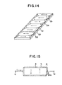
- this layer has a magnetic domain structure as shown in Fig. 14 so as to maintain a state where the sum of magnetic anisotropy energy, magnetostatic energy resulting from shape anisotropy and so forth is minimized with respect to the entire layer.
- the single magnetic layer is a rectangular thin-film magnetic layer 51 having magnetic anisotropy in its short-side or transverse direction
- magnetic domains 52 alternately reverse relative to the direction of transverse magnetization are produced in the film plane, and sequentially reverse magnetic domains 53 are produced between the ends of the adjacent magnetic domains 52 in the long-side or longitudinal direction of the magnetic layer in such a manner that a closed loop is formed with regard to the adjacent magnetic domains 52. Therefore, if an external magnetic field is applied to such magnetic layer, domain walls 54 and 55 are displaced to consequently generate Barkhausen noise.
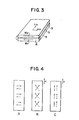
- magnetic layers 4 and 5 are superposed through a nonmagnetic intermediate layer 3 so that, when no external magnetic field is applied, the magnetic layers 4 and 5 are magnetized in mutually reverse parallel directions along the respective easy axes of magnetization as indicated by arrows Ml and M2 in Fig. 3, whereby no magnetic domain wall exists.
- the nonexistence of any domain wall has been confirmed through observation of magnetic domains by the Bitter process using a magnetic fluid.
- an external magnetic field H is gradually increased in intensity along the hard axis of magnetization of such sensing element 3, as typically shown in Fig.
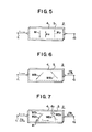
- Figs. 5 through 7 typically show merely the two magnetic layers 4 and 5 of the sensing element 2.
- the magnetic layers 4 and 5 have easy axes of magnetization in the directions indicated by e.a in Fig. 5, and a sensing current i is fed to flow in the magnetic layers 4 and 5.
- Such energization generates mutually reverse magnetic fields perpendicular to the current flow in the magnetic layers 4 and 5 opposed mutually through a nonmagnetic intermediate layer (not shown), whereby the magnetic layers 4 and 5. are magnetized as indicated by a solid-line arrow Ml and a broken-line arrow M2.
- the increases or decreases caused in the resistance variations relative to the two magnetic layers 4 and 5 by angle variations ⁇ 1 and - ⁇ 1 are coincident with each other. That is, if the resistance of one magnetic layer 4 increases, the resistance of another magnetic layer 5 also varies in the direction to increase. And a resistance variation is induced between terminals tl and t2 of the sensing element 2 due to the resistance variations in the magnetic layers 4 and 5, so that such resistance variation can be detected in the form of a voltage variation between the terminals tl and t2.
- the direction of a sensing current i to a magnetic film having a prescribed magnetic anisotropy is selectively set to coincide with the direction of applying a signal magnetic field Hs.
- the sensing element 2 comprises magnetic layers 4, 5 and a nonmagnetic intermediate layer 3 sandwiched therebetween as in the above-described invention
- the functional feature will become more obvious by comparison with an example where the direction of the sensing current i is set to be perpendicular to the direction of the signal magnetic field Hs. That is, in a state of Fig. 15 where a large current i is applied to the two magnetic layers 4 and 5 with the anisotropic magnetic field Hk thereof taken into consideration as described previously in connection with Fig.
- a magnetic field generated as a result is exerted to magnetize the magnetic layers 4 and 5 perpendicularly to the current i as indicated by a solid line and a broken line respectively.
- a signal magnetic field Hs is applied in this state perpendicularly to the current i, it coincides with the direction of magnetization caused by the current i in the magnetic layers 4 and 5, and the magnetic field Hs behaves in the same manner as in the case of application along the easy axis of magnetization. Consequently, there are generated magnetic domain walls and displacement thereof to eventually induce Barkhausen noise.
- the magnetic layer fails to be magnetized perpendicularly to the sensing current i if this current is relatively small, so that the signal magnetic field Hs comes to be applied substantially along the easy axis of magnetization as in Fig. 15, whereby an undesired result is brought with generation of Barkhausen noise.
- the magnetic layers 4 and 5 of the MR sensing element 2 are magnetostatically coupled to each other due to the presence of a nonmagnetic intermediate layer 2 sandwiched therebetween, so that exchange interaction can be neglected while a sufficiently firm magnetostatic coupling is ensured by the interaction based on the Coulomb's law, and Barkhausen noise can be eliminated with certainty as the signal magnetic field Hs and the sensing current i are directionally coincident with each other.
- the present invention is applicable to a variety of MR type magnetic heads of different structures including a nonshielded head, a shielded head, and a yoke type head where a signal magnetic flux picked up from a surface in contact with or opposed to a magnetic recording medium is introduced by means of a magnetic yoke and an MR sensing element is disposed in a cut portion formed in the magnetic yoke.
- a substrate 1 is composed of a magnetic material such as Ni-Zn ferrite, Mn-Zn ferrite or the like.
- a bias conductor 10 is formed on the layer 11 to generate a bias magnetic field when energized, and anothe insulating layer 11 is formed on the bias conductor 10 to form an MR sensing element 2.
- This element 2 extends perpendicularly to a surface 6 which is to be in contact with or opposed to a magnetic recording medium, and the bias conductor 10 is so disposed as to traverse under the MR sensing element 2.
- a front magnetic yoke 8F and a back magnetic yoke 8B are disposed anterior and posterior to the MR sensing element 2, i.e. at the two ends proximate to the surface 6 and the reverse side respectively.
- the two magnetic layers 8F and 8B are composed of a metallic material which is electrically conductive without MR effect substantially and has magnetic anisotropy perpendicular to a sensing current.
- Terminal conductive layers 9F and 9B are electrically connected to the magnetic layers 8F and 8B respectively, and terminals tl and t2 are led out therefrom.
- such layers may be superposed with a nonmagnetic intermediate layer sandwiched therebetween.
- the MR sensing element 2 can be produced in a single integrated step continuously by the technique of sputtering or vacuum evaporation. That is, the aforesaid magnetic layer 4, nonmagnetic intermediate layer 3 and magnetic layer 5 are formed in sequence by the use of a sputtering apparatus or a vacuum evaporation apparatus equipped respectively with sputter sources or evaporation sources of individual materials.
- each of the magnetic layers 4 and 5 has an easy axis of magnetization in the direction indicated by e.a and a hard axis of magnetization in the direction indicated by h.a.
- each of the magnetic layers 4 and 5 may be composed of an isotropic magnetic film having no anisotropy in its principal plane.
- the nonmagnetic intermediate layer 3 is composed of an insulating or conductive nonmagnetic material such as SiO 2 , Ti cr the like, and its thickness is selectively set to an adequate value of, e.g. 20 ⁇ so that exchange interaction is substantially not exerted between the two magnetic layers 4 and 5 and also that magnetostatic coupling is effected therebetween due to the interaction according to the Coulomb's law.
- the nonmagnetic intermediate layer 3 is so formed as to have an adequate thickness for inducing magnetostatic coupling between the two magnetic layers 4 and 5, practically the thickness required for ensuring electrical insulation is about ten times greater than the thickness selected for shutting off magnetic exchange interaction. Therefore, when reducing the thickness of the intermediate layer 3, electrical connection is substantially effected between the two magnetic layers 4 and 5. However, in case such electrical connection is not effected, it is necessary to electrically connect the terminal conductive layers 9F and 9B respectively to the magnetic layers 4 and 5. That is, in the above example, the magnetic layers 8F and 8B need to be electrically connected respectively to the magnetic layers 4 and 5 which constitute the sensing element.
- both magnetic layers are, of course, magnetostatically coupled with each other, though, the resistance change of only one magnetic layer is detected upon application of the signal magnetic layer.
- the individual layers inclusive of insulating layer 11, bias conductor 10, magnetic layers 4 and 5 of the sensing element 2, nonmagnetic intermediate layer 3, magnetic yokes 8F and 8B, terminal conductive layers 9F and 9B and so forth can be formed by sputtering or evaporation, and each can be shaped into a desired pattern by photolithography technique.
- the sensing element 2 is supplied with a dc sensing current i between its terminal conductive layers 9F and 9B, hence between the magnetic layers 8F and 8B, and a prescribed current is flowing in the bias conductor 10 so as to apply a required bias magnetic field.
- a magnetic recording medium 7 is transported perpendicularly to the drawing paper face of Fig. 1 while being kept in contact with or opposite to the surface 6, whereby a signal magnetic flux corresponding to the recorded magnetization on the medium 7 is picked up from the magnetic gap g and then is fed to the closed magnetic path formed by way of the aforesaid magnetic layer 8F - MR sensing element 2 - magnetic layer 8B - substrate 1.
- both magnetic layers 4 and 5 of the MR sensing element are formed of MR layers
- non-MR magnetic layer a magnetic layer having almost no MR effect
- the thickness and other conditions are so selected that the flux quantities of the two magnetic layers 4 and 5 become equal to each other as mentioned previously.
- the position and pattern of the bias conductor 10 may be modified in various manners, and it may be formed into a multilayer or spiral structure.
- the magnetic field to be applied is not limited to the one induced electrically, and a permanent-magnet thin film is usable as well.
- Fig. 18 graphically shows the MR characteristic of the MR sensing element according to the present invention.
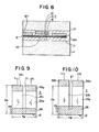
- Fig. 8 shows an example of applying the present invention to a shielded MR type magnetic head, in which a sensing element 2 is spaced apart by a predetermined distance as an insulating layer 11 is interposed between two magnetic substrates 1 and 12.
- the substrate 12 may be composed of a thin film as well.
- designated by 9F and 9B are terminal conductive layers which are electrically connected to two magnetic layers 4 and 5 superposed through a nonmagnetic intermediate layer 3.
- the discontinuous portion between the conductive layers 9F and 9B functions as the sensing element 2, and a sensing current i is fed to flow therein as shown.
- the terminal conductive layer 9F may also serve as a path for introducing a magnetic flux to the sensing element 2, and it may be composed of a conductive magnetic material having a thickness of 2000A or so.
- a type having none of such magnetic substrates 1 and 12 is termed a nonshielded MR head.
- a sensing current is fed to flow in its MR sensing element 2 perpendicularly to the track width W T as shown in Fig. 1, and the leakage magnetic field Hs from the magnetic recording medium 7 is obtained by detecting the resistance variation between the fore end and the hind end of the sensing element 2, whereby the recorded signal is reproduced.
- the track width W T corresponding to the width of the MR sensing element 2 is large, there arises a problem with respect to the signal-to-noise ratio. That is, the signal magnetic field Hs from the recording medium 7 suddenly attenuates with increase of the distance from the medium 7. such attenuation changes depending on the wavelength and tends to be greater as the wavelength becomes shorter.
- the MR sensing element 2 be disposed within the effective reach of the magnetic field from the recording medium 7. If disposed outside of such reach, the sensing element 2 fails to function properly and brings about reduction of the signal-to-noise ratio.
- the depth D E equivalent to the reach of the magnetic field from the recording medium is smaller than the track width W T and, as shown in Fig. 16, the length in the direction of the sensing current flow through substantial current-conducting terminals 19F and 19B at the two ends of the sensing element 2 is set to be equal to the depth D E . Then, there arises a disadvantage that the resistance value to be detected as a resistance variation in the MR sensing element 2 fails to be sufficiently large for easy signal processing.
- the ineffective portion is rendered large to eventually bring about reduction of the signal-to-noise ratio.
- the problem of the resistance value and that of the signal-to-noise ratio are incompatible with each other.
- the Barkhausen noise suppression effect becomes higher as the current density increases. It is therefore desired that the direction of the sensing current flow be coincident with the longitudinal direction of the MR sensing element.
- the MR sensing element 2 is divided into a plurality of regions at least on its rear side with respect to the direction of the track width and at least in the inner portion thereof within the depth D E of reach of the magnetic field from the recording medium. For example, as shown in Fig.
- the whole MR sensing element 2 is so shaped as to have a predetermined track width T W , and a slit 21 is formed at its center perpendicularly to the surface 6 which is to be in contact with or opposed to the magnetic recording medium, in such a manner as to extend over the entire area from the hind end to the fore end, or the fore end is partially left unsplit as shown in Fig. 10, whereby the MR sensing element 2 is divided into at least two MR sensing regions 2Al and 2A2.
- a coupling layer 29 being at least conductive and having a high permeability and soft magnetic property without MR effect is deposited to extend over the fore ends of such two sensing regions, and terminals tl and t2 are led out respectively from terminal conductive layers 9Bl and 9B2 which are deposited at the hind ends of such MR sensing regions 2Al and 2A2.
- the entire width of the MR sensing element 2 is sufficiently great for forming the required track width T W in the above structure, the path of a sensing current i fed between the terminals tl and t2 can be defined in the longitudinal direction of the narrowed regions 2Al and 2A2 along a signal magnetic field Hs from the magnetic recording medium.
- the coupling layer 29 may be composed of a nonmagnetic conductive material as mentioned previously, a conductive high-permeability magnetic material is usable as well. If the coupling layer is composed of a conductive high-permeability magnetic material, it becomes possible to eliminate any portion that is not sensitive to the magnetic flux between the two MR sensing regions 2Al and 2A2, thereby preventing reduction of the signal magnetic flux flowing into the MR sensing regions.
- the coupling layer 29 is formed by the use of a conductive high-permeability magnetic material, it may be shaped into a multilayer structure with a nonmagnetic intermediate layer so as to avert generation of Barkhausen noise.
- the MR sensing element 2 is shaped into a structure divided with respect to the direction of the track width, the actual path of the sensing current i can be narrowed if the track width W T is great, thereby ensuring advantages that a sufficiently large resistance value can be obtained and the current density is increasable even when the depth of the MR sensing element 2 is decreased in accordance with the depth D E of reach of the signal magnetic field.
- the MR sensing element 2 is not limited to the above examples of Figs. 9 and 10 divided into two sensing regions 2A1 and 2A2 with respect to the common track width W T . And it may be modified to a structure of Fig..11 where three or more MR sensing regions 2Al, 2A2, 2A3 .... 2An are formed for one track, and the respective fore ends and hind ends of the adjacent regions 2Al -2A2, 2A2 - 2A3 and so forth are coupled alternately to each other by means of coupling layers 29 to form a zigzag-pattern path of a sensing current i.
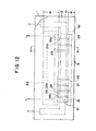
- Fig. 12 is a plan view of an exemplary yoke type head
- Fig. 13 is its sectional view taken along the line A-A.
- component members corresponding to those employed in Figs. 1, 2 and 11 are denoted by the same reference numerals, and a repeated explanation is omitted here.
- a front magnetic layer 8F and a back magnetic layer 8B extend across fore ends and hind ends of MR sensing regions 2Al, 2A2 .... 2An respectively.
- the MR sensing element 2 (2Al, 2A2 .... 2An) comprises magnetic layers 4 and 5 of NiFe alloy each having a thickness of 300 ⁇ and a nonmagnetic intermediate layer 3 of Si0 2 having a thickness of 50 ⁇ .
- the front magnetic layer 8F has a thickness of 2000A and a width (depth) W F of 3 ⁇ m while the back magnetic layer 8B also has a thickness of 2000 ⁇ and a width (depth) W B of 12 ⁇ m, and such two magnetic layers 8F and 8B are spaced spart from each other by a distance of 8 ⁇ m.
- a protective plate 12 is disposed opposite to the substrate 1. It is a matter of course that the protective plate 12 may be composed of a thin film.
- Coupling layers 29 are electrically isolated from the front magnetic layer 8F and the back magnetic layer 8B respectively through an insulating layer 11.
- the MR sensing element 2 is divided into a plurality of regions as mentioned above and the fore ends thereof are mutually separated to have a discontinuous portion within the common track width W T , it is rendered possible to achieve the same effect as in the preceding example of a single continuous track by setting the fore-end width of the slit 21 at a small valaue.
- various modifications may be contrived such as a multitrack or multichannel magnetic head structure where a plurality of MR sensing elements 2 are arrayed on a common substrate 1 with a plurality of tracks confronting the surface 6 which is to be in contact with or opposed to a common magnetic recording medium.
- the magnetic head of the present invention where its MR sensing element 2 comprises two magnetic layers 4 and 5 superposed through a nonmagnetic intermediate layer 3, application of a signal magnetic field Hs to the MR sensing element 2 is executed in the same direction as a sensing current i fed to flow therein, the magnetic layers 4 and 5 are so formed as to have anisotropy in a specific direction or to be isotropic, thereby effectively eliminating generation of Barkhausen noise to realize an improved reproducing magnetic head of a high signal-to-noise ratio. And due to the thin-film magnetic head structure, a high efficiency is achievable in mass production and multitrack MR type magnetic heads can be manufactured with facility.
Abstract
Description
- The present invention relates to a magnetoresistance effect type magnetic transducer head (hereinafter referred to as MR magnetic head).
- In the conventional MR magnetic head known heretofore, generally its sensing element comprises a single MR magnetic layer, and a sensing current is fed to flow in the plane direction of the MR magnetic layer and also in the track transverse direction of its surface to be in contact with or opposed to a magnetic recording medium so that a resistance variation, which is derived from a signal magnetic field applied to the MR magnetic layer, is detected in the form of, for example, a voltage variation. In other words, the sensing current flows in the MR magnetic layer perpendicular to the signal magnetic field applied from the magnetic recording medium. In case of using a single MR magnetic layer, the magnetic thin film has a domain structure so as to maintain a state where the sum of magnetic anisotropy energy, magnetostatic energy resulting from shape anisotropy and so forth is minimized for the entire magnetic layer. The magnetic energy is stable when the magnetic film is devided into a plurality of magnetic domain, as explained hereinafter in the present specification. When the external magnetic field is applied to the magnetic film, magnetization of the magnetic film was used by the domain wall displacement. The domain wall displacement causes the Barkhausen noise which is not desirable for reproducing operation of the magnetoresistance effect type magnetic transducer head.
- Accordingly, it is an object of the present invention to provide an improved magnetic transducer head utilizing magnetoresistance effect.
- It is another object of the present invention to provide a magnetic transducer head utilizing magnetoresistance effect which effectively avoid the generation of Barkhausen noise.
- It is further object of the present invention to provide a magnetic transducer head utilizing magnetoresistance effect having an improved signal to noise ratio.
- According to one aspect of the present invention there is provided a magnetic transducer head utilizing magnetoresistance effect which comprises a sensing element composed of first and second soft magnetic layers superposed having a non magnetic layer between the first and second soft magnetic layers, at least one of the soft magnetic layers having magnetoresistance effect and the first and second soft magnetic layers being magnetostatically coupled through the non magnetic layer,
- a pair of electrodes being connected to said sensing element at first and second end portions of the sensing element to flow a sense current through the sensing element along one direction between the first and second end portions,
- the sensing element recieving signal magnetic field parallel to said one direction, and
- the soft magnetic layers having an easy axis of magnetization substantially perpendicular to said one direction or having an isotropic magnetic characteristic in a major surface of the soft magnetic layer.
-
- Fig. 1 is a schematic enlarged plan view of an exemplary MR type magnetic head according to the present invention,
- Fig. 2 is a cross-sectional view taken along the A - A line in Fig. 1,
- Fig. 3 shows the magnetization state of a sensing element employed in the present invention,
- Figs. 4A through 4C show the magnetization state of the sensing element upon application of external magnetic field thereto,
- Figs. 5 through 7 show the operation of the magnetic transducer head according to the present invention,
- Fig. 8 is a sectional view of another magnetic transducer head according to the present invention,
- Figs. 9 through 11 show plan views of another embodiments of the sensing elements according to the present invention,
- Fig. 12 is an enlarged plan view of further embodiment of the magnetic transducer head according to the present invention,
- Fig. 13 is a sectional view taken along A - A line in Fig. 12,
- Fig. 14 is a schematic illustration of the magnetic domain structure formed in a prior art single layer MR magnetic thin film,
- Fig. 15 shows magnetization state of the sensing element for comparison MR head,
- Figs. 16 and 17 shown plan views of the sensing element used for explaining the present invention, and
- Fig. 18 is a graph showing the MR characteristics curve to explain the present invention.
- As shown in a plan view of Fig. 1 and a sectional view of Fig. 1, an MR magnetic head of the present invention is equipped, on a
substrate 1, with a thin-film sensing element 2 having magnetoresistance effect. - Denoted by a
reference numeral 6 is a surface to be in contact with or opposed to a magnetic recording medium 7, which is transported in a direction perpendicular to the drawing paper face in Fig. 1. - In the present invention, the
sensing element 2 is of a laminated structure wheremagnetic layers magnetic layers magnetic layers magnetic layers - In case the two
magnetic layers sensing element 2 are both formed of the material having magnetoresistance effect, it is desired that the twolayers - In the present invention, a signal magnetic field Hs applied from a magnetic recording medium to the
sensing element 2 and a sensing current i fed to flow in thesensing element 2 are so arranged as to act in the same direction, and each of the magnetic layers constituting thesensing element 2 is so formed as to have an easy axis of magnetization perpendicular to the signal magnetic field or to be isotropic without having anisotropy in the principal plane of the magnetic layer. - In a state where no signal magnetic field is applied to the
sensing element 2, a required bias magnetic field is applied thereto from an external source in such a manner that magnetization is effected at a predetermined angle of, e.g. 45°, to the direction of the sensing current i. - According to the above-mentioned structure of the present invention, Barkhausen noise can be effectively eliminated as will be described below.
- Referring first to the cause for generation of Barkhausen noise, in the conventional MR magnetic head where its sensing element comprises a single MR magnetic layer, this layer has a magnetic domain structure as shown in Fig. 14 so as to maintain a state where the sum of magnetic anisotropy energy, magnetostatic energy resulting from shape anisotropy and so forth is minimized with respect to the entire layer. In case the single magnetic layer is a rectangular thin-film
magnetic layer 51 having magnetic anisotropy in its short-side or transverse direction,magnetic domains 52 alternately reverse relative to the direction of transverse magnetization are produced in the film plane, and sequentially reversemagnetic domains 53 are produced between the ends of the adjacentmagnetic domains 52 in the long-side or longitudinal direction of the magnetic layer in such a manner that a closed loop is formed with regard to the adjacentmagnetic domains 52. Therefore, if an external magnetic field is applied to such magnetic layer,domain walls - In the construction of the present invention, differing from the above,
magnetic layers magnetic layers magnetic layer 5 and broken-line arrows represent that of themagnetic layer 4, the magnetization is rotated by the external magnetic field H from the mutually reverse parallel state of Fig. 4 A described in connection with Fig. 3 to the state of Fig. 4 B. And when a higher-intensity external magnetic field is applied, themagnetic layers magnetic layers magnetic layers - Now the operation of the magnetic head according to the present invention will be described below with reference to Figs. 5 through 7, which typically show merely the two
magnetic layers sensing element 2. In the initial state, themagnetic layers magnetic layers magnetic layers magnetic layers sensing element 2 along the direction of the current i, then the directions of magnetization of themagnetic layers magnetic layers layers magnetic layers magnetic layer 4 increases, the resistance of anothermagnetic layer 5 also varies in the direction to increase. And a resistance variation is induced between terminals tl and t2 of thesensing element 2 due to the resistance variations in themagnetic layers - Thus, in the present invention, the direction of a sensing current i to a magnetic film having a prescribed magnetic anisotropy is selectively set to coincide with the direction of applying a signal magnetic field Hs. With regard to such construction where the
sensing element 2 comprisesmagnetic layers magnetic layers magnetic layers magnetic layers - In the constitution of the present invention, as described above, the
magnetic layers MR sensing element 2 are magnetostatically coupled to each other due to the presence of a nonmagneticintermediate layer 2 sandwiched therebetween, so that exchange interaction can be neglected while a sufficiently firm magnetostatic coupling is ensured by the interaction based on the Coulomb's law, and Barkhausen noise can be eliminated with certainty as the signal magnetic field Hs and the sensing current i are directionally coincident with each other. - The present invention is applicable to a variety of MR type magnetic heads of different structures including a nonshielded head, a shielded head, and a yoke type head where a signal magnetic flux picked up from a surface in contact with or opposed to a magnetic recording medium is introduced by means of a magnetic yoke and an MR sensing element is disposed in a cut portion formed in the magnetic yoke.
- Hereinafter a preferred embodiment of the present invention will be described in detail with reference to Figs. 1 and 2. This embodiment represents an exemplary constitution of a yoke type MR head.
- In this example, a
substrate 1 is composed of a magnetic material such as Ni-Zn ferrite, Mn-Zn ferrite or the like. In case thesubstrate 1 is conductive, first an insulating layer 11 of Si02 or the like is formed thereon, subsequently abias conductor 10 is formed on the layer 11 to generate a bias magnetic field when energized, and anothe insulating layer 11 is formed on thebias conductor 10 to form anMR sensing element 2. Thiselement 2 extends perpendicularly to asurface 6 which is to be in contact with or opposed to a magnetic recording medium, and thebias conductor 10 is so disposed as to traverse under theMR sensing element 2. - A front
magnetic yoke 8F and a backmagnetic yoke 8B are disposed anterior and posterior to theMR sensing element 2, i.e. at the two ends proximate to thesurface 6 and the reverse side respectively. The twomagnetic layers conductive layers magnetic layers magnetic layers magnetic layer 8B is magnetically connected to themagnetic substrate 1 through a window lla bored in a nonmagnetic layer 11, so that a closed magnetic path is formed by.way of substrate 1 - frontmagnetic layer 8F - MR sensing element 2 - backmagnetic layer 8B -substrate 1. And between the fore end of the frontmagnetic layer 8F and thesubstrate 1, there is formed a magnetic gap g confronting thesurface 6 which is to be in contact with or opposed to the magnetic recording medium, and the length of such gap g is prescribed by the thickness of a nonmagnetic layer such as the insulating layer 11. - The
MR sensing element 2 can be produced in a single integrated step continuously by the technique of sputtering or vacuum evaporation. That is, the aforesaidmagnetic layer 4, nonmagnetic intermediate layer 3 andmagnetic layer 5 are formed in sequence by the use of a sputtering apparatus or a vacuum evaporation apparatus equipped respectively with sputter sources or evaporation sources of individual materials. In the example illustrated, each of themagnetic layers magnetic layers - The nonmagnetic intermediate layer 3 is composed of an insulating or conductive nonmagnetic material such as SiO2, Ti cr the like, and its thickness is selectively set to an adequate value of, e.g. 20Å so that exchange interaction is substantially not exerted between the two
magnetic layers - Although the nonmagnetic intermediate layer 3 is so formed as to have an adequate thickness for inducing magnetostatic coupling between the two
magnetic layers magnetic layers conductive layers magnetic layers magnetic layers magnetic layers - It is possible to electrically insulate the
magnetic layers - The
layers MR sensing element 2 may be formed of MR magnetic layers of the same composition and the same size and shape with uniaxial anisotropy or without anisotropy in the principal planes thereof. Such MR magnetic layers may be composed of a single metal such as Fe, Ni or Co, or an alloy of two or more thereof. - In the costitution mentioned above, the individual layers inclusive of insulating layer 11,
bias conductor 10,magnetic layers sensing element 2, nonmagnetic intermediate layer 3,magnetic yokes conductive layers - In this constitution, the
sensing element 2 is supplied with a dc sensing current i between its terminalconductive layers magnetic layers bias conductor 10 so as to apply a required bias magnetic field. In such a state, a magnetic recording medium 7 is transported perpendicularly to the drawing paper face of Fig. 1 while being kept in contact with or opposite to thesurface 6, whereby a signal magnetic flux corresponding to the recorded magnetization on the medium 7 is picked up from the magnetic gap g and then is fed to the closed magnetic path formed by way of the aforesaidmagnetic layer 8F - MR sensing element 2 -magnetic layer 8B -substrate 1. Accordingly a signal magnetic field Hs derived from the magnetic recording medium 7 is applied to theMR sensing element 2 in the same direction as the sensing current i. It follows, therefore, that the recorded signal is read out from the magnetic recording medium 7 while generation of Barkhausen noise is avoided as described above. - In addition to the foregoing example where both
magnetic layers layers magnetic layers magnetic layers magnetic layers - In addition to the above example where the
bias conductor 10 is disposed under thesensing element 2 and an external magnetic field HB is applied to thesensing element 2, the position and pattern of thebias conductor 10 may be modified in various manners, and it may be formed into a multilayer or spiral structure. Furthermore, the magnetic field to be applied is not limited to the one induced electrically, and a permanent-magnet thin film is usable as well. Fig. 18 graphically shows the MR characteristic of the MR sensing element according to the present invention. The curve represents the characteristic obtained when a sensing current of 10 mA is fed to flow in the sensing element of 4 µm x 4 µm where magnetic layers of Ni-Fe alloy having a thickness of 300A are superposed through an intermediate layer of Si02 having a thickness of 40h, and a magnetic field is applied in the same direction as the sensing current. In this case, each of the magnetic layers is composed of an isotropic film having no magnetic anisotropy in its plane. AS is apparent from the graph, there is no generation of Barkhausen noise. - Besides the above example of a yoke type structure where a closed magnetic path including the
sensing element 2 is forced by themagnetic substrate 1 and themagnetic layers sensing element 2 substantially confronts the magnetic recording medium, or to a single pole structure where a closed magnetic path is not formed by the magnetic head itself. - Fig. 8 shows an example of applying the present invention to a shielded MR type magnetic head, in which a
sensing element 2 is spaced apart by a predetermined distance as an insulating layer 11 is interposed between twomagnetic substrates substrate 12 may be composed of a thin film as well. In the figure, designated by 9F and 9B are terminal conductive layers which are electrically connected to twomagnetic layers conductive layers sensing element 2, and a sensing current i is fed to flow therein as shown. The terminalconductive layer 9F may also serve as a path for introducing a magnetic flux to thesensing element 2, and it may be composed of a conductive magnetic material having a thickness of 2000A or so. - Relative to this example, a type having none of such
magnetic substrates - In the magnetic head of the present invention, a sensing current is fed to flow in its
MR sensing element 2 perpendicularly to the track width WT as shown in Fig. 1, and the leakage magnetic field Hs from the magnetic recording medium 7 is obtained by detecting the resistance variation between the fore end and the hind end of thesensing element 2, whereby the recorded signal is reproduced. In this stage, if the track width WT corresponding to the width of theMR sensing element 2 is large, there arises a problem with respect to the signal-to-noise ratio. That is, the signal magnetic field Hs from the recording medium 7 suddenly attenuates with increase of the distance from the medium 7. such attenuation changes depending on the wavelength and tends to be greater as the wavelength becomes shorter. It is desired that theMR sensing element 2 be disposed within the effective reach of the magnetic field from the recording medium 7. If disposed outside of such reach, thesensing element 2 fails to function properly and brings about reduction of the signal-to-noise ratio. Suppose now that the depth DE equivalent to the reach of the magnetic field from the recording medium is smaller than the track width WT and, as shown in Fig. 16, the length in the direction of the sensing current flow through substantial current-conductingterminals sensing element 2 is set to be equal to the depth DE. Then, there arises a disadvantage that the resistance value to be detected as a resistance variation in theMR sensing element 2 fails to be sufficiently large for easy signal processing. To the contrary, if the above length of theMR sensing element 2 is set to be greater than the reach of the magnetic field from the recording medium as shown in Fig. 17, the ineffective portion is rendered large to eventually bring about reduction of the signal-to-noise ratio. Thus, the problem of the resistance value and that of the signal-to-noise ratio are incompatible with each other. Meanwhile, the Barkhausen noise suppression effect becomes higher as the current density increases. It is therefore desired that the direction of the sensing current flow be coincident with the longitudinal direction of the MR sensing element. - For solving the problems of the aforesaid resistance vlaue, signal-to-noise ratio and current density in such a case where the track width WT is greater than the depth DE of reach of the magnetic field from the recording medium, the
MR sensing element 2 is divided into a plurality of regions at least on its rear side with respect to the direction of the track width and at least in the inner portion thereof within the depth DE of reach of the magnetic field from the recording medium. For example, as shown in Fig. 9, the wholeMR sensing element 2 is so shaped as to have a predetermined track width TW, and aslit 21 is formed at its center perpendicularly to thesurface 6 which is to be in contact with or opposed to the magnetic recording medium, in such a manner as to extend over the entire area from the hind end to the fore end, or the fore end is partially left unsplit as shown in Fig. 10, whereby theMR sensing element 2 is divided into at least two MR sensing regions 2Al and 2A2. Acoupling layer 29 being at least conductive and having a high permeability and soft magnetic property without MR effect is deposited to extend over the fore ends of such two sensing regions, and terminals tl and t2 are led out respectively from terminal conductive layers 9Bl and 9B2 which are deposited at the hind ends of such MR sensing regions 2Al and 2A2. Although the entire width of theMR sensing element 2 is sufficiently great for forming the required track width TW in the above structure, the path of a sensing current i fed between the terminals tl and t2 can be defined in the longitudinal direction of the narrowed regions 2Al and 2A2 along a signal magnetic field Hs from the magnetic recording medium. Although thecoupling layer 29 may be composed of a nonmagnetic conductive material as mentioned previously, a conductive high-permeability magnetic material is usable as well. If the coupling layer is composed of a conductive high-permeability magnetic material, it becomes possible to eliminate any portion that is not sensitive to the magnetic flux between the two MR sensing regions 2Al and 2A2, thereby preventing reduction of the signal magnetic flux flowing into the MR sensing regions. When thecoupling layer 29 is formed by the use of a conductive high-permeability magnetic material, it may be shaped into a multilayer structure with a nonmagnetic intermediate layer so as to avert generation of Barkhausen noise. - In case the
MR sensing element 2 is shaped into a structure divided with respect to the direction of the track width, the actual path of the sensing current i can be narrowed if the track width WT is great, thereby ensuring advantages that a sufficiently large resistance value can be obtained and the current density is increasable even when the depth of theMR sensing element 2 is decreased in accordance with the depth DE of reach of the signal magnetic field. - The
MR sensing element 2 is not limited to the above examples of Figs. 9 and 10 divided into two sensing regions 2A1 and 2A2 with respect to the common track width WT. And it may be modified to a structure of Fig..11 where three or more MR sensing regions 2Al, 2A2, 2A3 .... 2An are formed for one track, and the respective fore ends and hind ends of the adjacent regions 2Al -2A2, 2A2 - 2A3 and so forth are coupled alternately to each other by means of coupling layers 29 to form a zigzag-pattern path of a sensing current i. - Thus, even with a modified magnetic head structure where a common track is shaped by two or more MR sensing regions 2Al, 2A2 and so forth, it is also possible to constitute a shielded, nonshielded or yoke type head as in the foregoing embodiment having a
single sensing element 2. Fig. 12 is a plan view of an exemplary yoke type head, and Fig. 13 is its sectional view taken along the line A-A. In Figs. 12 and 13, component members corresponding to those employed in Figs. 1, 2 and 11 are denoted by the same reference numerals, and a repeated explanation is omitted here. In this embodiment, a frontmagnetic layer 8F and a backmagnetic layer 8B extend across fore ends and hind ends of MR sensing regions 2Al, 2A2 .... 2An respectively. In such constitution, the MR sensing element 2 (2Al, 2A2 .... 2An) comprisesmagnetic layers magnetic layer 8F has a thickness of 2000A and a width (depth) WF of 3 µm while the backmagnetic layer 8B also has a thickness of 2000Å and a width (depth) WB of 12 µm, and such twomagnetic layers protective plate 12 is disposed opposite to thesubstrate 1. It is a matter of course that theprotective plate 12 may be composed of a thin film. Coupling layers 29 are electrically isolated from the frontmagnetic layer 8F and the backmagnetic layer 8B respectively through an insulating layer 11. In case theMR sensing element 2 is divided into a plurality of regions as mentioned above and the fore ends thereof are mutually separated to have a discontinuous portion within the common track width WT, it is rendered possible to achieve the same effect as in the preceding example of a single continuous track by setting the fore-end width of theslit 21 at a small valaue. - In addition to the illustrated embodiments where the magnetic head has a single track, various modifications may be contrived such as a multitrack or multichannel magnetic head structure where a plurality of
MR sensing elements 2 are arrayed on acommon substrate 1 with a plurality of tracks confronting thesurface 6 which is to be in contact with or opposed to a common magnetic recording medium. - In the magnetic head of the present invention where its
MR sensing element 2 comprises twomagnetic layers MR sensing element 2 is executed in the same direction as a sensing current i fed to flow therein, themagnetic layers
Claims (14)
Applications Claiming Priority (2)
| Application Number | Priority Date | Filing Date | Title |
|---|---|---|---|
| JP60247752A JPH07105006B2 (en) | 1985-11-05 | 1985-11-05 | Magnetoresistive magnetic head |
| JP247752/85 | 1985-11-05 |
Publications (3)
| Publication Number | Publication Date |
|---|---|
| EP0221540A2 true EP0221540A2 (en) | 1987-05-13 |
| EP0221540A3 EP0221540A3 (en) | 1991-03-27 |
| EP0221540B1 EP0221540B1 (en) | 1994-08-24 |
Family
ID=17168137
Family Applications (1)
| Application Number | Title | Priority Date | Filing Date |
|---|---|---|---|
| EP86115284A Expired - Lifetime EP0221540B1 (en) | 1985-11-05 | 1986-11-04 | Magnetic transducer head utilizing magnetoresistance effect |
Country Status (5)
| Country | Link |
|---|---|
| US (1) | US4896235A (en) |
| EP (1) | EP0221540B1 (en) |
| JP (1) | JPH07105006B2 (en) |
| CA (1) | CA1281132C (en) |
| DE (1) | DE3650040T2 (en) |
Cited By (15)
| Publication number | Priority date | Publication date | Assignee | Title |
|---|---|---|---|---|
| EP0298417A1 (en) * | 1987-07-09 | 1989-01-11 | International Business Machines Corporation | A magnetoresistive read transducer |
| DE3820475C1 (en) * | 1988-06-16 | 1989-12-21 | Kernforschungsanlage Juelich Gmbh, 5170 Juelich, De | |
| EP0430672A2 (en) * | 1989-11-29 | 1991-06-05 | International Business Machines Corporation | Magnetoresistive transducer |
| EP0457278A2 (en) * | 1990-05-16 | 1991-11-21 | Sony Corporation | Magnetoresistance effect type thin film magnetic head |
| EP0477941A1 (en) * | 1990-09-28 | 1992-04-01 | Sony Corporation | Magneto-resistance effect type magnetic head |
| EP0498668A2 (en) * | 1991-02-08 | 1992-08-12 | International Business Machines Corporation | Magnetoresistive sensor |
| US5155644A (en) * | 1985-12-27 | 1992-10-13 | Sharp Kabushiki Kaisha | Yoke thin film magnetic head constructed to avoid Barkhausen noises |
| US5247413A (en) * | 1990-05-16 | 1993-09-21 | Sony Corporation | Magnetoresistance effect type thin film magnetic head with noise reducing electrode |
| EP0613120A2 (en) * | 1993-02-26 | 1994-08-31 | Sony Corporation | Magnetoresistance thin film magnetic head and bias characteristics measuring method |
| EP0616484A1 (en) * | 1993-03-19 | 1994-09-21 | Thomson-Csf | Magnetoresistive transducer und manufacturing method |
| EP0651374A2 (en) * | 1993-11-01 | 1995-05-03 | Hewlett-Packard Company | A planar magnetoresistive head |
| EP0652550A1 (en) * | 1993-11-08 | 1995-05-10 | Commissariat A L'energie Atomique | Read-out magnetic head with multilayer magnetoresistant element and concentrator and manufacturing method |
| EP0654782A2 (en) * | 1993-11-22 | 1995-05-24 | Koninklijke Philips Electronics N.V. | Magnetic head having a head face and a thin-film structure, and method of manufacturing the magnetic head |
| EP0751498A2 (en) * | 1995-06-29 | 1997-01-02 | Sony Corporation | Thin-film magnetic head and method for producing same |
| US5822159A (en) * | 1993-07-14 | 1998-10-13 | Sony Corporation | Thin-film magnetic head, magnetoresistance effect magnetic head and composite magnetic head |
Families Citing this family (31)
| Publication number | Priority date | Publication date | Assignee | Title |
|---|---|---|---|---|
| US5218497A (en) * | 1988-12-02 | 1993-06-08 | Hitachi, Ltd. | Magnetic recording-reproducing apparatus and magnetoresistive head having two or more magnetoresistive films for use therewith |
| JPH02124575U (en) * | 1989-03-24 | 1990-10-15 | ||
| FR2648942B1 (en) * | 1989-06-27 | 1995-08-11 | Thomson Csf | SENSOR WITH MAGNETORESISTIVE EFFECT |
| US5027243A (en) * | 1989-11-27 | 1991-06-25 | Hewlett-Packard Company | Self-initialization of short magnetoresistive sensors into a single domain state |
| US5155642A (en) * | 1989-11-29 | 1992-10-13 | International Business Machines Corporation | Anisotropy configuration for longitudinally constrained magnetoresistive transducers |
| NL9000546A (en) * | 1990-03-09 | 1991-10-01 | Philips Nv | METHOD FOR MANUFACTURING A THIN-FILM MAGNETIC HEAD AND A THIN-FILM MAGNETIC HEAD MANUFACTURABLE ACCORDING TO THE METHOD |
| US5084794A (en) * | 1990-03-29 | 1992-01-28 | Eastman Kodak Company | Shorted dual element magnetoresistive reproduce head exhibiting high density signal amplification |
| US5390061A (en) | 1990-06-08 | 1995-02-14 | Hitachi, Ltd. | Multilayer magnetoresistance effect-type magnetic head |
| JPH0512628A (en) * | 1991-07-02 | 1993-01-22 | Sony Corp | Composite thin film head |
| US5341261A (en) * | 1991-08-26 | 1994-08-23 | International Business Machines Corporation | Magnetoresistive sensor having multilayer thin film structure |
| US5301079A (en) * | 1992-11-17 | 1994-04-05 | International Business Machines Corporation | Current biased magnetoresistive spin valve sensor |
| US5485333A (en) * | 1993-04-23 | 1996-01-16 | Eastman Kodak Company | Shorted DMR reproduce head |
| TW265440B (en) * | 1993-04-30 | 1995-12-11 | Ibm | |
| DE4319146C2 (en) * | 1993-06-09 | 1999-02-04 | Inst Mikrostrukturtechnologie | Magnetic field sensor, made up of a magnetic reversal line and one or more magnetoresistive resistors |
| SG49605A1 (en) * | 1993-06-18 | 1998-06-15 | Ibm | Magnetoresistive film method of its fabrication and magnetoresistive sensor |
| FR2709600B1 (en) * | 1993-09-02 | 1995-09-29 | Commissariat Energie Atomique | Magnetoresistive component and sensor with repeated geometric pattern. |
| US5452163A (en) * | 1993-12-23 | 1995-09-19 | International Business Machines Corporation | Multilayer magnetoresistive sensor |
| DE69510382T2 (en) * | 1994-01-12 | 2000-01-13 | Eastman Kodak Co | Dual magnetoresistive playback head with magnetic shielding and method for its production |
| DE69511145T2 (en) * | 1994-03-09 | 2000-02-03 | Eastman Kodak Co | Magnetoresistive playback head with double spin valve element |
| US5500590A (en) * | 1994-07-20 | 1996-03-19 | Honeywell Inc. | Apparatus for sensing magnetic fields using a coupled film magnetoresistive transducer |
| US5557491A (en) * | 1994-08-18 | 1996-09-17 | International Business Machines Corporation | Two terminal single stripe orthogonal MR head having biasing conductor integral with the lead layers |
| US5898546A (en) * | 1994-09-08 | 1999-04-27 | Fujitsu Limited | Magnetoresistive head and magnetic recording apparatus |
| US5493467A (en) * | 1994-12-27 | 1996-02-20 | International Business Machines Corporation | Yoke spin valve MR read head |
| US6510031B1 (en) * | 1995-03-31 | 2003-01-21 | International Business Machines Corporation | Magnetoresistive sensor with magnetostatic coupling to obtain opposite alignment of magnetic regions |
| EP0777213A1 (en) * | 1995-11-29 | 1997-06-04 | Eastman Kodak Company | Flux-guided paired magnetoresistive head |
| US6747854B1 (en) * | 1997-02-20 | 2004-06-08 | Koninklijke Philips Electronics N.V. | Multi-channel magnetic head with magnetoresistive elements |
| US6031695A (en) | 1997-09-05 | 2000-02-29 | International Business Machines Corporation | Combined read head and write head with non-magnetic electrically conductive layer on upper pole tip thereof |
| US7227726B1 (en) | 2002-11-12 | 2007-06-05 | Storage Technology Corporation | Method and system for providing a dual-stripe magnetoresistive element having periodic structure stabilization |
| EP1544578A2 (en) * | 2003-12-18 | 2005-06-22 | Hitachi, Ltd. | Rotation angle sensor |
| US7505233B2 (en) * | 2004-12-15 | 2009-03-17 | International Business Machines Corporation | Magnetic sensor |
| JP6958587B2 (en) * | 2019-03-12 | 2021-11-02 | Tdk株式会社 | Magnetic flux absorber and magnetic sensor equipped with it |
Citations (9)
| Publication number | Priority date | Publication date | Assignee | Title |
|---|---|---|---|---|
| JPS5223924A (en) * | 1975-08-19 | 1977-02-23 | Matsushita Electric Ind Co Ltd | Magnetic flux response type magnetic head |
| JPS52134420A (en) * | 1976-05-04 | 1977-11-10 | Nec Corp | Magnetic head |
| JPS5637823A (en) * | 1979-09-03 | 1981-04-11 | Mitsubishi Electric Corp | Thin-film magnetic resistance head |
| US4356523A (en) * | 1980-06-09 | 1982-10-26 | Ampex Corporation | Narrow track magnetoresistive transducer assembly |
| US4438470A (en) * | 1981-07-20 | 1984-03-20 | Canon Kabushiki Kaisha | Magnetic head of magnetic reluctance effect type and a method for making the same |
| JPS59168916A (en) * | 1983-03-17 | 1984-09-22 | Fujitsu Ltd | Magneto-resistance effect type magnetic head |
| EP0154005A2 (en) * | 1984-02-28 | 1985-09-11 | International Business Machines Corporation | Twin track vertical read-write head structure |
| JPS61182620A (en) * | 1985-02-07 | 1986-08-15 | Matsushita Electric Ind Co Ltd | Thin film magnetic head |
| EP0218814A1 (en) * | 1985-10-02 | 1987-04-22 | International Business Machines Corporation | Differential twin track vertical read/write magnetic head structure |
Family Cites Families (5)
| Publication number | Priority date | Publication date | Assignee | Title |
|---|---|---|---|---|
| US3860965A (en) * | 1973-10-04 | 1975-01-14 | Ibm | Magnetoresistive read head assembly having matched elements for common mode rejection |
| US3864751A (en) * | 1973-10-04 | 1975-02-04 | Ibm | Induced bias magnetoresistive read transducer |
| US4034414A (en) * | 1974-12-04 | 1977-07-05 | Matsushita Electric Industrial Co., Ltd. | Magnetic head |
| CA1209260A (en) * | 1982-10-29 | 1986-08-05 | Tetsuo Sekiya | Magnetic transducer head using magnetroresistance effect |
| US4668913A (en) * | 1985-03-14 | 1987-05-26 | International Business Machines Corporation | Constant flux magneto resistive magnetic reluctance sensing apparatus |
-
1985
- 1985-11-05 JP JP60247752A patent/JPH07105006B2/en not_active Expired - Fee Related
-
1986
- 1986-11-04 DE DE3650040T patent/DE3650040T2/en not_active Expired - Fee Related
- 1986-11-04 CA CA000522155A patent/CA1281132C/en not_active Expired - Lifetime
- 1986-11-04 EP EP86115284A patent/EP0221540B1/en not_active Expired - Lifetime
-
1989
- 1989-01-17 US US07/298,299 patent/US4896235A/en not_active Expired - Lifetime
Patent Citations (9)
| Publication number | Priority date | Publication date | Assignee | Title |
|---|---|---|---|---|
| JPS5223924A (en) * | 1975-08-19 | 1977-02-23 | Matsushita Electric Ind Co Ltd | Magnetic flux response type magnetic head |
| JPS52134420A (en) * | 1976-05-04 | 1977-11-10 | Nec Corp | Magnetic head |
| JPS5637823A (en) * | 1979-09-03 | 1981-04-11 | Mitsubishi Electric Corp | Thin-film magnetic resistance head |
| US4356523A (en) * | 1980-06-09 | 1982-10-26 | Ampex Corporation | Narrow track magnetoresistive transducer assembly |
| US4438470A (en) * | 1981-07-20 | 1984-03-20 | Canon Kabushiki Kaisha | Magnetic head of magnetic reluctance effect type and a method for making the same |
| JPS59168916A (en) * | 1983-03-17 | 1984-09-22 | Fujitsu Ltd | Magneto-resistance effect type magnetic head |
| EP0154005A2 (en) * | 1984-02-28 | 1985-09-11 | International Business Machines Corporation | Twin track vertical read-write head structure |
| JPS61182620A (en) * | 1985-02-07 | 1986-08-15 | Matsushita Electric Ind Co Ltd | Thin film magnetic head |
| EP0218814A1 (en) * | 1985-10-02 | 1987-04-22 | International Business Machines Corporation | Differential twin track vertical read/write magnetic head structure |
Non-Patent Citations (4)
| Title |
|---|
| PATENT ABSTRACTS OF JAPAN, vol. 1, no. 88 (E-77)[2116], 16th August 1977; & JP,A,52 023 924 (MATSUSHITA DENKI SANGYO K.K.) 23-02-1977; The whole document. * |
| PATENT ABSTRACTS OF JAPAN, vol. 2, no. 17, 6th February 1978, page 10970 E77; & JP,A,52 134 420 (NIPPON DENKI K.K.) 10-11-1977; The whole document. * |
| PATENT ABSTRACTS OF JAPAN, vol. 5, no. 92 (P-66)[764], 16th June 1981; & JP,A,56 037 823 (MITSUBISHI DENKI K.K.) 11-04-1981; The whole document. * |
| PATENT ABSTRACTS OF JAPAN, vol. 9, no. 24 (P-331)[1747], 31st January 1985; & JP,A,59 168 916 (FUJITSU K.K.) 22-09-1984; The whole document. * |
Cited By (31)
| Publication number | Priority date | Publication date | Assignee | Title |
|---|---|---|---|---|
| US5155644A (en) * | 1985-12-27 | 1992-10-13 | Sharp Kabushiki Kaisha | Yoke thin film magnetic head constructed to avoid Barkhausen noises |
| EP0298417A1 (en) * | 1987-07-09 | 1989-01-11 | International Business Machines Corporation | A magnetoresistive read transducer |
| DE3820475C1 (en) * | 1988-06-16 | 1989-12-21 | Kernforschungsanlage Juelich Gmbh, 5170 Juelich, De | |
| EP0430672A2 (en) * | 1989-11-29 | 1991-06-05 | International Business Machines Corporation | Magnetoresistive transducer |
| EP0430672A3 (en) * | 1989-11-29 | 1993-10-13 | International Business Machines Corporation | Magnetoresistive transducer |
| EP0457278A2 (en) * | 1990-05-16 | 1991-11-21 | Sony Corporation | Magnetoresistance effect type thin film magnetic head |
| EP0457278A3 (en) * | 1990-05-16 | 1992-08-05 | Sony Corporation | Magnetoresistance effect type thin film magnetic head |
| US5247413A (en) * | 1990-05-16 | 1993-09-21 | Sony Corporation | Magnetoresistance effect type thin film magnetic head with noise reducing electrode |
| EP0477941A1 (en) * | 1990-09-28 | 1992-04-01 | Sony Corporation | Magneto-resistance effect type magnetic head |
| US5272582A (en) * | 1990-09-28 | 1993-12-21 | Sony Corporation | Magneto-resistance effect magnetic head with static electricity protection |
| EP0498668A2 (en) * | 1991-02-08 | 1992-08-12 | International Business Machines Corporation | Magnetoresistive sensor |
| EP0498668A3 (en) * | 1991-02-08 | 1993-10-13 | International Business Machines Corporation | Magnetoresistive sensor |
| EP0613120A2 (en) * | 1993-02-26 | 1994-08-31 | Sony Corporation | Magnetoresistance thin film magnetic head and bias characteristics measuring method |
| US5875078A (en) * | 1993-02-26 | 1999-02-23 | Sony Corporation | Magnetoresistance thin film magnetic head having reduced terminal count; and bias characteristics measuring method |
| EP0613120A3 (en) * | 1993-02-26 | 1996-03-20 | Sony Corp | Magnetoresistance thin film magnetic head and bias characteristics measuring method. |
| FR2702919A1 (en) * | 1993-03-19 | 1994-09-23 | Thomson Csf | Magnetoresistive transducer and method of making |
| EP0616484A1 (en) * | 1993-03-19 | 1994-09-21 | Thomson-Csf | Magnetoresistive transducer und manufacturing method |
| US5474833A (en) * | 1993-03-19 | 1995-12-12 | Thomson-Csf | Magnetoresistive transducer and method of manufacture |
| US5872691A (en) * | 1993-07-14 | 1999-02-16 | Sony Corporation | Thin film magnetic head, magnetoresistance effect magnetic head and composite magnetic head |
| US5822159A (en) * | 1993-07-14 | 1998-10-13 | Sony Corporation | Thin-film magnetic head, magnetoresistance effect magnetic head and composite magnetic head |
| EP0651374A3 (en) * | 1993-11-01 | 1995-09-06 | Hewlett Packard Co | A planar magnetoresistive head. |
| US5491606A (en) * | 1993-11-01 | 1996-02-13 | Hesterman; Victor W. | Planar magnetoresistive head with an improved gap structure |
| EP0651374A2 (en) * | 1993-11-01 | 1995-05-03 | Hewlett-Packard Company | A planar magnetoresistive head |
| US5764448A (en) * | 1993-11-08 | 1998-06-09 | Commissariat A L'energie Atomique | Magnetic read head having a multilayer magnetoresistant element and a concentrator, as well as its production process |
| FR2712420A1 (en) * | 1993-11-08 | 1995-05-19 | Commissariat Energie Atomique | Multilayer magneto-resistive magnetic element readout head and concentrator and method for producing the same. |
| EP0652550A1 (en) * | 1993-11-08 | 1995-05-10 | Commissariat A L'energie Atomique | Read-out magnetic head with multilayer magnetoresistant element and concentrator and manufacturing method |
| EP0654782A3 (en) * | 1993-11-22 | 1995-06-21 | Philips Electronics Nv | Magnetic head having a head face and a thin-film structure, and method of manufacturing the magnetic head. |
| BE1007775A3 (en) * | 1993-11-22 | 1995-10-17 | Philips Electronics Nv | MAGNETIC HEAD, PROVIDED WITH A HEAD SURFACE AND A THIN FILM STRUCTURE, AND METHOD FOR MANUFACTURING THE MAGNETIC HEAD. |
| EP0654782A2 (en) * | 1993-11-22 | 1995-05-24 | Koninklijke Philips Electronics N.V. | Magnetic head having a head face and a thin-film structure, and method of manufacturing the magnetic head |
| EP0751498A3 (en) * | 1995-06-29 | 1998-05-13 | Sony Corporation | Thin-film magnetic head and method for producing same |
| EP0751498A2 (en) * | 1995-06-29 | 1997-01-02 | Sony Corporation | Thin-film magnetic head and method for producing same |
Also Published As
| Publication number | Publication date |
|---|---|
| JPS62234218A (en) | 1987-10-14 |
| DE3650040D1 (en) | 1994-09-29 |
| EP0221540A3 (en) | 1991-03-27 |
| CA1281132C (en) | 1991-03-05 |
| DE3650040T2 (en) | 1995-04-20 |
| JPH07105006B2 (en) | 1995-11-13 |
| EP0221540B1 (en) | 1994-08-24 |
| US4896235A (en) | 1990-01-23 |
Similar Documents
| Publication | Publication Date | Title |
|---|---|---|
| US4896235A (en) | Magnetic transducer head utilizing magnetoresistance effect | |
| US4816947A (en) | Single track vertical and horizontal recording read/write head design | |
| US5402292A (en) | Magnetoresistance effect type thin film magnetic head using high coercion films | |
| US6018443A (en) | Thin film magnetic head having hard films for magnetizing a shield layer in a single domain state | |
| US5436779A (en) | Integrated yoke magnetoresistive transducer with magnetic shunt | |
| US6101067A (en) | Thin film magnetic head with a particularly shaped magnetic pole piece and spaced relative to an MR element | |
| JPH1186218A (en) | Thin film magnetic head | |
| US5412524A (en) | Magneto-resistive head | |
| EP0702357B1 (en) | Magneto-resistance effect head and magnetic recording/reproducing head thereof | |
| US5808843A (en) | Magnetoresistance effect reproduction head | |
| US5581427A (en) | Peak enhanced magnetoresistive read transducer | |
| US5748413A (en) | Magnetoresistive reas transducer with exchange biasing of magnetoresistive sensor and soft adjacent layer | |
| KR100267411B1 (en) | Magnetoresistive head | |
| EP0613120B1 (en) | Magnetoresistance thin film magnetic head | |
| EP0482642B1 (en) | Composite magnetoresistive thin-film magnetic head | |
| JPH0473210B2 (en) | ||
| JP2508475B2 (en) | Magnetoresistive magnetic head | |
| JP2596010B2 (en) | Magnetoresistive magnetic head | |
| JP2642923B2 (en) | Magnetoresistive magnetic head | |
| JP3233115B2 (en) | Magnetoresistive head and method of manufacturing the same | |
| JPH09115112A (en) | Magnetoresistive element and its production and magnetic head | |
| JPH05266437A (en) | Magnetoresistance effect type head | |
| JPS63181108A (en) | Magneto-resistance effect type magnetic head | |
| JPS62159318A (en) | Magneto-resistance effect type magnetic sensor | |
| JPH0830925A (en) | Magneto-resistance effect type thin-film magnetic head |
Legal Events
| Date | Code | Title | Description |
|---|---|---|---|
| PUAI | Public reference made under article 153(3) epc to a published international application that has entered the european phase |
Free format text: ORIGINAL CODE: 0009012 |
|
| AK | Designated contracting states |
Kind code of ref document: A2 Designated state(s): DE FR GB NL |
|
| PUAL | Search report despatched |
Free format text: ORIGINAL CODE: 0009013 |
|
| 17P | Request for examination filed |
Effective date: 19901220 |
|
| AK | Designated contracting states |
Kind code of ref document: A3 Designated state(s): DE FR GB NL |
|
| 17Q | First examination report despatched |
Effective date: 19920219 |
|
| GRAA | (expected) grant |
Free format text: ORIGINAL CODE: 0009210 |
|
| AK | Designated contracting states |
Kind code of ref document: B1 Designated state(s): DE FR GB NL |
|
| REF | Corresponds to: |
Ref document number: 3650040 Country of ref document: DE Date of ref document: 19940929 |
|
| ET | Fr: translation filed | ||
| PLBE | No opposition filed within time limit |
Free format text: ORIGINAL CODE: 0009261 |
|
| STAA | Information on the status of an ep patent application or granted ep patent |
Free format text: STATUS: NO OPPOSITION FILED WITHIN TIME LIMIT |
|
| 26N | No opposition filed | ||
| PGFP | Annual fee paid to national office [announced via postgrant information from national office to epo] |
Ref country code: GB Payment date: 20011107 Year of fee payment: 16 |
|
| PGFP | Annual fee paid to national office [announced via postgrant information from national office to epo] |
Ref country code: FR Payment date: 20011113 Year of fee payment: 16 |
|
| PGFP | Annual fee paid to national office [announced via postgrant information from national office to epo] |
Ref country code: DE Payment date: 20011119 Year of fee payment: 16 |
|
| PGFP | Annual fee paid to national office [announced via postgrant information from national office to epo] |
Ref country code: NL Payment date: 20011129 Year of fee payment: 16 |
|
| REG | Reference to a national code |
Ref country code: GB Ref legal event code: IF02 |
|
| PG25 | Lapsed in a contracting state [announced via postgrant information from national office to epo] |
Ref country code: GB Free format text: LAPSE BECAUSE OF NON-PAYMENT OF DUE FEES Effective date: 20021104 |
|
| PG25 | Lapsed in a contracting state [announced via postgrant information from national office to epo] |
Ref country code: NL Free format text: LAPSE BECAUSE OF NON-PAYMENT OF DUE FEES Effective date: 20030601 |
|
| PG25 | Lapsed in a contracting state [announced via postgrant information from national office to epo] |
Ref country code: DE Free format text: LAPSE BECAUSE OF NON-PAYMENT OF DUE FEES Effective date: 20030603 |
|
| GBPC | Gb: european patent ceased through non-payment of renewal fee | ||
| PG25 | Lapsed in a contracting state [announced via postgrant information from national office to epo] |
Ref country code: FR Free format text: LAPSE BECAUSE OF NON-PAYMENT OF DUE FEES Effective date: 20030731 |
|
| NLV4 | Nl: lapsed or anulled due to non-payment of the annual fee |
Effective date: 20030601 |
|
| REG | Reference to a national code |
Ref country code: FR Ref legal event code: ST |