EP0226205A2 - Method of relocating data in and extending life of a memory system - Google Patents
Method of relocating data in and extending life of a memory system Download PDFInfo
- Publication number
- EP0226205A2 EP0226205A2 EP86117469A EP86117469A EP0226205A2 EP 0226205 A2 EP0226205 A2 EP 0226205A2 EP 86117469 A EP86117469 A EP 86117469A EP 86117469 A EP86117469 A EP 86117469A EP 0226205 A2 EP0226205 A2 EP 0226205A2
- Authority
- EP
- European Patent Office
- Prior art keywords
- data
- memory
- block
- memory block
- storing
- Prior art date
- Legal status (The legal status is an assumption and is not a legal conclusion. Google has not performed a legal analysis and makes no representation as to the accuracy of the status listed.)
- Granted
Links
Images


Classifications
-
- G—PHYSICS
- G11—INFORMATION STORAGE
- G11C—STATIC STORES
- G11C29/00—Checking stores for correct operation ; Subsequent repair; Testing stores during standby or offline operation
- G11C29/70—Masking faults in memories by using spares or by reconfiguring
- G11C29/74—Masking faults in memories by using spares or by reconfiguring using duplex memories, i.e. using dual copies
-
- G—PHYSICS
- G07—CHECKING-DEVICES
- G07B—TICKET-ISSUING APPARATUS; FARE-REGISTERING APPARATUS; FRANKING APPARATUS
- G07B17/00—Franking apparatus
- G07B17/00185—Details internally of apparatus in a franking system, e.g. franking machine at customer or apparatus at post office
- G07B17/00362—Calculation or computing within apparatus, e.g. calculation of postage value
-
- G—PHYSICS
- G06—COMPUTING; CALCULATING OR COUNTING
- G06F—ELECTRIC DIGITAL DATA PROCESSING
- G06F11/00—Error detection; Error correction; Monitoring
- G06F11/07—Responding to the occurrence of a fault, e.g. fault tolerance
- G06F11/16—Error detection or correction of the data by redundancy in hardware
- G06F11/1666—Error detection or correction of the data by redundancy in hardware where the redundant component is memory or memory area
- G06F11/167—Error detection by comparing the memory output
-
- G—PHYSICS
- G07—CHECKING-DEVICES
- G07B—TICKET-ISSUING APPARATUS; FARE-REGISTERING APPARATUS; FRANKING APPARATUS
- G07B17/00—Franking apparatus
- G07B17/00185—Details internally of apparatus in a franking system, e.g. franking machine at customer or apparatus at post office
- G07B17/00362—Calculation or computing within apparatus, e.g. calculation of postage value
- G07B2017/00395—Memory organization
- G07B2017/00411—Redundant storage, e.g. back-up of registers
Definitions
- the present invention relates to improved electronic memory systems and more particularly to an improved electronic memory system incorporated into electronic postage meters for the purpose of maintaining a running account of the functions performed by the postage meter, particularly the accumulated amount of postage dispensed by the postage meter.
- postal meters on the market today are rental devices.
- the meters are rented by the customer and usually retained and used on the premises of the customer.
- Routine servicing of the meter such as taking readings of the registers and/or setting postage tables is usually done in the field by Postal Service representatives or other authorized service personnel. However, when a postage meter breaks down, the down meter is returned to the owner or manufacturer and a substitute postage meter is provided to the customer. The customer renting the postage meter makes no repairs or adjustments to the meter. The customer does, however, set the postage value to be printed. Bench repairs and/or adjustments, other than routing servicing, are normally made by authorized service personnel or employees of the manufacturer authorized to make such repairs and/or adjustments.
- a system of this nature requires a substantial service organization to effect exchange of the down meter and to bench service the down meter. It is also necessary to maintain a substantial inventory of postage meters available for exchange purposes. This requires a substantial investment on the part of the organization in the postage meter rental business and is reflected in the cost of the customer for his rental of postage meter.
- the philosophy of the organization in the postage meter rental business was to provide a rugged postage meter which would withstand maltreatment by the customer without breakdown but still be easily and quickly repairable by their service personnel. This philosophy was reflected in the chamber and structure of the postage meter made for rental purposes.
- Postage values to be printed were entered into the device by the customer and printed by the meter on a label or envelope. The postage values so printed were accounted for by use of an ascending register. The register provided a record of the amount of postage printed over the life of the meter. As postage meters became more advanced, a piece count register was added to the meter to provide information on the number of pieces of mail which were passed through and printed with postage by the meter. An additional feature, which permitted pre-payment by the customer of a desired dollar amount of postage the meter may print, brought about the use of a descending register to indicate the dollar amount of postage left to be dispensed by the meter, before expiration of the pre-paid amount.
- the data set forth in the various registers provide the customer with a reasonably full accounting of the postage actively handled by the meter for the customer.
- the ascending and the descending registers provide a running inventory of the dollar amount of postage already dispensed against the last pre-payment made and the dollar amount of postage available to be dispensed out of the last pre-payment or advanced payment of postage made by the customer, for the meter.
- the electronic age brought a change in postage meters in which a central processing unit (CPU), such as a micro-computer or microprocessor, provides calculation and data flow control of postage dispensed and available, in accordance with input data provided.
- CPU central processing unit
- a central processing unit such as a micro-computer or microprocessor
- Coupled to the CPU may be a PROM, serving as a permanent memory, for storing program information and other information and a RAM, serving as a temporary memory, for routine storing and working data in real time in coordination with calculations and operations carried on and/or controlled by the CPU.
- NVM nonvolatile memory
- a nonvolatile memory is also coupled to the CPU.
- NVM storage has been used successfully over other known mass data storage devices such as magnetic tape or discs, which are not as secure as NVM storage and are more expensive than NVM storage devices.
- the use of the NVM storage device in association with a microcomputer is disclosed in U.S. Patent 4,336,434. which describes how to avoid loss of data deposited in a memory device, when the system inadvertently loses power, by use of energy stored in capacitors to provide power to the microcomputer and NVM to enable continued operation for a short period during power loss.
- U.S. Patent 4,481,604 describes another arrangement in which battery backed, dual identical CMOS memories, which are essentially NVM devices, are used both for real time accounting registers and for permanent data storage.
- dual, identical battery backed CMOS memories are utilized for storing the same data in corresponding registers thus having a duplication of data in duplicate memory storage systems.
- the data in the respective registers is periodically compared and any difference in data is used as a non-resettable fatal error in the system, thus causing a down postage meter.
- the more modern philosophy in the postage meter business is to keep the postage meter in the field with the objective of reducing the service burden placed on rental costs, generating better customer satisfaction and creating better customer relations.
- the present invention addresses the problem of field life of the postage meter and provides a novel improved memory system that is effectively self correcting, should a non-correctable error or malfunction occur in the NVM system which would other-wise cause the postage meter to be recalled from the field for service.
- the present invention provides for the partitioning of the total usable capability of a nonvolatile memory into a plurality of segments or sections and initially using two such segments, one as a primary source of data depository and the second as a secondary source of data depository and retaining the other segments as back up or reserve segments, to be used in the event that a fatal or hard error should occur in the section or segment of the NVM that is then being used for either the primary or main depository segment or the secondary or alternate data depository segment.
- the data in the secondary data register will be duplicated into one of the backup or reserve segments (the third segment for example) and a new primary data depository or register will be formed.
- the duplication of data from a healthy or nondefective section of the memory bank to a backup section of memory bank will be referred to as Remapping or Remap.
- the present invention provides for the partitioning or sectioning of a nonvolatile memory bank into individual sections, each section sufficiently large enough to contain the information anticipated to be placed and/or stored in the required registers for the accounting program. If for example, the memory device used has 64 thousand (64K) usable addresses and the accounting registers in the program require one thousand (1K) addresses to receive and/or store all the anticipated information to be written therein, such memory device could be separated into 64 sections of 1K addresses each. If, on the other hand the same 64K address memory were used and the register to be filled with data require 8 thousand (8K) addresses to receive and/or store all the anticipated data to be written therein, such memory device could be separated or partitioned into 8 sections of 8K address each.
- an accounting program for a postage meter may require as few as 254 bytes or addresses in a memory bank.
- Such accounting program may include depositing, at predetermined locations in the memory bank, such as at predetermined offsets from a decimal point address identifying the particular memory section or block, for example, dollar value and/or numerical value representations representing respective values for an ascending register, a descending register, a piece count register, a batch count register and any other appropriate information.
- CMOS memory device manufactured by Mostek, having manufacture's part number MK48C021 and a SEEQ memory device manufactured by SEEQ, having manufacturer's part number 5516AH, both memory devices being indentified as nonvolatile memory devices, having atleast 2032 usable bytes or addresses.
- the total memory bank may be partitioned into eight (8) segments or blocks of 254 bytes each.
- eight (8) memory blocks identical in size, with each having sufficient space for depositing and storing a desired accounting program is provided.
- the memory bank may be partitioned into a more appropriate number of segments. So long as each segment has sufficient capacity to contain the desired program it is not necessary that the segments of the partitioned memory bank be identical in size or have the same quantity of bytes.
- the first of the eight memory areas or blocks may be used for the primary or main memory and the second such area maybe used for the secondary or alternate memory.
- the other six memory areas, each defined by a range of addresses, may be held in reserve or held available as back up memory areas for use in event that the primary memory or the secondary memory should experience a malfunction or there should be an uncorrectable error occur in the transfer of data into either the primary memory section or the secondary memory section.
- each byte or address may be individually identified and located in its sequence of location in the memory bank, from the first byte to the last byte with its order of location corresponding to the numerical value or size of the hexadecimal number assigned to the byte.
- Each memory block or memory section may be identified by the decimal number of the first byte in the memory block.
- the address or location of any particular register within the particular memory block may be obtained by adding the offset for the register and the memory block identifying number or location. Obviously the offset number would be limited to a range of numbers less than the differential between successive block addresses.
- the present invention When the present invention is practiced using an accounting system employing first and second sets of identical accounting registers, it has been found convenient to use the first usable memory block of the memory bank for storing the address as of the memory blocks containing the first or primary set of registers, the primary block, for example, and the second or secondary set or registers, the secondary block, for example.
- the address in the block address storage identifying the location of the primary block could be changed for any reason whatsoever. This can also be done as far as the secondary block address is concerned.
- the invention provides for partitioning a memory bank into multiple sections or segments or blocks, which may or may not be uniform in size. Use of two of the memory sections or blocks may be made for storing information for subsequent update and/or retrieval. The remaining unused memory blocks may be held as reserve blocks for use in the event that the blocks so used experience a malfunction or error.
- data in the health block ie the block not having experienced a malfunction, may be duplicated byte-by-byte to a reserve block and a new memory block is formed. The block that experinced the malfunction is then abandoned. This process may be repeated upon the occurance of other malfunctions in subsequent or newly made memory blocks until the last reserve block has been used.
- a memory block previously used for storing and/or retrieving data and, after having experienced a malfunction, thereafter abandoned, may be prepared for re-use, such as by clearing the heretofore used and abandoned memory block. Clearing may be done by driving all bytes in the block memory to some uniform state, such as zero, for example.
- the procedure outlined above provides for the partitioning of the total usable capacity of a memory bank into segments or blocks, use of two of the memory blocks for initially storing data, in duplication, the holding of the other of the partitioned memory blocks in reserve status, available for subsequent use should a malfunction occur in one of the currently used blocks, the provision of duplicating data stored in a healthy block by writing such data in a reserve block to form a replacement memory block for the block having experienced a malfunction. Also provided for is the re-use of blocks previously used which had experienced a malfunction and were subsequently abandoned. This provides for the fabrication of additional reserve blocks by clearing previously used, subsequently abandoned memory blocks so as to make such previously used and subsequently abandoned memory blocks available for re-use if such blocks are capable of being cleared for further use.
- Another object is to provide a novel use of a memory bank.
- a further object is to provide an electronic memory bank which is effectively self healing should be malfunction occur.
- a power supply 50 is normally connected to house current, 110 AC and may convert the AC to other voltages required to operate the meter.
- house current 110 AC
- the power supply is represented as connected to the operating device via input lead 51.
- Terminal 52 includes an input 53 and an output or display 54, the front panel of which is represented in Fig 2.
- the output 54 is represented by the read out shown as a series of squares within a rectangle,each square representing a display digit.
- buttons 60 labeled with numbers 1 through 0, a C for CORRECTION and a period for decimal point represent part of the input section for selecting postage amounts to be printed, for example.
- the six buttons 70 in the right side portion of the panel may be used to interrogate the meter and ask, for example, the amount of used postage(a dollar value in the ascending register); the amount of unused postage ( a dollar value in descending register); the number of pieces on which postage has been applied); (a number in the piece count register); the number of pieces posted in a particular batch ( a number in the batch count register); the value of the postage printed in the particular batch ( a dollar value in the batch value register) and the total sum of the postage printed by the meter ( dollar value of postage printed).
- the other two buttons 77 and 78 may be used for other instructions, such as identify pre-paid amount of postage and select the amount of postage to be printed by the meter.
- the amount, up to ten (10) figures, punched on the key board 60, including a decimal figure, will appear on the readout 54.
- the Enter Amount button 55 may be pushed to enter the amount into the meter.
- a key 61 is provided to lock and unlock the meter and buttons 56 and 57 are provided to check and reset the date printed by the meter.
- the central processing unit or CPU 80 may be a microprocessor manufactured by National Semi-conductor Corporation having manufacturer's model number NSC800V.
- the block multiplex 81 represents the input and output linkage between the terminal and the CPU.
- a ROM 82 such as an off-the-shelf component model EDH7823C-30 may be serve as a permanent memory and be programmed with an appropriate program for guiding the CPU, effectively controlling the operational steps. As discussed with respect to Fig. 3, offsets for the various registers are also stored in the ROM.
- a RAM 83 such an off-the-shelf component model TC 551 7BP-20 or MK48COL2-25 may serve as a temporary memory.
- the RAM is connected to the CPU and serves as a trip control or interlock to tell the CPU when postage has been printed by the postage printing device, represented by block 85.
- the value of the postage to be printed is set by the postage set, represented by block 86, while postage value is controlled by the CPU.
- the permanent, running record or account of the postage meter functions are stored in the nonvolatile memory (NVM) represented by block 100. As more fully discussed with reference to Fig 3, the NVM serves to store the accounting functions attendant the postage meter.
- Block 58, Communications represents remote terminals to which the postage meter may be connected.
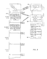
- FIG. 3 A more detailed block diagram of parts of the NVM, the ROM, RAM and CPU is represented in Fig 3.
- the NVM is represented as segmented into a plurality of blocks, in this representation, 5 full blocks with the sixth block partially represented.
- the NVM employed maybe a CMOS, such as a model MK48C021 manufactured by Mostek which operates at very fast cycle or a SEEQ model 5516AH manufactured by Seeq, which operates at a some what slower cycle.
- Each memory bank includes 2032 usable memory bytes. The bytes are represented by short bars extending from the right end of the block representing the NVM.
- each memory block includes an identical number of bytes, for example 254 bytes, with the memory bank partitioned into 8 blocks. This uses the total capability of usable bytes.
- a postage meter maintains atleast two identical accounting records of the activities of the meter.
- the records are in the form of registers such as an ascending register maintaining the dollar value of the amount of postage dispensed; a descending register, maintaining the dollar value of the postage available to be despensed against a pre-paid amount; a piece count register, maintaining a number representing the number of pieces of mail on which postage has been stamped; and a batch count register, maintaining a number representing the number of pieces of mail in a particular batch.
- registers may be used if desired, thus space is provided for the same by representation.
- the initially stored set of data in the first data memory block is referred to as the primary set of data.
- the data memory block in which the primary set of data is stored is referred to as the Primary Block.
- the initially stored set of data, which is a copy of the primary set of data, stored in the second data memory block is referred to as the secondary set of data.
- the data memory block in which the secondary set of data is stored is referred to as the Secondary Block.
- the first memory block in the memory bank which may be a shortened block, if desired, is here represented as a full block and is used to store the address of the data memory block in which the primary set of data is stored and the address of the data memory block in which the secondary set of data is stored.
- each successive block may be identified by the number of the first byte in the block, which is essentially the address of the particular block.
- the first memory block, A may be used for block address storage thus providing predetermined addresses or locations for storing the address of the block containing the primary set of records and for the address of the block containing the secondary set of records.
- the second memory block B may be used as the initial block to store the primary set of records while block C, the third block may be used as the initial block to store the secondary set of records.
- the first memory block A, and the last memory block H are used for purposes other than storing sets of data or records, however such blocks would be capable of such storage
- Preferably Block A is used for storing the address of the block in which the primary or main set of records is being stored, i.e, the Primary Block and the address of the block in which the secondary or alternate set of records in being stored, i.e, the Secondary Block. If the primary set of records experiences an error or a malfunction occurs in the block in which such records are stored, another set of primary records will be generated in another block and the address, stored in block A, of the primary set of records will be rewritten or changed at its location in the Block Address Storage, Block A.
- the differential between consecutive block addresses may be added to the highest address of the blocks in which the sets of records are actively stored.
- an accounting program to be stored in a memory bank required 254 memory bytes and that a 2032 byte memory bank were used. Assume further that each byte in the memory bank was identified by a number in numerical sequence according to its location, from first to last in the memory bank. By segmenting the 2032 byte memory bank into memory block of 254 each, the memory bank is segmented into eight (8) memory blocks.
- the first memory block (Block A) may be identified by the number or address 1, the number or address used to identify the first byte in Block A.
- the next memory block (Block B) may be identified by the number or address 255, the number or address used to identify the first byte in Block B.
- Carrying this forward Block C may be identified by the number or address 509 while the fourth block (Block C) may be identified by the number or address 763. If, as in the preferred arrangement, Block A (or address 1 ) were used for block address storage and Block B (or address 255) were used as the block for initially storing the primary set of records and Block C (or address 509) were used as the block for initially storing the secondary set of records, the remaining blocks D, E, F, G and H may be used as reserve block. The addresses of the reserve blocks would be 763, 1017, 1271, 1525 and 1779 respectively, the block address differential being 254.
- the various registers such as ascending register, decending register, piece count register, batch count register, and any other register, which may constitute the set or records or data, may each be positioned at some desired location within a memory block such as at predetermined offsets from the address of the memory block. Any offset, however, must be less than the address differential. Assume the offset of the ascending register to be 30. The address of the primary ascending register would be 255 + 30 or 285. The address of the secondary ascending register would be 509 + 30 or 539. The offset of the descending register may be 60. Thus the address of the primary descending register would be 255 + 60 or 315 while the address of the secondary descending register would be 509 + 60 or 569. The block address plus the offset for the particular register is referred to as the Effective Address. The various predetermined offsets for the various registers are stored in the permanant memory, ROM, 92.
- Calculations may be done in the CPU, 80 and the Effective Address stored, temporally in the RAM, 83.
- Figs 4, 4a, 4b, and 4c combine to form a general flow chart of the operation of the device.
- a program for carrying out the operation set forth in the flow charts may be written and stored in the ROM.
- the routine to set up or generate a new set of registers, herein referred to as Remap may occur if an error in the stored data in one set of registers is detected or if some malfunction in one of the current memory blocks is detected.
- the said copending application teaches the use of an incrementable function code individual to each register, that is stored with both the primary register and the secondary register which identifies the progress of the operation or updating effecting the particular register.
- This function code is to determine if both registers have been similarly updated. It will be appreciated that when updating data stored in the registers, the data in the primary block or primary registers is first completely updated, then the data in the secondary block or secondary registers is updated. Since the data in the secondary registers should be a duplicate or copy of the data in the primary registers, the function codes of the respective registers should be identical at the completion of the update routine.
- step 4.1 If no uncorrectable and/or malfunction is detected normal operation continues. If, on the other hand, an error is experienced, it must be determined whether or not a reserve memory block is available for use in generating a new set of registers.
- the routine to determine whether or not a reserve block is available for use is covered by the flow chart set forth in Fig 5. It is believed that the flow chart in Fig 5 is self explanatory. This routine will determine whether or not a reserve block is available. If a reserve block is available, the available reserve block will be remapped byte-by-byte until a new primary, or secondary memory block is generated.
- two sections may be used to store corresponding data while other sections may be used a reserve memory blocks or areas.
- a new set of data may be generated from the set of correct data in the other memory block by byte-by-byte duplication of the data into the next available reserve memory block or area.
- This routine may be repeated over and over again, so long as there remains a reserve block or reserve area in which to transfer and store data in order to make a new set of registers. The carrying out of this routine may greatly extend the field life of the device in which such new memory system is employed.
- a routine can be programmed to determine whether or not a previously used and subsequently abandoned memory block is available for re-use for remapping.
- This latter procedure may further extend the field life of the device in which the present novel memory system is employed.
- the principle of the present invention may be used to reposition or re-locate a register which has sustained an error in data to another location within the same memory block without rewriting the entire set of registers stored in the block.
- Such alternate arrangement may provide for reserve memory areas within the memory block, as opposed to separate areas of reserve memory block.
- the address of the primary block and the address of the secondary block would be stored in ROM and would be permanent.
- the offsets of the various registers would be stored in the NVM block address storage and the offset of the particular register would be subject to change upon relocation of the register within the memory block. In the event an individual register were re-located within a particular memory block, the corresponding register in the other memory block would also be re-located to a corresponding location.
- the offset of the particular register would be changed in the NVM block storage.
- the preferred embodiment of the invention has been described with respect to its use in a postage meter. It will be appreciated that the novel memory system may be used in any accounting and/or inventory keeping system in which data is electronically deposited, stored and retrieved. It will also be appreciated that memory banks other than those mentioned herein may be used in practicing this invention. Although the preferred arrangement of the invention includes the partitioning of a memory bank into multiple sections for remapping, it will be apparent that a plurality of memory banks maybe used where one memory bank serves as the primary bank, to store a primary set of registers a second memory bank serves as a secondary bank, to store a secondary set of registers and additional memory banks are provided to serve as reserve memory banks for the purpose of remapping.
Abstract
Description
- The present invention relates to improved electronic memory systems and more particularly to an improved electronic memory system incorporated into electronic postage meters for the purpose of maintaining a running account of the functions performed by the postage meter, particularly the accumulated amount of postage dispensed by the postage meter.
- For the most part, postal meters on the market today are rental devices. The meters are rented by the customer and usually retained and used on the premises of the customer.
- Routine servicing of the meter, such as taking readings of the registers and/or setting postage tables is usually done in the field by Postal Service representatives or other authorized service personnel. However, when a postage meter breaks down, the down meter is returned to the owner or manufacturer and a substitute postage meter is provided to the customer. The customer renting the postage meter makes no repairs or adjustments to the meter. The customer does, however, set the postage value to be printed. Bench repairs and/or adjustments, other than routing servicing, are normally made by authorized service personnel or employees of the manufacturer authorized to make such repairs and/or adjustments.
- A system of this nature requires a substantial service organization to effect exchange of the down meter and to bench service the down meter. It is also necessary to maintain a substantial inventory of postage meters available for exchange purposes. This requires a substantial investment on the part of the organization in the postage meter rental business and is reflected in the cost of the customer for his rental of postage meter.
- The philosophy of the organization in the postage meter rental business was to provide a rugged postage meter which would withstand maltreatment by the customer without breakdown but still be easily and quickly repairable by their service personnel. This philosophy was reflected in the chamber and structure of the postage meter made for rental purposes.
- Prior postage meters were essentially mechanical and relatively limited in scope. Postage values to be printed were entered into the device by the customer and printed by the meter on a label or envelope. The postage values so printed were accounted for by use of an ascending register. The register provided a record of the amount of postage printed over the life of the meter. As postage meters became more advanced, a piece count register was added to the meter to provide information on the number of pieces of mail which were passed through and printed with postage by the meter. An additional feature, which permitted pre-payment by the customer of a desired dollar amount of postage the meter may print, brought about the use of a descending register to indicate the dollar amount of postage left to be dispensed by the meter, before expiration of the pre-paid amount.
- The data set forth in the various registers provide the customer with a reasonably full accounting of the postage actively handled by the meter for the customer. The ascending and the descending registers provide a running inventory of the dollar amount of postage already dispensed against the last pre-payment made and the dollar amount of postage available to be dispensed out of the last pre-payment or advanced payment of postage made by the customer, for the meter.
- The electronic age brought a change in postage meters in which a central processing unit (CPU), such as a micro-computer or microprocessor, provides calculation and data flow control of postage dispensed and available, in accordance with input data provided. Devices of this nature are taught and described in U.S. Patent No. 3,978,457. Coupled to the CPU may be a PROM, serving as a permanent memory, for storing program information and other information and a RAM, serving as a temporary memory, for routine storing and working data in real time in coordination with calculations and operations carried on and/or controlled by the CPU. In postage meters, where it is very important to provide permanent and/or non-destructive storage location for accounting data, such as postal funding data, for example, a nonvolatile memory (NVM) is also coupled to the CPU. NVM storage has been used successfully over other known mass data storage devices such as magnetic tape or discs, which are not as secure as NVM storage and are more expensive than NVM storage devices. The use of the NVM storage device in association with a microcomputer is disclosed in U.S. Patent 4,336,434. which describes how to avoid loss of data deposited in a memory device, when the system inadvertently loses power, by use of energy stored in capacitors to provide power to the microcomputer and NVM to enable continued operation for a short period during power loss.
- U.S. Patent 4,481,604 describes another arrangement in which battery backed, dual identical CMOS memories, which are essentially NVM devices, are used both for real time accounting registers and for permanent data storage. In the'604 patent, dual, identical battery backed CMOS memories are utilized for storing the same data in corresponding registers thus having a duplication of data in duplicate memory storage systems. The data in the respective registers is periodically compared and any difference in data is used as a non-resettable fatal error in the system, thus causing a down postage meter.
- A more advanced system data storage system for use in postage meters is taught and described in co-pending U.S. Patent Application Serial No. 718,618 Filed April 1, 1985 , assigned to the same assignee as the present patent application in which a CPU provides data flow for storage in two separate storage units, providing a main set of registers and an alternate set of registers storing corresponding data.
The said co-pending application teaches that the two separate data storage units maybe separate memory devices or may be the same memory device partitioned into two separate sections. - It has been found that the transfer of data from a CPU to an NVM is subject to various errors. Various transients that may occur can cause improper reading and/or improper writing of data. It has been known for transients to result in the writing of proper data at the wrong address. While the dual storage of data system adds integrity to data storage and the said co-pending patent application provides and economical solution to the problems in dual data storage systems by partitioning an NVM device into two separate sections or using two non-identical NVM devices so as to have a primary set of registers and a secondary set of registers for storing duplicate postage accounting data, it is seen that this technique goes far in solving the problems attendant data recovery but these advances do not lenghten substantically the field life of the postage meter.
- The more modern philosophy in the postage meter business is to keep the postage meter in the field with the objective of reducing the service burden placed on rental costs, generating better customer satisfaction and creating better customer relations.
- The present invention addresses the problem of field life of the postage meter and provides a novel improved memory system that is effectively self correcting, should a non-correctable error or malfunction occur in the NVM system which would other-wise cause the postage meter to be recalled from the field for service.
- It should be kept in mind that while the present invention is described and its use explained with respect to use in a postage meter, the utility of the present novel memory system may be extended to any inventory keeping or accounting system which employs a nonvolatile memory to store data for later recovery for inventory and/or accounting or other purposes.
- The present invention provides for the partitioning of the total usable capability of a nonvolatile memory into a plurality of segments or sections and initially using two such segments, one as a primary source of data depository and the second as a secondary source of data depository and retaining the other segments as back up or reserve segments, to be used in the event that a fatal or hard error should occur in the section or segment of the NVM that is then being used for either the primary or main depository segment or the secondary or alternate data depository segment.
- In the event that a fatal or hard error should occur in the primary data register, the data in the secondary data register will be duplicated into one of the backup or reserve segments (the third segment for example) and a new primary data depository or register will be formed.
- The duplication of data from a healthy or nondefective section of the memory bank to a backup section of memory bank will be referred to as Remapping or Remap.
- The present invention provides for the partitioning or sectioning of a nonvolatile memory bank into individual sections, each section sufficiently large enough to contain the information anticipated to be placed and/or stored in the required registers for the accounting program. If for example, the memory device used has 64 thousand (64K) usable addresses and the accounting registers in the program require one thousand (1K) addresses to receive and/or store all the anticipated information to be written therein, such memory device could be separated into 64 sections of 1K addresses each. If, on the other hand the same 64K address memory were used and the register to be filled with data require 8 thousand (8K) addresses to receive and/or store all the anticipated data to be written therein, such memory device could be separated or partitioned into 8 sections of 8K address each.
- It has been found that an accounting program for a postage meter may require as few as 254 bytes or addresses in a memory bank. Such accounting program may include depositing, at predetermined locations in the memory bank, such as at predetermined offsets from a decimal point address identifying the particular memory section or block, for example, dollar value and/or numerical value representations representing respective values for an ascending register, a descending register, a piece count register, a batch count register and any other appropriate information.
- In practicing the invention, successful results have been obtained using a CMOS memory device manufactured by Mostek, having manufacture's part number MK48C021 and a SEEQ memory device manufactured by SEEQ, having manufacturer's part number 5516AH, both memory devices being indentified as nonvolatile memory devices, having atleast 2032 usable bytes or addresses. When using such memory devices for such an accounting program the total memory bank may be partitioned into eight (8) segments or blocks of 254 bytes each. Thus, from a single memory device of the type used, eight (8) memory blocks, identical in size, with each having sufficient space for depositing and storing a desired accounting program is provided.
- If the desired program is larger or smaller than defined above or the memory bank used has more or fewer memory bytes, the memory bank may be partitioned into a more appropriate number of segments. So long as each segment has sufficient capacity to contain the desired program it is not necessary that the segments of the partitioned memory bank be identical in size or have the same quantity of bytes.
- In practicing the invention as set forth above, the first of the eight memory areas or blocks may be used for the primary or main memory and the second such area maybe used for the secondary or alternate memory. The other six memory areas, each defined by a range of addresses, may be held in reserve or held available as back up memory areas for use in event that the primary memory or the secondary memory should experience a malfunction or there should be an uncorrectable error occur in the transfer of data into either the primary memory section or the secondary memory section. If a malfunction or an uncorrectable error should occur in either the primary memory or the secondary memory the data in the memory section without error is duplicated in one of the reserve memory areas (the next available memory area) and a new memory, either primary or secondary depending upon which memory experience the malfunction or error, is generated to be used as a working alternate for the memory that malfunctioned. It will be seen that this remaping of a memory section may be done over and over again, depending on the overall memory capability or number of bytes in the memory device, the size of the memory area required for the program and how many usable memory areas maybe sectioned out of the overall memory device.
- Although other data locating systems may be used, the practice of locating a particular register on the basis of a predetermined offset for such register from the first address of the particular memory block insures that any register so located will have identical location within the block regardless of which memory block that data is directed and/or stored.
- It has also been found convenient to provide each respective byte in the total memory bank with its own individual identifying number. By using a table of sequential hexadecimal numbers, each byte or address may be individually identified and located in its sequence of location in the memory bank, from the first byte to the last byte with its order of location corresponding to the numerical value or size of the hexadecimal number assigned to the byte. Each memory block or memory section may be identified by the decimal number of the first byte in the memory block.
- The address or location of any particular register within the particular memory block may be obtained by adding the offset for the register and the memory block identifying number or location. Obviously the offset number would be limited to a range of numbers less than the differential between successive block addresses.
- When the present invention is practiced using an accounting system employing first and second sets of identical accounting registers, it has been found convenient to use the first usable memory block of the memory bank for storing the address as of the memory blocks containing the first or primary set of registers, the primary block, for example, and the second or secondary set or registers, the secondary block, for example. Thus, the address in the block address storage identifying the location of the primary block could be changed for any reason whatsoever. This can also be done as far as the secondary block address is concerned.
- The invention provides for partitioning a memory bank into multiple sections or segments or blocks, which may or may not be uniform in size. Use of two of the memory sections or blocks may be made for storing information for subsequent update and/or retrieval. The remaining unused memory blocks may be held as reserve blocks for use in the event that the blocks so used experience a malfunction or error. By depositing duplicate sets of information or data in two different memory blocks, when a malfunction is experinced in one such memory block, data in the health block, ie the block not having experienced a malfunction, may be duplicated byte-by-byte to a reserve block and a new memory block is formed. The block that experinced the malfunction is then abandoned. This process may be repeated upon the occurance of other malfunctions in subsequent or newly made memory blocks until the last reserve block has been used.
- Since some malfunctions and/or errors in data storage may result from temporary or transient conditions, re-use of previously used, subsequently abandoned memory blocks is also provided for in the event that the temporary or transient condition or conditions which caused the malfunction or error are no longer present.
- A memory block previously used for storing and/or retrieving data and, after having experienced a malfunction, thereafter abandoned, may be prepared for re-use, such as by clearing the heretofore used and abandoned memory block. Clearing may be done by driving all bytes in the block memory to some uniform state, such as zero, for example.
- The procedure outlined above provides for the partitioning of the total usable capacity of a memory bank into segments or blocks, use of two of the memory blocks for initially storing data, in duplication, the holding of the other of the partitioned memory blocks in reserve status, available for subsequent use should a malfunction occur in one of the currently used blocks, the provision of duplicating data stored in a healthy block by writing such data in a reserve block to form a replacement memory block for the block having experienced a malfunction. Also provided for is the re-use of blocks previously used which had experienced a malfunction and were subsequently abandoned. This provides for the fabrication of additional reserve blocks by clearing previously used, subsequently abandoned memory blocks so as to make such previously used and subsequently abandoned memory blocks available for re-use if such blocks are capable of being cleared for further use.
- It is an object of the present invention to provide an improved electronic memory system capable of reestablishing itself after experiencing a malfunction.
- Another object is to provide a novel use of a memory bank.
- A further object is to provide an electronic memory bank which is effectively self healing should be malfunction occur.
- These and other objects will become apparant when reading the following specification in conjunction with the accompanying drawings.
-
- Fig. 1 is a block diagram of an electronic postal meter incorporating the present invention.
- Fig. 2 is a representation of a front panel of the postal meter.
- Fig. 3 is a detailed block diagram of part of the block diagram of Fig 1.
- Fig. 4, 4a, 4b and 4c combine to form general flow diagram covering use of the invention.
- Fig. 5 is a more detailed flow diagram of a function called for in Fig. 4.
- Fig. 6 is a more detailed flow diagram of another function called for in Fig. 4.
- Referring to Fig. 1, and electronic postage meter is represented in block diagram form, A
power supply 50 is normally connected to house current, 110 AC and may convert the AC to other voltages required to operate the meter. One type of electronic postal meter system in which, the present invention maybe utilized is described in U.S. Patent Number 4,251, 874. The power supply is represented as connected to the operating device viainput lead 51.Terminal 52 includes aninput 53 and an output ordisplay 54, the front panel of which is represented in Fig 2. Theoutput 54 is represented by the read out shown as a series of squares within a rectangle,each square representing a display digit. Thebuttons 60 labeled withnumbers 1 through 0, a C for CORRECTION and a period for decimal point represent part of the input section for selecting postage amounts to be printed, for example. The sixbuttons 70 in the right side portion of the panel may be used to interrogate the meter and ask, for example, the amount of used postage(a dollar value in the ascending register); the amount of unused postage ( a dollar value in descending register); the number of pieces on which postage has been applied); (a number in the piece count register); the number of pieces posted in a particular batch ( a number in the batch count register); the value of the postage printed in the particular batch ( a dollar value in the batch value register) and the total sum of the postage printed by the meter ( dollar value of postage printed). The other twobuttons - The amount, up to ten (10) figures, punched on the
key board 60, including a decimal figure, will appear on thereadout 54. When the number or amount is deemed correct and the function button has also been pushed, such as to change the value or amount of postage to be printed, the Enter Amount button 55 may be pushed to enter the amount into the meter. A key 61 is provided to lock and unlock the meter andbuttons - Referring back to Fig 1, the central processing unit or
CPU 80 may be a microprocessor manufactured by National Semi-conductor Corporation having manufacturer's model number NSC800V. Theblock multiplex 81 represents the input and output linkage between the terminal and the CPU. AROM 82, such as an off-the-shelf component model EDH7823C-30 may be serve as a permanent memory and be programmed with an appropriate program for guiding the CPU, effectively controlling the operational steps. As discussed with respect to Fig. 3, offsets for the various registers are also stored in the ROM. ARAM 83 such an off-the-shelf component model TC 551 7BP-20 or MK48COL2-25 may serve as a temporary memory. The RAM is connected to the CPU and serves as a trip control or interlock to tell the CPU when postage has been printed by the postage printing device, represented byblock 85. The value of the postage to be printed is set by the postage set, represented byblock 86, while postage value is controlled by the CPU. The permanent, running record or account of the postage meter functions are stored in the nonvolatile memory (NVM) represented byblock 100. As more fully discussed with reference to Fig 3, the NVM serves to store the accounting functions attendant the postage meter.Block 58, Communications represents remote terminals to which the postage meter may be connected. - A more detailed block diagram of parts of the NVM, the ROM, RAM and CPU is represented in Fig 3. The NVM is represented as segmented into a plurality of blocks, in this representation, 5 full blocks with the sixth block partially represented. The NVM employed maybe a CMOS, such as a model MK48C021 manufactured by Mostek which operates at very fast cycle or a SEEQ model 5516AH manufactured by Seeq, which operates at a some what slower cycle. Each memory bank includes 2032 usable memory bytes. The bytes are represented by short bars extending from the right end of the block representing the NVM. By identifying each successive byte in numerical order, the usable memory capability can be partitioned or separated into sections or blocks each containing a predetermined number of bytes, In the present representation each memory block includes an identical number of bytes, for example 254 bytes, with the memory bank partitioned into 8 blocks. This uses the total capability of usable bytes.
- In actual practice, a postage meter maintains atleast two identical accounting records of the activities of the meter. The records are in the form of registers such as an ascending register maintaining the dollar value of the amount of postage dispensed; a descending register, maintaining the dollar value of the postage available to be despensed against a pre-paid amount; a piece count register, maintaining a number representing the number of pieces of mail on which postage has been stamped; and a batch count register, maintaining a number representing the number of pieces of mail in a particular batch. Certainly other registers may be used if desired, thus space is provided for the same by representation.
- Since duplicate sets of records or data are being kept in two separate memory blocks, the initially stored set of data in the first data memory block is referred to as the primary set of data. The data memory block in which the primary set of data is stored is referred to as the Primary Block. The initially stored set of data, which is a copy of the primary set of data, stored in the second data memory block is referred to as the secondary set of data. The data memory block in which the secondary set of data is stored is referred to as the Secondary Block. In practicing the invention the first memory block in the memory bank, which may be a shortened block, if desired, is here represented as a full block and is used to store the address of the data memory block in which the primary set of data is stored and the address of the data memory block in which the secondary set of data is stored.
- In processing or varifying the integrity of the records, it may be found that one set of records has experienced an error or malfunction. In some cases, the error or malfunction may, at the time, be an uncorrectable error or malfunction. Varification of the other set of records may show this second set of records to be correct.
- Since each byte in the usable memory bank has been given a number in sequential order, each successive block may be identified by the number of the first byte in the block, which is essentially the address of the particular block. The first memory block, A may be used for block address storage thus providing predetermined addresses or locations for storing the address of the block containing the primary set of records and for the address of the block containing the secondary set of records. The second memory block B may be used as the initial block to store the primary set of records while block C, the third block may be used as the initial block to store the secondary set of records.
- In the preferred embodiment, the first memory block A, and the last memory block H are used for purposes other than storing sets of data or records, however such blocks would be capable of such storage, Preferably Block A is used for storing the address of the block in which the primary or main set of records is being stored, i.e, the Primary Block and the address of the block in which the secondary or alternate set of records in being stored, i.e, the Secondary Block. If the primary set of records experiences an error or a malfunction occurs in the block in which such records are stored, another set of primary records will be generated in another block and the address, stored in block A, of the primary set of records will be rewritten or changed at its location in the Block Address Storage, Block A.
- In order to find an address of a Reserve Block, the differential between consecutive block addresses may be added to the highest address of the blocks in which the sets of records are actively stored.
- Assume for example, an accounting program to be stored in a memory bank required 254 memory bytes and that a 2032 byte memory bank were used. Assume further that each byte in the memory bank was identified by a number in numerical sequence according to its location, from first to last in the memory bank. By segmenting the 2032 byte memory bank into memory block of 254 each, the memory bank is segmented into eight (8) memory blocks. The first memory block (Block A) may be identified by the number or
address 1, the number or address used to identify the first byte in Block A. The next memory block (Block B) may be identified by the number or address 255, the number or address used to identify the first byte in Block B. Carrying this forward Block C may be identified by the number or address 509 while the fourth block (Block C) may be identified by the number or address 763. If, as in the preferred arrangement, Block A (or address 1 ) were used for block address storage and Block B (or address 255) were used as the block for initially storing the primary set of records and Block C (or address 509) were used as the block for initially storing the secondary set of records, the remaining blocks D, E, F, G and H may be used as reserve block. The addresses of the reserve blocks would be 763, 1017, 1271, 1525 and 1779 respectively, the block address differential being 254. When it becomes desirable to find the address of the next available reserve block, for example Block D, when the primary set of records are being stored in Block B and the secondary set of records are being stored in Block C, the address differential (254) may be added to the address of the highest numbered address of the then active blocks, i.e 509 + 254 = 763, 763 being address of Block D, the first reserve block in order of appearance. - The various registers, such as ascending register, decending register, piece count register, batch count register, and any other register, which may constitute the set or records or data, may each be positioned at some desired location within a memory block such as at predetermined offsets from the address of the memory block. Any offset, however, must be less than the address differential. Assume the offset of the ascending register to be 30. The address of the primary ascending register would be 255 + 30 or 285. The address of the secondary ascending register would be 509 + 30 or 539. The offset of the descending register may be 60. Thus the address of the primary descending register would be 255 + 60 or 315 while the address of the secondary descending register would be 509 + 60 or 569. The block address plus the offset for the particular register is referred to as the Effective Address. The various predetermined offsets for the various registers are stored in the permanant memory, ROM, 92.
- Calculations may be done in the CPU, 80 and the Effective Address stored, temporally in the RAM, 83.
- Figs 4, 4a, 4b, and 4c combine to form a general flow chart of the operation of the device. A program for carrying out the operation set forth in the flow charts may be written and stored in the ROM. The routine to set up or generate a new set of registers, herein referred to as Remap, may occur if an error in the stored data in one set of registers is detected or if some malfunction in one of the current memory blocks is detected.
- It will be appreciated by those skilled in the art that there are several ways of detecting the integrity of the data stored in the memory blocks and/or determining whether or not a malfunction has been experience by a memory block. One way to check the integrity of the data stored in the various registers is described in the said co-pending application Serial Number 718,618.
- The said copending application teaches the use of an incrementable function code individual to each register, that is stored with both the primary register and the secondary register which identifies the progress of the operation or updating effecting the particular register. One purpose of this function code is to determine if both registers have been similarly updated. It will be appreciated that when updating data stored in the registers, the data in the primary block or primary registers is first completely updated, then the data in the secondary block or secondary registers is updated. Since the data in the secondary registers should be a duplicate or copy of the data in the primary registers, the function codes of the respective registers should be identical at the completion of the update routine.
- By comparing the function code in the primary block with the function code in the secondary block it can be readily ascertained whether or not both memory blocks were subjected to the same updating. A difference in the function codes of the memory blocks may indicate an error in the data stored in one of the memory blocks.
- Other data checks, as well be familiar to those skilled in the art, may be used to determine the integrity of the duplicated data, if desired.
- The routine covered by the flow chart set forth in Figs 4, 4a, 4b and 4c is followed in the event an uncorrectable error or malfunction has occurred. This is represented by the step 4.1. If no uncorrectable and/or malfunction is detected normal operation continues. If, on the other hand, an error is experienced, it must be determined whether or not a reserve memory block is available for use in generating a new set of registers.
- The routine to determine whether or not a reserve block is available for use is covered by the flow chart set forth in Fig 5. It is believed that the flow chart in Fig 5 is self explanatory. This routine will determine whether or not a reserve block is available. If a reserve block is available, the available reserve block will be remapped byte-by-byte until a new primary, or secondary memory block is generated.
- In the event that no reserve block is available a routine is provided to determine whether or not a previously used and now abandoned memory block is available for re-use. This routine is covered by the flow chart set forth is Fig 6.
- By partitioning the memory bank into multiple sections, two sections may be used to store corresponding data while other sections may be used a reserve memory blocks or areas. When an error is found in the data stored in one memory block a new set of data may be generated from the set of correct data in the other memory block by byte-by-byte duplication of the data into the next available reserve memory block or area. This routine may be repeated over and over again, so long as there remains a reserve block or reserve area in which to transfer and store data in order to make a new set of registers. The carrying out of this routine may greatly extend the field life of the device in which such new memory system is employed.
- As is well known by those skilled in the art, some malfunctions and/or errors appear uncorrectable at the time of occurrence but the memory block experiencing the apparent malfunction or error may in fact be driven to a state of usefullness. Thus, in the event that all the reserve blocks or areas have been used for remapping and no reserve block or area is available for use for remapping, a routine can be programmed to determine whether or not a previously used and subsequently abandoned memory block is available for re-use for remapping.
- This latter procedure may further extend the field life of the device in which the present novel memory system is employed.
- In an alternate arrangement the principle of the present invention may be used to reposition or re-locate a register which has sustained an error in data to another location within the same memory block without rewriting the entire set of registers stored in the block. Such alternate arrangement may provide for reserve memory areas within the memory block, as opposed to separate areas of reserve memory block. The address of the primary block and the address of the secondary block would be stored in ROM and would be permanent. The offsets of the various registers would be stored in the NVM block address storage and the offset of the particular register would be subject to change upon relocation of the register within the memory block. In the event an individual register were re-located within a particular memory block, the corresponding register in the other memory block would also be re-located to a corresponding location. The offset of the particular register would be changed in the NVM block storage.
- The preferred embodiment of the invention has been described with respect to its use in a postage meter. It will be appreciated that the novel memory system may be used in any accounting and/or inventory keeping system in which data is electronically deposited, stored and retrieved. It will also be appreciated that memory banks other than those mentioned herein may be used in practicing this invention. Although the preferred arrangement of the invention includes the partitioning of a memory bank into multiple sections for remapping, it will be apparent that a plurality of memory banks maybe used where one memory bank serves as the primary bank, to store a primary set of registers a second memory bank serves as a secondary bank, to store a secondary set of registers and additional memory banks are provided to serve as reserve memory banks for the purpose of remapping.
- It should be understood that although the invention has been described in a preferred embodiment and several alternate embodiments have been suggested and explained, other changes and modifications will become evident to those skilled in the art once they have been made aware of the principles and concepts of the invention. It is therefore intended that the appended claims shall be construed to cover the disclosed embodiment, the alternate embodiments and all variations and modifications which may fall within the scope and spirit of the invention.
Claims (26)
Applications Claiming Priority (2)
| Application Number | Priority Date | Filing Date | Title |
|---|---|---|---|
| US809454 | 1985-12-16 | ||
| US06/809,454 US4802117A (en) | 1985-12-16 | 1985-12-16 | Method of preserving data storage in a postal meter |
Publications (3)
| Publication Number | Publication Date |
|---|---|
| EP0226205A2 true EP0226205A2 (en) | 1987-06-24 |
| EP0226205A3 EP0226205A3 (en) | 1988-01-13 |
| EP0226205B1 EP0226205B1 (en) | 1992-12-23 |
Family
ID=25201378
Family Applications (1)
| Application Number | Title | Priority Date | Filing Date |
|---|---|---|---|
| EP86117469A Revoked EP0226205B1 (en) | 1985-12-16 | 1986-12-16 | Method of relocating data in and extending life of a memory system |
Country Status (5)
| Country | Link |
|---|---|
| US (1) | US4802117A (en) |
| EP (1) | EP0226205B1 (en) |
| JP (1) | JPS62175845A (en) |
| CA (1) | CA1267225A (en) |
| DE (1) | DE3687344T2 (en) |
Cited By (5)
| Publication number | Priority date | Publication date | Assignee | Title |
|---|---|---|---|---|
| WO1989011134A1 (en) * | 1988-05-09 | 1989-11-16 | Ascom Hasler Ag | Electronic computing and storage system for franking machines |
| EP0376488A2 (en) * | 1988-12-30 | 1990-07-04 | Pitney Bowes, Inc. | EPM having an improvement in accounting update security |
| GB2273185A (en) * | 1992-12-04 | 1994-06-08 | Plessey Semiconductors Ltd | Cache lock-out |
| EP0615211A1 (en) * | 1993-03-11 | 1994-09-14 | Francotyp-Postalia GmbH | Device for storing security data |
| WO2005121972A1 (en) | 2004-06-14 | 2005-12-22 | Research In Motion Limited | Method and system for securing data utilizing redundant secure key storage |
Families Citing this family (71)
| Publication number | Priority date | Publication date | Assignee | Title |
|---|---|---|---|---|
| US4931997A (en) * | 1987-03-16 | 1990-06-05 | Hitachi Ltd. | Semiconductor memory having storage buffer to save control data during bulk erase |
| US5268319A (en) * | 1988-06-08 | 1993-12-07 | Eliyahou Harari | Highly compact EPROM and flash EEPROM devices |
| CA2003375A1 (en) * | 1988-12-30 | 1990-06-30 | Nanette Brown | Epm having an improvement in non-volatile memory organization |
| US7190617B1 (en) * | 1989-04-13 | 2007-03-13 | Sandisk Corporation | Flash EEprom system |
| US5083264A (en) * | 1989-04-24 | 1992-01-21 | Xerox Corporation | Process and apparatus for saving and restoring critical files on the disk memory of an electrostatographic reproduction machine |
| US5166936A (en) * | 1990-07-20 | 1992-11-24 | Compaq Computer Corporation | Automatic hard disk bad sector remapping |
| US5177744A (en) * | 1990-09-04 | 1993-01-05 | International Business Machines Corporation | Method and apparatus for error recovery in arrays |
| JPH04162300A (en) * | 1990-10-26 | 1992-06-05 | Nec Corp | Semiconductor memory |
| GB2251324B (en) * | 1990-12-31 | 1995-05-10 | Intel Corp | File structure for a non-volatile semiconductor memory |
| GB2251323B (en) * | 1990-12-31 | 1994-10-12 | Intel Corp | Disk emulation for a non-volatile semiconductor memory |
| US5426652A (en) * | 1991-01-08 | 1995-06-20 | The Dsp Group Inc. | Data reception technique |
| CA2067466C (en) * | 1991-05-03 | 1997-07-15 | Arno Muller | Method and apparatus for testing an nvm |
| US5276844A (en) * | 1991-08-05 | 1994-01-04 | Ascom Autelca Ltd. | Protection system for critical memory information |
| US5659744A (en) * | 1991-10-15 | 1997-08-19 | International Computers Limited | Data file store system with means for efficiently managing freeing of data blocks |
| US5878256A (en) * | 1991-10-16 | 1999-03-02 | International Business Machine Corp. | Method and apparatus for providing updated firmware in a data processing system |
| US5826075A (en) * | 1991-10-16 | 1998-10-20 | International Business Machines Corporation | Automated programmable fireware store for a personal computer system |
| US5341339A (en) * | 1992-10-30 | 1994-08-23 | Intel Corporation | Method for wear leveling in a flash EEPROM memory |
| US5416782A (en) * | 1992-10-30 | 1995-05-16 | Intel Corporation | Method and apparatus for improving data failure rate testing for memory arrays |
| US5369616A (en) * | 1992-10-30 | 1994-11-29 | Intel Corporation | Method for assuring that an erase process for a memory array has been properly completed |
| US5452311A (en) * | 1992-10-30 | 1995-09-19 | Intel Corporation | Method and apparatus to improve read reliability in semiconductor memories |
| US5341330A (en) * | 1992-10-30 | 1994-08-23 | Intel Corporation | Method for writing to a flash memory array during erase suspend intervals |
| US5740395A (en) * | 1992-10-30 | 1998-04-14 | Intel Corporation | Method and apparatus for cleaning up a solid state memory disk storing floating sector data |
| US5473753A (en) * | 1992-10-30 | 1995-12-05 | Intel Corporation | Method of managing defects in flash disk memories |
| US5471604A (en) * | 1992-10-30 | 1995-11-28 | Intel Corporation | Method for locating sector data in a memory disk by examining a plurality of headers near an initial pointer |
| US5535369A (en) * | 1992-10-30 | 1996-07-09 | Intel Corporation | Method for allocating memory in a solid state memory disk |
| US5448577A (en) * | 1992-10-30 | 1995-09-05 | Intel Corporation | Method for reliably storing non-data fields in a flash EEPROM memory array |
| US5822781A (en) * | 1992-10-30 | 1998-10-13 | Intel Corporation | Sector-based storage device emulator having variable-sized sector |
| US5337275A (en) * | 1992-10-30 | 1994-08-09 | Intel Corporation | Method for releasing space in flash EEPROM memory array to allow the storage of compressed data |
| US5357475A (en) * | 1992-10-30 | 1994-10-18 | Intel Corporation | Method for detaching sectors in a flash EEPROM memory array |
| US5479633A (en) * | 1992-10-30 | 1995-12-26 | Intel Corporation | Method of controlling clean-up of a solid state memory disk storing floating sector data |
| US5627568A (en) * | 1992-12-15 | 1997-05-06 | Texas Instruments Incorporated | Display buffer using minimum number of VRAMs |
| US5559992A (en) * | 1993-01-11 | 1996-09-24 | Ascom Autelca Ag | Apparatus and method for protecting data in a memory address range |
| US5740349A (en) * | 1993-02-19 | 1998-04-14 | Intel Corporation | Method and apparatus for reliably storing defect information in flash disk memories |
| US5586285A (en) * | 1993-02-19 | 1996-12-17 | Intel Corporation | Method and circuitry for increasing reserve memory in a solid state memory disk |
| US5581723A (en) * | 1993-02-19 | 1996-12-03 | Intel Corporation | Method and apparatus for retaining flash block structure data during erase operations in a flash EEPROM memory array |
| US5835933A (en) * | 1993-02-19 | 1998-11-10 | Intel Corporation | Method and apparatus for updating flash memory resident firmware through a standard disk drive interface |
| US5640529A (en) * | 1993-07-29 | 1997-06-17 | Intel Corporation | Method and system for performing clean-up of a solid state disk during host command execution |
| GB2283342B (en) * | 1993-10-26 | 1998-08-12 | Intel Corp | Programmable code store circuitry for a nonvolatile semiconductor memory device |
| US5682517A (en) * | 1994-06-21 | 1997-10-28 | Pitney Bowes Inc. | Method of transferring data to a memory medium in a mailing machine |
| US5765175A (en) * | 1994-08-26 | 1998-06-09 | Intel Corporation | System and method for removing deleted entries in file systems based on write-once or erase-slowly media |
| US5809558A (en) * | 1994-09-29 | 1998-09-15 | Intel Corporation | Method and data storage system for storing data in blocks without file reallocation before erasure |
| US5563828A (en) * | 1994-12-27 | 1996-10-08 | Intel Corporation | Method and apparatus for searching for data in multi-bit flash EEPROM memory arrays |
| US5668973A (en) * | 1995-04-14 | 1997-09-16 | Ascom Hasler Mailing Systems Ag | Protection system for critical memory information |
| US6157919A (en) | 1995-12-19 | 2000-12-05 | Pitney Bowes Inc. | PC-based open metering system and method |
| US6151590A (en) | 1995-12-19 | 2000-11-21 | Pitney Bowes Inc. | Network open metering system |
| US5749078A (en) * | 1996-08-23 | 1998-05-05 | Pitney Bowes Inc. | Method and apparatus for storage of accounting information in a value dispensing system |
| DE19650993A1 (en) * | 1996-11-26 | 1998-05-28 | Francotyp Postalia Gmbh | Arrangement and method for improving data security using a ring buffer |
| JP3648892B2 (en) * | 1996-12-16 | 2005-05-18 | 富士通株式会社 | Computer system |
| DE19916065A1 (en) | 1999-04-09 | 2000-10-19 | Siemens Ag | Programmable read-only memory and method for operating the read-only memory |
| US6595412B2 (en) * | 2001-05-03 | 2003-07-22 | Pitney Bowes Inc. | Method for calculating indicia for mailpieces |
| US7487316B1 (en) * | 2001-09-17 | 2009-02-03 | Rockwell Automation Technologies, Inc. | Archive and restore system and methodology for on-line edits utilizing non-volatile buffering |
| JP2003196163A (en) * | 2001-12-27 | 2003-07-11 | Denso Corp | Electronic control device |
| US20050015344A1 (en) * | 2003-06-26 | 2005-01-20 | Pitney Bowes Incorporated | Method and system for detection of tampering and verifying authenticity of a 'data capture' data from a value dispensing system |
| US9104315B2 (en) * | 2005-02-04 | 2015-08-11 | Sandisk Technologies Inc. | Systems and methods for a mass data storage system having a file-based interface to a host and a non-file-based interface to secondary storage |
| US20060184718A1 (en) * | 2005-02-16 | 2006-08-17 | Sinclair Alan W | Direct file data programming and deletion in flash memories |
| US7877539B2 (en) * | 2005-02-16 | 2011-01-25 | Sandisk Corporation | Direct data file storage in flash memories |
| US20060184719A1 (en) * | 2005-02-16 | 2006-08-17 | Sinclair Alan W | Direct data file storage implementation techniques in flash memories |
| US7480766B2 (en) * | 2005-08-03 | 2009-01-20 | Sandisk Corporation | Interfacing systems operating through a logical address space and on a direct data file basis |
| US7984084B2 (en) * | 2005-08-03 | 2011-07-19 | SanDisk Technologies, Inc. | Non-volatile memory with scheduled reclaim operations |
| US7669003B2 (en) * | 2005-08-03 | 2010-02-23 | Sandisk Corporation | Reprogrammable non-volatile memory systems with indexing of directly stored data files |
| US7949845B2 (en) * | 2005-08-03 | 2011-05-24 | Sandisk Corporation | Indexing of file data in reprogrammable non-volatile memories that directly store data files |
| US7558906B2 (en) | 2005-08-03 | 2009-07-07 | Sandisk Corporation | Methods of managing blocks in nonvolatile memory |
| US7627733B2 (en) * | 2005-08-03 | 2009-12-01 | Sandisk Corporation | Method and system for dual mode access for storage devices |
| US7552271B2 (en) | 2005-08-03 | 2009-06-23 | Sandisk Corporation | Nonvolatile memory with block management |
| US7814262B2 (en) * | 2005-10-13 | 2010-10-12 | Sandisk Corporation | Memory system storing transformed units of data in fixed sized storage blocks |
| US7529905B2 (en) * | 2005-10-13 | 2009-05-05 | Sandisk Corporation | Method of storing transformed units of data in a memory system having fixed sized storage blocks |
| US7877540B2 (en) * | 2005-12-13 | 2011-01-25 | Sandisk Corporation | Logically-addressed file storage methods |
| US7747837B2 (en) | 2005-12-21 | 2010-06-29 | Sandisk Corporation | Method and system for accessing non-volatile storage devices |
| US7769978B2 (en) * | 2005-12-21 | 2010-08-03 | Sandisk Corporation | Method and system for accessing non-volatile storage devices |
| US7793068B2 (en) | 2005-12-21 | 2010-09-07 | Sandisk Corporation | Dual mode access for non-volatile storage devices |
| US20070233868A1 (en) * | 2006-03-31 | 2007-10-04 | Tyrrell John C | System and method for intelligent provisioning of storage across a plurality of storage systems |
Citations (5)
| Publication number | Priority date | Publication date | Assignee | Title |
|---|---|---|---|---|
| US2688656A (en) * | 1949-12-02 | 1954-09-07 | Standard Telephones Cables Ltd | Means for checking recorded information |
| DE1524212A1 (en) * | 1966-01-18 | 1969-05-14 | Siemens Ag | Method for ensuring the functionality of storage units in data processing systems, especially in switching systems, e.g. Telephone systems |
| US3544777A (en) * | 1967-11-06 | 1970-12-01 | Trw Inc | Two memory self-correcting system |
| US4371754A (en) * | 1980-11-19 | 1983-02-01 | Rockwell International Corporation | Automatic fault recovery system for a multiple processor telecommunications switching control |
| US4481604A (en) * | 1980-07-09 | 1984-11-06 | Roneo Alcatel Limited | Postal meter using microcomputer scanning of encoding switches for simultaneous setting of electronic accounting & mechanical printing systems |
Family Cites Families (13)
| Publication number | Priority date | Publication date | Assignee | Title |
|---|---|---|---|---|
| GB1193287A (en) * | 1967-08-08 | 1970-05-28 | Ferranti Ltd | Improvements relating to Apparatus for Reading Magnetic Tape |
| US3866182A (en) * | 1968-10-17 | 1975-02-11 | Fujitsu Ltd | System for transferring information between memory banks |
| US3569934A (en) * | 1968-12-17 | 1971-03-09 | Petty Geophysical Eng Co | Method of detecting and correcting errors in multiplexed seismic data |
| US3668644A (en) * | 1970-02-09 | 1972-06-06 | Burroughs Corp | Failsafe memory system |
| US3835312A (en) * | 1973-03-15 | 1974-09-10 | Gte Automatic Electric Lab Inc | Recovery control circuit for central processor of digital communication system |
| US3978457A (en) * | 1974-12-23 | 1976-08-31 | Pitney-Bowes, Inc. | Microcomputerized electronic postage meter system |
| US4044337A (en) * | 1975-12-23 | 1977-08-23 | International Business Machines Corporation | Instruction retry mechanism for a data processing system |
| US4251874A (en) * | 1978-10-16 | 1981-02-17 | Pitney Bowes Inc. | Electronic postal meter system |
| DE2916840A1 (en) * | 1979-04-26 | 1980-11-06 | Postalia Gmbh | ELECTRONICALLY CONTROLLED FRANKING MACHINE |
| US4281398A (en) * | 1980-02-12 | 1981-07-28 | Mostek Corporation | Block redundancy for memory array |
| JPS59157811A (en) * | 1983-02-25 | 1984-09-07 | Nec Corp | Data interpolating circuit |
| US4531215A (en) * | 1983-06-22 | 1985-07-23 | Gte Automatic Electric Incorporated | Validity checking arrangement for extended memory mapping of external devices |
| JPS6170637A (en) * | 1984-09-11 | 1986-04-11 | インタ−ナショナル ビジネス マシ−ンズ コ−ポレ−ション | Correction of error detection due to decision by majority |
-
1985
- 1985-12-16 US US06/809,454 patent/US4802117A/en not_active Expired - Lifetime
-
1986
- 1986-12-11 CA CA000525052A patent/CA1267225A/en not_active Expired - Lifetime
- 1986-12-16 JP JP61299819A patent/JPS62175845A/en active Pending
- 1986-12-16 DE DE8686117469T patent/DE3687344T2/en not_active Revoked
- 1986-12-16 EP EP86117469A patent/EP0226205B1/en not_active Revoked
Patent Citations (5)
| Publication number | Priority date | Publication date | Assignee | Title |
|---|---|---|---|---|
| US2688656A (en) * | 1949-12-02 | 1954-09-07 | Standard Telephones Cables Ltd | Means for checking recorded information |
| DE1524212A1 (en) * | 1966-01-18 | 1969-05-14 | Siemens Ag | Method for ensuring the functionality of storage units in data processing systems, especially in switching systems, e.g. Telephone systems |
| US3544777A (en) * | 1967-11-06 | 1970-12-01 | Trw Inc | Two memory self-correcting system |
| US4481604A (en) * | 1980-07-09 | 1984-11-06 | Roneo Alcatel Limited | Postal meter using microcomputer scanning of encoding switches for simultaneous setting of electronic accounting & mechanical printing systems |
| US4371754A (en) * | 1980-11-19 | 1983-02-01 | Rockwell International Corporation | Automatic fault recovery system for a multiple processor telecommunications switching control |
Cited By (12)
| Publication number | Priority date | Publication date | Assignee | Title |
|---|---|---|---|---|
| WO1989011134A1 (en) * | 1988-05-09 | 1989-11-16 | Ascom Hasler Ag | Electronic computing and storage system for franking machines |
| EP0376488A2 (en) * | 1988-12-30 | 1990-07-04 | Pitney Bowes, Inc. | EPM having an improvement in accounting update security |
| EP0376488A3 (en) * | 1988-12-30 | 1991-11-06 | Pitney Bowes, Inc. | Epm having an improvement in accounting update security |
| GB2273185A (en) * | 1992-12-04 | 1994-06-08 | Plessey Semiconductors Ltd | Cache lock-out |
| EP0615211A1 (en) * | 1993-03-11 | 1994-09-14 | Francotyp-Postalia GmbH | Device for storing security data |
| WO2005121972A1 (en) | 2004-06-14 | 2005-12-22 | Research In Motion Limited | Method and system for securing data utilizing redundant secure key storage |
| EP1759296A1 (en) * | 2004-06-14 | 2007-03-07 | Research In Motion Limited | Method and system for securing data utilizing redundant secure key storage |
| EP1759296A4 (en) * | 2004-06-14 | 2007-06-27 | Research In Motion Ltd | Method and system for securing data utilizing redundant secure key storage |
| US7653202B2 (en) | 2004-06-14 | 2010-01-26 | Research In Motion Limited | Method and system for securing data utilizing redundant secure key storage |
| US8144866B2 (en) | 2004-06-14 | 2012-03-27 | Research In Motion Limited | Method and system for securing data utilizing redundant secure key storage |
| US8280047B2 (en) | 2004-06-14 | 2012-10-02 | Research In Motion Limited | Method and system for securing data utilizing redundant secure key storage |
| US8660269B2 (en) | 2004-06-14 | 2014-02-25 | Blackberry Limited | Method and system for securing data utilizing redundant secure key storage |
Also Published As
| Publication number | Publication date |
|---|---|
| EP0226205B1 (en) | 1992-12-23 |
| DE3687344D1 (en) | 1993-02-04 |
| CA1267225A (en) | 1990-03-27 |
| JPS62175845A (en) | 1987-08-01 |
| US4802117A (en) | 1989-01-31 |
| EP0226205A3 (en) | 1988-01-13 |
| DE3687344T2 (en) | 1993-05-13 |
Similar Documents
| Publication | Publication Date | Title |
|---|---|---|
| US4802117A (en) | Method of preserving data storage in a postal meter | |
| US4780601A (en) | Control system for franking machines | |
| KR100877030B1 (en) | Non-volatile memory and non-volatile memory data rewriting method | |
| EP0376487B1 (en) | EPM having an improvement in non-volatile storage of accounting data | |
| EP0492106B1 (en) | Endurance management for solid state files | |
| CN100385415C (en) | Maintaining erase counts in non-volatile storage systems | |
| US5021963A (en) | EPM having an improvement in accounting update security | |
| US4845632A (en) | Electonic postage meter system having arrangement for rapid storage of critical postage accounting data in plural nonvolatile memories | |
| JPS62168261A (en) | Electronic postage meter having non-volatile memory | |
| US4627016A (en) | Memory address location system for an electronic postage meter having multiple non-volatile memories | |
| US5124926A (en) | Carrier management system having accounting registers | |
| AU631580B2 (en) | Epm having an improvement in non-volatile memory organization | |
| US5444631A (en) | Franking machine with record storage facility | |
| CA1267237A (en) | Nonvolatile memory protection arrangement for electronic postage meter system having plural nonvolatile memories | |
| EP0457114B1 (en) | Postage meter system for non-volatile storage of data | |
| CA2017298C (en) | Electronic odometer | |
| EP0172573A2 (en) | Electronic postage meter having multiple non-volatile memories for storing different historical information reflecting postage transactions | |
| CA1264376A (en) | Method and apparatus for locating and displaying historical information within an electronic postage meter | |
| US4361092A (en) | Process and apparatus for time card preparation and utilization and the like | |
| EP0513607B1 (en) | Method and apparatus for testing an NVM | |
| DE3828871A1 (en) | NON-VOLATILE, ELECTRONIC COUNTERS | |
| JPS638992A (en) | Electronic cash register | |
| JPH0476649A (en) | Data recovering method in power failure in counted data processing system |
Legal Events
| Date | Code | Title | Description |
|---|---|---|---|
| PUAI | Public reference made under article 153(3) epc to a published international application that has entered the european phase |
Free format text: ORIGINAL CODE: 0009012 |
|
| AK | Designated contracting states |
Kind code of ref document: A2 Designated state(s): CH DE FR GB IT LI NL |
|
| RIN1 | Information on inventor provided before grant (corrected) |
Inventor name: MAYBRUCH, JOEL Inventor name: CHROSNY, WOJCIECH M. |
|
| PUAL | Search report despatched |
Free format text: ORIGINAL CODE: 0009013 |
|
| AK | Designated contracting states |
Kind code of ref document: A3 Designated state(s): CH DE FR GB IT LI NL |
|
| 17P | Request for examination filed |
Effective date: 19880510 |
|
| 17Q | First examination report despatched |
Effective date: 19891227 |
|
| GRAA | (expected) grant |
Free format text: ORIGINAL CODE: 0009210 |
|
| AK | Designated contracting states |
Kind code of ref document: B1 Designated state(s): CH DE FR GB IT LI NL |
|
| ITF | It: translation for a ep patent filed |
Owner name: STUDIO FERRARIO |
|
| REF | Corresponds to: |
Ref document number: 3687344 Country of ref document: DE Date of ref document: 19930204 |
|
| ET | Fr: translation filed | ||
| PLBI | Opposition filed |
Free format text: ORIGINAL CODE: 0009260 |
|
| PLBI | Opposition filed |
Free format text: ORIGINAL CODE: 0009260 |
|
| 26 | Opposition filed |
Opponent name: NEOPOST LTD Effective date: 19930920 |
|
| 26 | Opposition filed |
Opponent name: FRANCOTYP- POSTALIA GMBH Effective date: 19930922 Opponent name: NEOPOST LTD Effective date: 19930920 |
|
| NLR1 | Nl: opposition has been filed with the epo |
Opponent name: FRANCOTYP- POSTALIA GMBH Opponent name: NEOPOST LTD |
|
| PGFP | Annual fee paid to national office [announced via postgrant information from national office to epo] |
Ref country code: NL Payment date: 19941231 Year of fee payment: 9 |
|
| APAC | Appeal dossier modified |
Free format text: ORIGINAL CODE: EPIDOS NOAPO |
|
| APAA | Appeal reference recorded |
Free format text: ORIGINAL CODE: EPIDOS REFN |
|
| PLAB | Opposition data, opponent's data or that of the opponent's representative modified |
Free format text: ORIGINAL CODE: 0009299OPPO |
|
| PG25 | Lapsed in a contracting state [announced via postgrant information from national office to epo] |
Ref country code: NL Effective date: 19960701 |
|
| R26 | Opposition filed (corrected) |
Opponent name: NEOPOST LTD * 930922 FRANCOTYP-POSTALIA AKTIENGESE Effective date: 19930920 |
|
| NLV4 | Nl: lapsed or anulled due to non-payment of the annual fee |
Effective date: 19960701 |
|
| PGFP | Annual fee paid to national office [announced via postgrant information from national office to epo] |
Ref country code: FR Payment date: 19971119 Year of fee payment: 12 |
|
| PGFP | Annual fee paid to national office [announced via postgrant information from national office to epo] |
Ref country code: DE Payment date: 19971125 Year of fee payment: 12 |
|
| APAC | Appeal dossier modified |
Free format text: ORIGINAL CODE: EPIDOS NOAPO |
|
| PGFP | Annual fee paid to national office [announced via postgrant information from national office to epo] |
Ref country code: GB Payment date: 19981203 Year of fee payment: 13 |
|
| PGFP | Annual fee paid to national office [announced via postgrant information from national office to epo] |
Ref country code: CH Payment date: 19981208 Year of fee payment: 13 |
|
| RDAH | Patent revoked |
Free format text: ORIGINAL CODE: EPIDOS REVO |
|
| RDAG | Patent revoked |
Free format text: ORIGINAL CODE: 0009271 |
|
| STAA | Information on the status of an ep patent application or granted ep patent |
Free format text: STATUS: PATENT REVOKED |
|
| 27W | Patent revoked |
Effective date: 19980923 |
|
| GBPR | Gb: patent revoked under art. 102 of the ep convention designating the uk as contracting state |
Free format text: 980923 |
|
| REG | Reference to a national code |
Ref country code: CH Ref legal event code: PL |
|
| APAH | Appeal reference modified |
Free format text: ORIGINAL CODE: EPIDOSCREFNO |
|
| PLAB | Opposition data, opponent's data or that of the opponent's representative modified |
Free format text: ORIGINAL CODE: 0009299OPPO |