EP0227128A2 - Memory device including a sense amplifier - Google Patents
Memory device including a sense amplifier Download PDFInfo
- Publication number
- EP0227128A2 EP0227128A2 EP86201858A EP86201858A EP0227128A2 EP 0227128 A2 EP0227128 A2 EP 0227128A2 EP 86201858 A EP86201858 A EP 86201858A EP 86201858 A EP86201858 A EP 86201858A EP 0227128 A2 EP0227128 A2 EP 0227128A2
- Authority
- EP
- European Patent Office
- Prior art keywords
- transistor
- logic
- potential
- drain
- output
- Prior art date
- Legal status (The legal status is an assumption and is not a legal conclusion. Google has not performed a legal analysis and makes no representation as to the accuracy of the status listed.)
- Granted
Links
Images


Classifications
-
- G—PHYSICS
- G11—INFORMATION STORAGE
- G11C—STATIC STORES
- G11C7/00—Arrangements for writing information into, or reading information out from, a digital store
- G11C7/06—Sense amplifiers; Associated circuits, e.g. timing or triggering circuits
- G11C7/062—Differential amplifiers of non-latching type, e.g. comparators, long-tailed pairs
-
- G—PHYSICS
- G11—INFORMATION STORAGE
- G11C—STATIC STORES
- G11C17/00—Read-only memories programmable only once; Semi-permanent stores, e.g. manually-replaceable information cards
- G11C17/08—Read-only memories programmable only once; Semi-permanent stores, e.g. manually-replaceable information cards using semiconductor devices, e.g. bipolar elements
- G11C17/10—Read-only memories programmable only once; Semi-permanent stores, e.g. manually-replaceable information cards using semiconductor devices, e.g. bipolar elements in which contents are determined during manufacturing by a predetermined arrangement of coupling elements, e.g. mask-programmable ROM
- G11C17/12—Read-only memories programmable only once; Semi-permanent stores, e.g. manually-replaceable information cards using semiconductor devices, e.g. bipolar elements in which contents are determined during manufacturing by a predetermined arrangement of coupling elements, e.g. mask-programmable ROM using field-effect devices
-
- G—PHYSICS
- G11—INFORMATION STORAGE
- G11C—STATIC STORES
- G11C7/00—Arrangements for writing information into, or reading information out from, a digital store
- G11C7/06—Sense amplifiers; Associated circuits, e.g. timing or triggering circuits
- G11C7/065—Differential amplifiers of latching type
-
- G—PHYSICS
- G11—INFORMATION STORAGE
- G11C—STATIC STORES
- G11C7/00—Arrangements for writing information into, or reading information out from, a digital store
- G11C7/06—Sense amplifiers; Associated circuits, e.g. timing or triggering circuits
- G11C7/067—Single-ended amplifiers
Landscapes
- Read Only Memory (AREA)
- Static Random-Access Memory (AREA)
Abstract
Description
- The present invention relates to a memory device with an improved sense amplifier.
- As a memory device, semiconductor IC memories are widely used. Typical examples of this type memories are a read only memory (ROM) and a random access memory (RAM). The readout of stored data from the ROM or the RAM is performed by a sense amplifier. There is yet room for improvement on the readout speed of the stored data by a prior sense amplifier.
- Fig. 1 shows a configuration of a general semiconductor read only memory (ROM). Illustrated in the figure are a
column decoder 1, column lines - (data lines) 2, column selectingMOS transistors 3, arow decoder 4, row lines (word lines) 5,MOS transistors 6 forming memory cells each of which is driven by thecorresponding line 5, aload MOS transistor 7 for charging thelines 2, and asense amplifier 8 with an output buffer. Thetransistors transistor 7 is of the depletion type. - The operation of the ROM will be described. Firstly, a given
column selecting transistor 3 is driven by thedecoder 1 to select acorresponding data line 2 connected with thetransistor 3. Secondly, a givenword line 5 is selected by therow decoder 4. Amemory cell transistor 6 provided at cross point of theselected lines selected line 5. Theselected line 2 and a sensing point S are discharged (an ON state of the transistor 6) or charged (an OFF state of the transistor 6) in accordance with the stored data - (represented by ON or OFF state) of the selectedtransistor 6. The charging operation is performed by a power supply potential E through theload transistor 7. The stored data of theselected transistor 6 corresponds to a potential of theselected line 2. Thesense amplifier 8 connected to the sensing point S senses the potential of theselected line 2. The stored data sensed by theamplifier 8 is read out to exterior through the output buffer in theamplifier 8. - The stored data of the
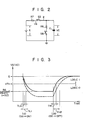
memory cell transistor 6 is determined depending on whether or not a drain (or a source) of thetransistor 6 is connected to thedata line 2. Assume now that thedecoders specific transistor 6 with its drain connected to thedata line 2. On this assumption, the charge stored in the capacitances of theselected line 2 and the sensing point S are discharged by way of a drain-source path of the selectedtransistor 6. When aselected transistor 6 with the drain unconnected to the data line 2 (in a cut-off state) is selected, theselected line 2 and the sensing point S are charged by the potential E via thetransistor 7. Thesense amplifier 8 detects either of two states of thedata line 2, i.e. charged or discharged state of thedata line 2, and outputs either logic 0 orlogic 1, which is the stored data. - Fig. 2 shows a simple equivalent circuit for illustrating the charge and discharge of one
data line 2 shown in Fig. 1. In Fig. 2, resistance R7 represents an internal resistance of theload transistor 7. Resistance R6 is representative of a conduction resistance of thememory cell transistor 6. The symbols R6 and R7 are also used to indicate equivalent resistors for providing the corresponding resistances. Switches S3 and S6 represent ON and OFF functions of thetransistors data line 2 and the sensing point S. In this example, the conduction resistance of thetransistor 3 is much smaller than the resistance R7 and therefore is neglected. Alternately, this may be considered that the resistance R7 includes the conduction resistance of thetransistor 3. - Fig. 3 shows time varying curves of a charged voltage VC or a sense potential VS of the capacitance C shown in Fig. 2. Before time t10, the switch S3 is ON, while the switch S6 is OFF, and the
line 2 is charged up to the power supply potential E. At time t10, when amemory cell transistor 6 having the stored data of logic 0 is selected by therow decoder 4, the switch S6 is ON. Then, theline 2 is discharged to a divided potential {R6/(R6 + R7)} E, or a minimum potential Ed, by the resistances R6 and R7. When, at a time t20, a memory cell transistor with its stored data oflogic 1 is selected, the switch S6 is OFF. Then, theline 2 is charged up to the maximum potential E. - A threshold level VTH for distinguishing logic 0 from
logic 1 and vice versa is set midway between the potentials E and Ed. The stored data "logic 0" is sensed when the sense potential VS is less than the level VTH. The stored data "logic 1 " is sensed when the sense potential VS is more than the level VTH. Accordingly, the read out time of the logic 0 is TL1, and the read out time of thelogic 1 is TH1. - In Fig. 3, the resistance R7 of a broken curve plotted is larger than that of a solid curve. As the resistance R7 is larger, the minimum potential Ed is lower and the read out time TL2 of the logic 0 is shorter (TL2 < TL1). When the resistance R7 becomes larger, however, a time constant C x R7 of the resistance R7 and the capacitance C is larger, so that the read out time TH2 of the
logic 1 becomes longer (TH2 > TH1). Conversely, when the resistance R7 is made small in order to shorten the read out time TH2, the read out time TL2 is elongated. If both the resistances R6 and R7 are made small, both the read out times TL and TH can be shorter, but there is limit in making the resistance R6 small. - Generally, in a semiconductor memory device, particularly a ROM, a transistor with the shortest possible channel length and width is used for each memory cell in order to make the chip size small as possible. To reduce the resistance R6 as mentioned above results in enlarging the channel width of the
transistor 6. Therefore, the memory size and hence the chip size are also made large. It is for this reason that the reduction of the resistance R6 if essentially restrictive. As a result of the progress of the integrating technology in the microelectronics, the transistor size is further smaller, while a memory capacity of the semiconductor memory is increased. Accordingly, the number of transistors connected to onedata line 2 is correspondingly increased, resulting in the increase of a capacity of thedata line 2. Consequently, the ratio a charge/di- scharge time of thedata line 2 to the total read out time is increased (address data inputted to the memory data is read out from the output buffer 8). In the case of Fig. 2, this is equivalent to the increase of the capacitance C. Accordingly, it is impossible actually to make both the read out times TL and TH small, and therefore, the selection of the read out times TL and TH must be a compromise between both the times. - The read out times TL and TH can be changed by adjusting the threshold level VTH. Resorting to even this method, a contradictive interrelation between the shortenings of the time TL and the time TH must be encountered. When the level VTH is set high, the time TL can be made short, but the time TH is long. Conversely, when the level VTH is set low, the time TH can be made short, though the time TL is long. Therefore, it is impossible to make short both the read out times TL and TH, whatever the threshold VTH is selected at any level
- For the background reasons, the present invention has an object to provide a memory device with a sense amplifier capable of shortening a read out time of stored data.
- According to the invention, there is provided a memory device comprising:
- memory cells for storing given data;
- a data line coupled to said memory cells for transferring data stored in said memory cells;
- a decoder coupled to said memory cells for selecting one of said memory cells to electrically relate the selected memory cell with said data line, the potential of said data line being changed with the stored data of said selected memory cell; and a sense amplifier coupled to said data line for sensing the stored data of said selected memory cell and providing a read out output corresponding
- to the sensed stored data;
- said sense amplifier including;
- a sensor means responsive to a first threshold level and a second threshold level for providing said read out output such that, when the data line potential departs from the first threshold level said sensor means provides a read out output representing first stored data, and when the data line potential reaches the second threshold level, said sensor means provides a read out output representing a second stored data, characterised in that said sensor means includes
- a first transistor whose gate receives said data line potential;
- a second transistor whose gate and source are respectively connected to the drain and source of said first transistor, and whose drain provides said read out output;
- first impedance means connected between the source of said first transistor and first power supply potential;
- second impedance means connected between the drain of said first transistor and a second power supply potential; and
- third impedance means connected between the drain of said second transistor and said second power supply potential;
- in which a source potential of said first transistor represents two potentials, one of which depends on the resistance ratio of said first and second impedance means and corresponds to said first threshold level, and the other of which depends on the resistance ratio of said first and third impedacne means and corresponds to said second threshold level.
- Embodiments of the invention will now be described, by way of example, with reference to the accompanying drawings, in which:
- Fig. 1 shows a configuration of a general ROM;
- Fig. 2 shows a simple equivalent circuit for illustrating the charge and discharge of one data line of the ROM shown in Fig. 1;
- Fig. 3 shows a variation of the charge and discharge to and from a capacitance C shown in Fig. 2 with respect to time;
- Fig. 4 shows a general configuration of a ROM including a sense amplifier.
- Fig. 5 shows an embodiment of a circuitry of the sense amplifier shown in Fig. 4;
- Figs. 6 and 6A to 6G are timing diagrams showing useful in explaining the operation of the circuitry shown in Fig. 5;
- Fig. 7 shows a circuit diagram of a sense amplifier which is suitable for a static RAM;
- Figs. 8A to 8C are timing diagrams useful in explaining the operation of the circuitry shown in fig. 7;
- Fig. 9 is a circuit arrangement of a modification of the sense amplifier shown in Fig. 4;
- Figs. 10A to 10E are timing diagrams illustrating a sequence of signals in the operation of the circuitry shown in Fig. 9;
- Fig. 11 is a circuit arrangement of a modification of Fig; 9;
- Fig. 12 is a circuit arrangement of another example of the circuitry of each of the comparators shown in fig. 4;
- Fig. 13 diagrammatically shows a circuitry of a logic circuit connected to the comparators shown in Fig. 5 or Fig. 12;
- Figs. 14A to 141 are a series of timing diagrams for illustrating the operation of the sense amplifier shown in Figs. 12 and 13;
- Fig. 15 illustrates a circuit arrangement of a modification of Fig. 13;
- Figs. 16A to 161 are a series of timing diagrams for illustrating the operation of the circuitry shown in Fig. 15;
- Fig. 17 illustrates a circuit arrangement of another modification of the logic circuit in Fig. 13;
- Figs. 18A to 18G are a set of timing chart for illustrating the operation of the circuitry shown in Fig. 17; and
- Fig. 19 illustrates a circuit arrangement of an embodiment of the sense amplifier shown in Fig 4, of the invention.
- Before proceeding with the description of the embodiments of the invention, it will expressly be understood that like reference symbols are used to designate like portions throughout the drawings for simplicity of illustration and that the components designated by like reference symbols may easily be replaced with each other or one another with minor change thereof by a skilled person in the art. An embodiment of a memory device according to the invention will be described.
- Referring to Fig. 4, there is shown a sense amplifier. Stored data of a
memory cell transistor 6 corresponds to charged voltages VC of adata line 2. The voltage VC is transmitted, as a sense potential VS, to a sensing point S via aMOS transistor 3 selected by acolumn decoder 1. The potential VS is applied to afirst comparator 20 and asecond comparator 30. Thecomparator 20 with a first threshold level VH produces a first comparison output a which is logic 0 when VS < VH. Thecomparator 30 with a second threshold level VL produces a second comparison output b which islogic 1 when VS > VL. The outputs a and b are inputted to alogic circuit 40. Thecircuit 40 produces an output e which becomes logic 0 immediately after the potential VS goes less than the level VH, and becomeslogic 1 immediately after the potential VS goes more than the level VL. The output e is read out of the memory device as read out data to exterior by way of anoutput buffer 12. - Fig. 5 shows a detailed circuit diagram of the
sense amplifier 10 shown in Fig. 4. The sense potential VS is applied to a gate of a depletionmode MOS transistor 22. A drain of thetransistor 22 is coupled with the power supply potential E. A source of thetransistor 22 is connected with a drain of an enhancementmode MOS transistor 26 and a gate of an enhancementmode MOS transistor 28. A gate of thetransistor 26 and a drain of thetransistor 28 are connected with a source of a depletionmode MOS transistor 24. Sources of thetransistors transistor 24 is couple with the potential E. A gate of thetransistor 24 receives the first threshold level VH. The maximum potential E is used here as the level VH. Thetransistors transistors 22 to 28 are designed so thattransistor 26 is turned OFF when VS ≥ VH, while turned ON when VS < VH. - The
transistors 22 to 28 form thefirst comparator 20. The first comparison output a is derived from the drain of thetransistor 26. - The second threshold level VL is obtained from a source of a depletion
mode MOS transistor 52 in avoltage divider 50. A drain of thetransistor 52 is connected to the power supply potential E. A source and a gate of thetransistor 52 is coupled with a drain of an enhancementmode MOS transistor 54. A source of thetransistor 54 is connected to a drain of an enhancementmode MOS transistor 56. A source of thetransistor 56 is grounded. Gates of thetransistors - The
transistors transistors transistors transistors - The sense potential VS is also applied to a gate of a depletion
mode MOS transistor 32. A drain of thetransistor 32 is coupled with the power supply potential E. A source of thetransistor 32 is connected to a drain of an enhancementmode MOS transistor 36 and a gate of an enhancementmode MOS transistor 38. A gate of thetransistor 36 and a drain of thetransistor 38 are connected with a source of a depletionmode MOS transistor 34. Sources of thetransistors transistor 34 is connected to the potential E, and its gate is supplied with the second threshold level VL. The minimum potential Ed is used as the level VL here. Pattern sizes of thetransistors 32 to 38 are so set that thetransistor 36 is turned OFF when VS > VL, and thetransistor 36 is turned ON whenVS 5 VL. - The
transistors 32 to 38 make up thesecond comparator 30. This arrangement is the same as that of saidfirst comparator 20. The second comparison output b is derived from a drain of thetransistor 36. - The first comparison output a is applied to the first input of a NOR
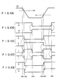
gate 42. The second comparison output b is applied to the first input of a NORgate 44. A NOR output c of thegate 42 and a NOR output d of thegate 44 are applied to the first and second inputs of a NORgate 46, respectively. A NOR output e of thegate 46 is inputted to adelay circuit 60. Thecircuit 60 includes integration circuits of two stages. Each of the integration circuits is comprised of an inverter and a CR low pass filter. A delayed output f outputted from thecircuit 60 is applied to the second input of thegate 44. The output f is inverted into an inverted output g through aninverter 48. The output g is applied to the second input of thegate 42. - Figs. 6 and 6A to 6G illustrate the operation of the circuitry of the
sense amplifier 10 shown in Fig. 5. - In Fig. 6, the first threshold level VH is illustrated lower than the maximum potential E, while the second threshold level VL is illustrated higher than the minimum potential Ed, for a better understanding, and all the MOS transistors are of the N channel type. It is evident that the levels VH and VL are actually set at these levels. Assume that a
memory cell transistor 6 of which the stored data islogic 1 is selected, before time t10. This corresponds to a state that the transistor S6 is OFF in Fig. 2. Also in this case, the sensing point S is charged up to the power supply potential E, so that the sense potential VS is equal to the power supply potential E (Fig. 6). At time t10, when atransistor 6 with the stored data of logic 0 is selected, thedata line 2 is discharged through the selectedtransistor 6. This state corresponds to a state that the transistor S6 is ON in Fig. 2. When thetransistor 6 is turned ON, the charges stored in the capacitance C of thedata line 2 is discharged through the conduction resistance R6 of thetransistor 6. In the course of the discharge, the sense potential VS substantially exponentially attenuates from the maximum potential E toward the minimum potential Ed. - At time t12, when the sense potential VS is less than the first threshold level VH, VS < VH (-E), the
transistor 26 in thefirst comparator 20 is turned ON and the output a of thecomparator 20 becomes logic 0 (Fig. 6A). When the output a becomes logic 0, the NOR output c is logic 1 (Fig. 6C) and the NOR output e is logic 0 (Fig. 6E). When the sense potential VS is equal to or less than second threshold voltage VL,VS 5 VL (- Ed) at time t14, thetransistor 36 in thesecond comparator 30 is turned ON. Upon the turning on of thetransistor 36, the output b becomes logic 0 (Fig. 68).. - The level change from
logic 1 to logic 0 of the output e is delayed by a given time period (t12 to t16) by thedelay circuit 60. At time t16, the delayed output f becomes logic 0 (Fig. 6F) and the inverted output g becomes logic 1 (Fig. 6G). With thislogic 1, the NOR output c returns in the level to logic 0 (Fig. 6C). At time t16, the output b has a logic 0 (Fig. 6B). Accordingly, the logic 0 of the output f causes the output d to have a logic 1 (Fig. 6D). After time t16, the output c becomes logic 0, while the output d becomeslogic 1. The output c changed delayed behind the output d by the signal passage time of theinverter 48. Therefore, the output e keeps its level at logic 0. - At time t20, when the
transistor 6 with alogic 1 as the stored data is selected, the charging operation for thedata line 2 starts. The sense potential VS substantially exponentially rises from the minimum potential Ed toward the maximum potential E (Fig. 6). - At time t22, when VS > VL (Fig. 6), the
transistor 36 in thecomparator 30 is turned OFF and the output b becomes logic 1 (Fig. 6B). When the output b becomeslogic 1, the NOR output d is logic 0 (Fig. 6D). At this time, the output c has a logic 0 (Fig. 6C), so that the NOR output e becomes logic 1 (Fig. 6E). At time t24, when VS 2: VH, thetransistor 26 of thecomparator 20 is turned OFF and the output ais at a logic 1 (Fig. 6A). At time t24, the output g is alogic 1 and hence the NOR output c keeps its logic 0. - The level changing operation from logic 0 to
logic 1 at the output e at time t22 is delayed by a given time period (t22 to t26) by thecircuit 60. At time t26, the delayed output f is logic 1 (Fig. 6F) and the inverted output g is logic 0 (Fig. 6G). At time t26, the output a is logic 1 (Fig. 6A), so that the NOR output c remains its logic 0 (Fig. 6C). At time t26, the output b is alsologic 1, so that the NOR output d remains its logic 0 (Fig. 6D). Accordingly, also at time t26, the NOR output e keeps itslogic 1 level (fig. 6E). The operation after time t26 is a repeat of the operation during the time period from time t10 to time t26. - The stored data in the memory cells are read out as the output e. When the stored data is logic 0, the output e is also logic 0, while when the stored data is
logic 1, the output e islogic 1. - The delay time in the
delay circuit 60 is selected so as to satisfy the following relations. - (t14-t12)≦(t16-t12)
- (t24 -t22) ≤ (t26 -t22)
- Figs. 6 and 6E shows the following facts.
- 1) The read out time TL is extremely short, which ranges from an instant (t10) that the memory cell with the logic 0 data is selected till the logic 0 data is read out (t12)..
- 2) The read out time TH is also extremely short, which ranges from an instant (t20) that the memory cell of
logic 1 is selected till thelogic 1 is read out (t22). Consequently, ROMs, static RAMs or the like of which the data read out speed is extremely high can be fabricated by using the sense amplifier according to the present invention. - Incidentally, the
transistors divider 50 are not necessarily in an ever-ON state but may be turned ON when the comparison is made by a signal synchronized with the operation timing of thedecoder 1. - Fig. 7 shows a circuit arrangement of a sense amplifier which is well adaptable for a static RAM. The potential VS on a data line is inputted to a
delay circuit 60. A delayed output h of thecircuit 60 is level-inverted to an inverted output h by aninverter 62. The potential VS is applied to gates of enhancementmode MOS transistors transistors mode MOS transistor 74. - A drain of the
transistor 74 is connected with a positive supply voltage VD. The voltage VD correspond to the potential E of Fig. 5. A source of thetransistor 70 is coupled with a drain of an enhancementmode MOS transistor 76. A source of thetransistor 72 is connected to a drain of an enhancementmode MOS transistor 78. A gate of thetransistor 76 is connected with the voltage VD and a gate of thetransistor 78 is connected to the output of theinverter 62. - A potential
VS of an inverted data line is applied to gates of enhancementmode MOS transistors transistors mode MOS transistor 84. A drain of thetransistor 84 is connected with the voltage VD. A source of thetransistor 80 is connected to a drain of an enhancementmode MOS transistor 86. A source of thetransistor 82 is coupled with a drain of an enhancementmode MOS transistor 88. A gate of thetransistor 86 is connected to the voltage VD, and a gate of thetransistor 88 is coupled with the output of thecircuit 60. Sources of thetransistors mode MOS transistor 90. A gate and a source of thetransistor 90 are connected together to another supply voltage VE corresponding to the ground potential in Fig. 5. - The
transistors 70 to 78 and thetransistors 80 to 88 make up adifferential amplifier 100 having atransistor 90 as a common impedance. When thetransistor 78 is turned ON and thetransistor 88 is turned OFF, the transconductance (gm) of thetransistors transistor 80 is low. On the other hand, when thetransistor 78 is OFF and thetransistor 88 is turned ON, the transconductance of thetransistors transistor 70 is low. A difference between those transconductances (gm) puts the input level balance of thedifferential amplifier 100 into disorder. This is a key to the circuit of Fig. 7. - Figs. 8A to 8C graphically illustrate the operation of the Fig. 7 circuit. Before time t30, the sense potential VS, the output h, and output e are all
logic 1, while the outputsVS ,h and a are all logic 0. At this time, thetransistor 70 is turned ON, while thetransistors transistor 70 is a low gm, and thetransistors - At time t30, when the memory cell of logic 0 is selected, the potential VS starts to fall, while the potential V S starts to rise. If there is no difference among those gm, the outputs e and e of the
differential amplifier 100 are not level-inverted until time t34 when VS <VS . However, the. level inversion in fact takes place at the outputs e and e even when VS >V-S , since thetransistors transistors transistor 70 is turned OFF. Then, the output e is logic 0 and the output e is logic 1 (Fig. 8C). - Following the level inversion of the potential VS, at time t36 after time lapses from t30 to t36, the delayed output h is logic 0 and the inverted output h is logic 1 (Fig. 8B). At time t36, when the outputs hand t are logic 0 and
logic 1, respectively, thetransistor 88 is turned OFF. Upon this, thetransistor 82 is also cut off to zero the drain current of thetransistor 82. Then, the voltage drop by thetransistor 84 becomes small, so that the potential of the output e slightly riese (Fig. 8C). Because of a slight amount of the potential rise, the output e yet remains logic 0. At time t36, thetransistors e keeps its state. - When the
differential amplifier 100 is of the non-cut-off type, thetransistors logic 1 state of the output n turns ON thetransistor 78. As a result, the voltage drop by thetransistor 74 increases, so that the potential of the output 9 slightly falls (as indicated by a broken line during the time period t36 to t40 in Fig. 8C). However, since the potential drop is slight, the output W keeps thelogic 1 level. In this case, thetransistors - At time t40, when a memory cell of
logic 1 is selected, the potential starts to rise, but the potential VS starts to-drop. If the gm's of the transistors are equal to one another, the outputs e and are not level-inverted until time t44 when VS >VS . At time t40, however, thetransistor 78 is turned ON and thetransistor 88 is turned OFF. Accordingly, thetransistors transistor 80 has a low gm. For this reason, the level inversion takes place even if VS < V S . At time t42, when VS > VL holds (Fig. 8A), thetransistors transistor 80 is turned OFF. As a result, the output e is logic 0 and the output e is logic 1 (Fig. 8C). - At time t46 after a given period of time (t40 to t46) from the level inversion of the potential VS, the outputs h and
h arelogic 1 and logic 0, respectively (Fig. 88). Then, thetransistor 78 is turned OFF and the potential of the output e slightly rises (Fig. 8C). After time t46, the circuit state returns to that before time t30. If thetransistors logic 1 state. - In Fig 7, if no
transistors logic 1 of the output e. As seen from Fig. 8, if the level VH is set much closer to the maximum level of the potential VS, the read out time TL for the logic 0 is extremely short. Similarly, if the level VL is set much closer to the minimum level of the potential VS, the read out time TH forlogic 1 is considerably short. In other words, a memory device at a high read out speed can be realized without speeding up the change of the potential VS. - If a plurality of transistors connected in parallel are used for the
transistor 82, thetransistor 82 has a higher gm than thetransistor 70, resulting in setting the level VH high. If thetransistor 72 is substituted by a plurality of transistors parallel connected, its gm is higher than that of thetransistor 80. The high gm may also be obtained by increasing the sizes of thetransistors transistor 82 may be set lower than that of thetransistor 70, and the threshold voltage of thetransistor 72 may be set lower than that of thetransistor 80. - Fig. 9 shows an arrangement of a modification of the
sense amplifier 10 shown in Fig. 4. A single comparator is used here, and either of two levels VH and VL is used as its comparison level. To be more specific, the first threshold level VH is used for the read out of logic 0, and the second threshold level VL is used for the read out oflogic 1. - The sense potential VS is applied to a gate of an enhancement
mode MOS transistor 104 by way of a drain-source path of an enhancementmode MOS transistor 102. A gate of thetransistor 104 is connected with a positive supply voltage VD via a source-drain path of a depletionmode MOS transistor 106. A gate of thetransistor 106 is coupled with its source. A drain of thetransistor 104 is connected with a gate and a source of a depletionmode MOS transistor 108. A drain of thetransistor 108 is connected to the voltage VD. A source of thetransistor 104 is connected with a drain of an enhancementmode MOS transistor 110. A gate of thetransistor 110 is connected to the voltage VD through a source-drain path of a depletionmode MOS transistor 112 whose gate is coupled with its source. A gate of thetransistor 110 receives the potential VS by way of a drain-source path of an enhancementmode MOS transistor 114. - A source of the
transistor 110 is connected with a drain of a depletionmode MOS transistor 116. A gate and a source of thetransistor 116 are coupled with another supply voltage VE through a drain-source path of an enhancementmode MOS transistor 118. The voltage VE may be the ground level. A gate of thetransistor 118 receives a chip enable signal CE. The signal CE becomeslogic 1 when its memory chip is in an active state. When the signal CE is logic 0, circuit elements in the chip are powered off to prevent a power dissipation. - A drain of the
transistor 116 is connected to a source of an enhancementmode MOS transistor 120. A gate of thetransistor 120 is connected with the voltage VD via a source-drain path of a depletionmode MOS transistor 122. A gate of thetransistor 122 is connected with its source. A drain of thetransistor 120 is coupled with a source of an enhancementmode MOS transistor 124. A drain of thetransistor 124 is connected to a gate and a source of a depletionmode MOS transistor 126. A gate of thetransistor 124 is connected with a gate and a source of a depletionmode MOS transistor 128. Drains of thetransistors - A first threshold level VH is applied to a gate of the
transistor 124 via a drain-source path of an enhancementmode MOS transistor 130. A gate of thetransistor 120 is supplied with a second threshold level VL by way of a drain-source path of an enhancementmode MOS transistor 132. - The level VH is obtained from a first
threshold level source 140. Thesource 140 hasseries resistors 142 and 144 connected between the voltages VD and VE. A first divided voltage V1 which appears at a junction point of theresistors 142 and 144 is applied to a gate of an enhancementmode MOS transistor 146. A source of thetransistor 146 is connected with the voltage VE, and its drain is connected to thetransistor 130 via a drain-source path of an enhancementmode MOS transistor 148. A gate of thetransistor 148 is coupled with the voltage VD. - The level VL is obtained from a second
threshold level source 150. Thesource 150 includesseries resistors resistors mode MOS transistor 156. A source of thetransistor 156 is connected with the voltage VE and its drain is coupled with thetransistor 132 through a drain-source path of an enhancementmode MOS transistor 158. A gate of thetransistor 158 is connected to the voltage VD. - The
sources resistors transistor 156 is larger than that of thetransistor 146, if the sizes of thetransistors transistor 158 is lower than a drain potential VH of thetransistor 148. - A drain of the
transistor 104 is connected with a gate of an enhancementmode MOS transistor 160. A drain of thetransistor 124 is connected with a gate of an enhancementmode MOS transistor 162. Drains of thetransistors mode MOS transistors transistors transistor 160 is connected to each drain and gate of each of enhancementmode MOS transistors transistor 162 is respectively coupled with each gate and drain of thetransistors transistors - A signal Q which appears at a source of the
transistor 160 is applied to a gate of an enhancementmode MOS transistor 172. A source of thetransistor 172 is connected to the voltage VE by way of a drain-source path of an enhancementmode MOS transistor 174. A signal Q which appears at a source of thetransistor 162 is fed to a gate of an enhancementmode MOS transistor 176. A source of thetransistor 176 is connected with the voltage VE through a drain-source path of an enhancementmode MOS transistor 178. Drains of thetransistors mode MOS transistor 180. A drain of thetransistor 180 is connected to the voltage VD. - A signal i at a source of the
transistor 180 is inputted to aninverter 182 and a gate of an enhancementmode MOS transistor 184. An output j from theinverter 182 is applied to a gate of an enhancementmode MOS transistor 186. A signal k which appears at a junction point of thetransistors inverters transistor 184 is connected between a source of thetransistor 162 and an input terminal of theinverter 188. Thetransistor 186 is connected between the input terminal of theinverter 188 and an output terminal of theinverter 190. Thecomponents 182 to 190 form alatch circuit 192 to latch a level change of the signal Q. - The signal Q is delayed by a predetermined time by a
delay circuit 60. A delayed output A of thecircuit 60 is inverted into an inverted output B by aninverter 194. The output A is applied to the gates of thetransistors transistors - Figs. 10A to 10E graphically illustrate the operation of the
sense amplifier 10 shown in Fig. 9. Before time t50, the delayed output A islogic 1 and the inverted output B is logic 0 (Fig. 10B). Accordingly, the potential VS is applied to thetransistor 104 and the first threshold level VH is applied to thetransistor 124. Before time t50, VS > VH and thetransistor 104 is ON and thetransistor 124 is almost OFF. Accordingly, the signal Q islogic 1 and the inverted signal Q is logic 0 (Fig. 10C). - When a memory cell of logic 0 is selected at time t50, the potential VS starts to drop. When VS < VH at time t52 (Fig. 10A), a differential amplifier make up of the
transistors transistor 176 is turned OFF, and the signals i and j arelogic 1 and 0, respectively (Fig. 10D). A state of i =logic 1 turns ON thetransistor 184, while a state that j = logic 0 turns OFF thetransistor 186. Then, Q = k = e = logic 0 holds (Fig. 10E). Thus, at time t52, the stored data of logic 0 is read out as the output e. - At time t54 after the delay by the
circuit 60, the outputs A and B are level-inverted (Fig. 10B). When the output B islogic 1, thetransistor 174 is turned ON. At this time point, thetransistor 172 has been turned ON by a state of Q =logic 1, and therefore i = logic 0 and j = logic 1 (Fig. 10D). As the result of the logic state that j =logic 1, a logic state of the signals of k and e, k = e = logic 0, is latched. - After time t54, the logic states of the signals A and B are logic 0 and
logic 1, respectively (Fig. 10B). As a result, the potential VS is applied to thetransistor 110 and the second threshold level VL is applied to thetransistor 120. Before time t60, thetransistor 110 is almost turned OFF, and thetransistor 120 is turned ON. Accordingly, Q = logic 0 and a = logic 1 (Fig. 10C). - when the memory cell of
logic 1 is selected at time t60, the potential VS starts to rise. At time t62, when VS > VL (Fig. 10A), a differential amplifier comprising thetransistors logic 1 and Q = logic 0 (fig. 10C). When Q = logic 0, thetransistor 172 is turned OFF and i =logic 1 and j = logic 0 (Fig. 10D). Then, thetransistor 184 is turned ON and thetransistor 186 is turned OFF, and Q = k = e = logic 1 (Fig. 10E). Thus, at a time t62, the storeddata logic 1 is read out as the output e. - At time t64, the delayed outputs A and B are level-inverted (Fig. 10B). A logical state of the output A, A =
logic 1, turns ON thetransistor 178. Thetransistor 176 has already been turned ON by the logical state of the signal Q, Q =logic 1. Accordingly, i = logic 0 and j = logic 1 (Fig. 10D). By the j =logic 1, logical state of the signals k and e, k = e =logic 1, is latched. After time t64, the same operation as that during a period from time t50 to t64 is repeated. - Fig. 11 shows a modification of the Fig. 9 circuit. In the modification, the sense potential VS is inputted into the
delay circuit 60. The remaining construction is the same as that of the Fig. 9 circuit. A basic operation of this modification is the same as that of the Fig. 9 circuit. In Figs. 9 and 11, the threshold voltage of each of thetransistors transistors - Fig. 12 shows another example of the
comparators mode MOS transistor 200. A drain of thetransistor 200 is connected with a gate and a source of a depletion mode MOS transistor 202. A source of thetransistor 200 is connected to a drain of a depletionmode MOS transistor 204 and a source of an enhancementmode MOS transistor 206. A gate and a source of thetransistor 204 are grounded. A drain of thetransistor 206 is coupled with a gate and a source of a depletionmode MOS transistor 208. Drains of thetransistors 202 and 208 are connected to a positive supply voltage VD. A gate of thetransistor 206 receives a first threshold level VH. The level VH is derived from a first threshold level source (voltage divider) 140. - A drain of the
transistor 200 is coupled with a gate of an enhancementmode MOS transistor 210. A source of thetransistor 210 is connected with a drain and a gate of enhancementmode MOS transistors transistors transistor 212 and a drain of thetransistor 214 are connected to a source of an enhancementmode MOS transistor 216. A gate of thetransistor 216 is coupled with a drain of thetransistor 206. A source of thetransistor 210 is connected to gates of enhancementmode MOS transistors transistor 216 is connected with gates of enhancementmode MOS transistors transistors transistors transistor 220, and an inverted output d is produced from a drain of thetransistor 224. - The
transistors 200 to 224 make up thefirst comparator 20. The comparison output a islogic 1 in the condition of VS > VH. When VS < VH, the output a is logic 0. The output õ has a opposite logic level to that of the outputa . - The potential VS is also inputted to a gate of an enhancement mode MOS transistor 300. The
second comparator 30 has the same configuration as that of thefirst comparator 20. In Fig. 12, lower two digits of reference numerals represent common transistors. For example, thetransistor 200 corresponds to the transistor 300. A gate of an enhancementmode MOS transistor 306 which forms a differential amplifier, together with the transistor 300, is applied with a second threshold level VL. The level VL is derived from a secondthreshold level source 150. A second comparison output b is derived from a drain of an enhancement mode MOS transistor 320: The output b islogic 1 when VS ≧ VL, and is logic 0 when VS < VL. Further, an output b with an opposite level to that of the output b is obtained from a drain of an enhancementmode MOS transistor 324. - Fig. 13 shows an arrangement of the
logic circuit 40 connected to thecomparators circuit 40 is comprised of only NAND gates. The output a is applied to a first input of aNAND gate 400. The output b is applied to a second input of thegate 400. The output b is also applied to first inputs ofNAND gates gate 400 is inputted to first inputs ofNAND gates gate 406 receives a NANDed output m of thegate 402. A NANDed output n of thegate 406 is inputted to a second input of thegate 402. The output n is level-inverted by aninverter 410. An inverted output a of theinverter 410 is applied to a second input of thegate 404. A NANDed output p of thegate 404 is inputted to a second input of thegate 408. Thegate 408 produces a NANDed output e by NAN-Ding of the outputs t and p. The output e is applied to theoutput buffer 12 in Fig. 4. - Figs. 14A to 141 graphically illustrate the operation of the sense amplifier shown in Figs. 12 and 13. Before time t70, the memory cell with the stored data of logic 0 is selected and the potential VS is at the minimum level. At time t70, when the memory cell of
logic 1 is selected, the potential VS starts to rise. At time t72, when VS > VL holds - (Fig. 14A), the signal b is logic 1 (Fig. 14C). At this time, the signal a is still logic 0 (Fig. 14B), and therefore a state t =logic 1 is still kept (Fig. 14D). Accordingly, a logic state n = logic 0 is kept because of a logic state of the signals m and t, m = t = logic 1 (Figs. 14D to 14F). If n = logic 0, o = logic 1 (Fig. 14G). At time t72, since b =logic 1 and a =logic 1, p = logic 0 (Figs. 14C, 14G and 14H). Because of p = logic 0, the output e becomes logic 1 (Fig. 141). - At time t74, when VS > VH (Fig. 14A), a = logic 1 (Fig. 14B). Then, a = b =
logic 1 and hance t = logic 0 (Figs. 14B to 14D). As the result of t = logic 0, n =logic 1 and o = logic 0 (Figs. 14F and 14G). Since b = n =logic 1, m = logic 0 (Fig. 14E). Since o = logic 0, p = logic 1 (Fig. 14H). Even if p =logic 1 at time t74, e =logic 1 is kept (Fig. 141) since t = logic 0 at this time (Fig. 14D). - At time t80, when a memory cell with the stored data of logic 0 is selected, the potential VS starts to drop (Fig. 14A). At time t82, when VS < VH, a = logic 0 (Fig. 14B). The logic state a = logic 0 brings about t = logic 1 (Fig. 14D). A logic state t = p =
logic 1 provides e = logic 0 (Figs. 14D, 14H and 141). At time t84, when VS < VL (Fig. 14A), b = logic 0 (Fig. 14C). The logic state b = logic 0 provides m = logic 1 (Fig. 14E). A relation t = m =logic 1 holds, so that n = logic 0 and o =logic 1 hold (Figs. 14F and 14G). Even if g =logic 1, b = logic 0 is still held. Therefore, a relation p =logic 1 is kept (Fig. 14H). Accordingly, e = logic 0 is kept after time t84 (Fig. 141). - Fig. 15 shows a modification of the logic circuit shown in Fig. 13. All the gates in the modification are NOR gates. The inverted signal b of the output b is inputted to first inputs of NOR
gates 420 to 426. The output a is inputted to the second inputs of thegates gate 420 is inputted to the second input ofthe-gate 422. A NORed output r of thegate 422 is delayed by adelay circuit 60 to be a delayed output s. The output s is inputted to a third input of thegate 420 and aninverter 428. An inverted output t of theinverter 428 is inputted to a third input of thegate 424. A NORed output u of thegate 424 is inputted to a second input of thegate 426. A NORed output e of thegate 426 is applied to the output buffer 12 (Fig. 4). - Figs. 16A to 161 illustrate the operation of the circuit of Fig. 15. Before time t90, a memory cell of logic 0 is selected. When at time t90 the memory cell of
logic 1 is selected and at time t92 VS > VL holds, b = logic 0 (Fig. 16C). Then, a = b = s = logic 0 and hence q = logic 1 (Fig. 160). A logic state that b = logic 0 and q = logic 0 continues for a delay time of the NORgate 420 and a logic state that r =logic 1 takes place but instantaneously disappears, and then s = logic 0 is left. Therefore, r = s = logic 0 and t =logic 1 are kept even if b = logic 0 (Figs. 16E to 16G). Further, because t =logic 1, u = logic 0 is kept - (Fig. 16H). - At time t92, if b = logic 0 (Fig. 16C), e = logic 1 (Fig. 161) since u = logic 0 (Fig. 16H).
- At time t94, if VS > VH (Fig. 16A), a = logic 1 (Fig. 16B), and then q = logic 0 (Fig. 160). At this time, since b = logic 0, r = logic 1 (Fig. 16E). When r =
logic 1, the input potential s of theinverter 428 rises (Fig. 16F). At time t96, if the potential s exceeds the input threshold of theinverter 428, t = logic 0 (Fig. 16G). - At time t100, when a memory cell of logic 0 is selected, the potential VS starts to drop. At time t102, when VS < VH (Fig. 16A), a = logic 0 (Fig. 16B). At this time, b = t = logic 0, u =
logic 1 holds (Fig. 16H). Since u =logic 1, e = logic 0 - (Fig. 161). - At time t104, when VS < VL (Fig. 16A), b = logic 1 (Fig. 16C), and then r = logic 0 (Fig. 16E). Because of r = logic 0, the potential s starts to drop. At time t106, when the potential s falls below the input threshold of the
inverter 428, t = logic 1 - (Fig. 16G), arid u = logic 0 (Fig. 16H). Since b = logic 1 (Fig. 16C) even if u = logic 0, e = logic 0 is kept (Fig. 161). - Fig. 17 shows another modification of the
logic circuit 40. The output a is inputted to gates of enhancementmode MOS transistors mode MOS transistors transistors transistors transistors transistors mode MOS transistors transistors mode MOS transistor 438, respectively. Drains of thetransistors mode MOS transistor 458, respectively. - A source of the
transistor 438 is connected with a gate of an enhancementmode MOS transistor 440 and a gate of thetransistor 456. A source of thetransistor 440 is grounded, and its drain is connected with a gate of thetransistor 436. A drain of thetransistor 440 is connected to a gate and a source of a depletionmode MOS transistor 442. Drains of thetransistors transistor 458 is connected with a gate of an enhancementmode MOS transistor 460. A source of thetransistor 460 is grounded, and its drain is connected to a gate and a source of a depletionmode MOS transistor 462. Drains of thetransistor transistor 460. - Figs. 18A to 18G graphically illustrate the operation of the
circuit 40 shown in Fig. 17. At time t112, VS > VL (Fig. 18A) and b = logic 1 (Fig. 18C). At this time, v = logic 1 (Fig. 18D), so thattransistors e representing logic 1 of the stored data is produced (Fig. 18G). - At time t114, VS > VH and a logic state a = b =
logic 1 causes thetransistors - When VS < VH at time t122 (Fig. 18A), a = logic 0 (Fig. 18B). At this time, b = logic 1 (Fig. 18C) but v = logic 0 (Fig. 18D). Therefore,
transistors logic 1 and e = logic 0 (Figs. 18F and 18G). - At time t124, when VS < VL, a = b = logic 0 and hence v =
logic 1, and w = logic 0 (Figs. 18A to 18E). After time t124, signal states similar to those before time t112 are presented. - Fig. 19 shows an embodiment of the
sense amplifier 10 shown in Fig. 4. The sense potential VS is inputted into a gate of an enhancement or depletionmode MOS transistor 470. A drain of thetransistor 470 is connected to a gate of an enhancementmode MOS transistor 472. Sources of thetransistors transistors - The circuitry of Fig. 19 forms a hysteresis comparator with two threshold levels VH and VL. When e =
logic 1, thetransistor 470 is turned ON, while thetransistor 472 is turned OFF. This indicates a state that the stored data oflogic 1 is read out. A source potential y at this time is VD*R1/(R1 + R2). This corresponds to a first threshold level VH. When VS < VH during the course of reading out the logic 0, thetransistor 470 is turned OFF and thetransistor 472 is turned ON. Then, e = logic 0. Simultaneously, the source potential y drops to VD*R1/(R1 + R3). This dropped potential level corresponds to a second threshold level VL. When VS > VL holds during the course of reading outlogic 1, thetransistor 470 is ON and thetransistor 472 is turned OFF, and e =logic 1 outputted. The threshold levels VH and VL in Fig. 19 can properly be changed in accordance with resistances of the resistors R1 to R3 and an input threshold level of thetransistor 470. The resistor R1 may be coupled with a proper negative potential in place of ground. - It is to be understood that the present invention is not limited to the embodiments thus far described in any way. For example, the MOS transistors used may be of N channel, P channel or C-MOS type. When the P channel MOS transistors are used, the polarities of the potential are inverted for those of the N channel transistors. The selection of the channel type of the transistors used are within the scope of the invention. The transistors used are not limited to the MOS FETs. The present invention is applicable for sense amplifiers using bipolar transistors or the like, or level sensors such as CCD shift registers.
- In the embodiments as mentioned above, for storing
data 0 or 1, the drain of each MOS transistor as a memory cell may be electrically connected to or disconnected from thedata line 2. Alternately, the data storage may be realized by raising or dropping the threshold voltage of the MOS transistor of the memory cell.
The delay time is preferably short as possible, so far as the above relations are satisfied. If the above relations are satisfied, a level change point (t16 or t26) of the output f of the
Claims (2)
Applications Claiming Priority (2)
| Application Number | Priority Date | Filing Date | Title |
|---|---|---|---|
| JP55133559A JPS5856198B2 (en) | 1980-09-25 | 1980-09-25 | semiconductor storage device |
| JP133559/80 | 1980-09-25 |
Related Parent Applications (1)
| Application Number | Title | Priority Date | Filing Date |
|---|---|---|---|
| EP81304262.9 Division | 1981-09-16 |
Publications (3)
| Publication Number | Publication Date |
|---|---|
| EP0227128A2 true EP0227128A2 (en) | 1987-07-01 |
| EP0227128A3 EP0227128A3 (en) | 1987-10-28 |
| EP0227128B1 EP0227128B1 (en) | 1990-07-11 |
Family
ID=15107631
Family Applications (2)
| Application Number | Title | Priority Date | Filing Date |
|---|---|---|---|
| EP81304262A Expired EP0053428B1 (en) | 1980-09-25 | 1981-09-16 | A memory device including a sense amplifier |
| EP86201858A Expired EP0227128B1 (en) | 1980-09-25 | 1981-09-16 | Memory device including a sense amplifier |
Family Applications Before (1)
| Application Number | Title | Priority Date | Filing Date |
|---|---|---|---|
| EP81304262A Expired EP0053428B1 (en) | 1980-09-25 | 1981-09-16 | A memory device including a sense amplifier |
Country Status (4)
| Country | Link |
|---|---|
| US (1) | US4445203A (en) |
| EP (2) | EP0053428B1 (en) |
| JP (1) | JPS5856198B2 (en) |
| DE (2) | DE3176940D1 (en) |
Cited By (3)
| Publication number | Priority date | Publication date | Assignee | Title |
|---|---|---|---|---|
| EP0473127A2 (en) * | 1990-08-30 | 1992-03-04 | Kabushiki Kaisha Toshiba | Semiconductor integrated circuit |
| EP0604195A2 (en) * | 1992-12-22 | 1994-06-29 | STMicroelectronics, Inc. | Dual dynamic sense amplifiers for a memory array |
| EP0660963A1 (en) * | 1992-09-21 | 1995-07-05 | Atmel Corporation | High speed memory sense amplifier with noise reduction |
Families Citing this family (16)
| Publication number | Priority date | Publication date | Assignee | Title |
|---|---|---|---|---|
| US4435658A (en) * | 1981-02-17 | 1984-03-06 | Burroughs Corporation | Two-level threshold circuitry for large scale integrated circuit memories |
| JPS5835783A (en) * | 1981-08-24 | 1983-03-02 | Fujitsu Ltd | Write control system for semiconductor memory |
| US4488264A (en) * | 1982-06-10 | 1984-12-11 | Dshkhunian Valery | Transistor storage |
| DE3381955D1 (en) * | 1982-07-26 | 1990-11-29 | Toshiba Kawasaki Kk | SEMICONDUCTOR STORAGE SYSTEM WITH DATA TRANSMISSION AND DETECTION MEANS. |
| JPS59126315A (en) * | 1982-12-24 | 1984-07-20 | Fujitsu Ltd | Comparing circuit |
| US4636664A (en) * | 1983-01-10 | 1987-01-13 | Ncr Corporation | Current sinking responsive MOS sense amplifier |
| US4654826A (en) * | 1984-08-20 | 1987-03-31 | National Semiconductor Corporation | Single device transfer static latch |
| US4719600A (en) * | 1986-02-18 | 1988-01-12 | International Business Machines Corporation | Sense circuit for multilevel storage system |
| JPS62217493A (en) * | 1986-02-27 | 1987-09-24 | Fujitsu Ltd | Semiconductor nonvolatile memory device |
| JPS62222498A (en) * | 1986-03-10 | 1987-09-30 | Fujitsu Ltd | Sense amplifier |
| US4831284A (en) * | 1988-03-22 | 1989-05-16 | International Business Machines Corporation | Two level differential current switch MESFET logic |
| JPH0274665A (en) * | 1988-09-10 | 1990-03-14 | Katsuo Shinoda | Conveyer for spreading suit raw cloth and method for cutting the same raw cloth |
| US5023838A (en) * | 1988-12-02 | 1991-06-11 | Ncr Corporation | Random access memory device with integral logic capability |
| US5293345A (en) * | 1989-06-12 | 1994-03-08 | Kabushiki Kaisha Toshiba | Semiconductor memory device having a data detection circuit with two reference potentials |
| JP2680936B2 (en) * | 1991-02-13 | 1997-11-19 | シャープ株式会社 | Semiconductor memory device |
| US5982673A (en) * | 1997-09-30 | 1999-11-09 | Siemens Aktiengesellschaft | Secondary sense amplifier with window discriminator for self-timed operation |
Citations (2)
| Publication number | Priority date | Publication date | Assignee | Title |
|---|---|---|---|---|
| US4023122A (en) * | 1975-01-28 | 1977-05-10 | Nippon Electric Company, Ltd. | Signal generating circuit |
| JPS5479527A (en) * | 1977-12-07 | 1979-06-25 | Toshiba Corp | Voltage sense circuit |
Family Cites Families (7)
| Publication number | Priority date | Publication date | Assignee | Title |
|---|---|---|---|---|
| US3648071A (en) * | 1970-02-04 | 1972-03-07 | Nat Semiconductor Corp | High-speed mos sense amplifier |
| US3953839A (en) * | 1975-04-10 | 1976-04-27 | International Business Machines Corporation | Bit circuitry for enhance-deplete ram |
| US4094008A (en) * | 1976-06-18 | 1978-06-06 | Ncr Corporation | Alterable capacitor memory array |
| US4134151A (en) * | 1977-05-02 | 1979-01-09 | Electronic Memories & Magnetics Corporation | Single sense line memory cell |
| US4123799A (en) * | 1977-09-19 | 1978-10-31 | Motorola, Inc. | High speed IFGET sense amplifier/latch |
| JPS553210A (en) * | 1978-06-21 | 1980-01-11 | Toshiba Corp | Waveform shaping circuit |
| JPS5824874B2 (en) * | 1979-02-07 | 1983-05-24 | 富士通株式会社 | sense circuit |
-
1980
- 1980-09-25 JP JP55133559A patent/JPS5856198B2/en not_active Expired
-
1981
- 1981-09-16 EP EP81304262A patent/EP0053428B1/en not_active Expired
- 1981-09-16 EP EP86201858A patent/EP0227128B1/en not_active Expired
- 1981-09-16 DE DE8181304262T patent/DE3176940D1/en not_active Expired
- 1981-09-16 DE DE8686201858T patent/DE3177199D1/en not_active Expired - Lifetime
- 1981-09-21 US US06/304,036 patent/US4445203A/en not_active Expired - Lifetime
Patent Citations (2)
| Publication number | Priority date | Publication date | Assignee | Title |
|---|---|---|---|---|
| US4023122A (en) * | 1975-01-28 | 1977-05-10 | Nippon Electric Company, Ltd. | Signal generating circuit |
| JPS5479527A (en) * | 1977-12-07 | 1979-06-25 | Toshiba Corp | Voltage sense circuit |
Non-Patent Citations (1)
| Title |
|---|
| PATENT ABSTRACTS OF JAPAN, vol. 3, no. 102 (E-133), 29th August 1979, page 53 E 133; & JP-A-54 079 527 (TOKYO SHIBAURA DENKI K.K.) 25-06-1979 * |
Cited By (7)
| Publication number | Priority date | Publication date | Assignee | Title |
|---|---|---|---|---|
| EP0473127A2 (en) * | 1990-08-30 | 1992-03-04 | Kabushiki Kaisha Toshiba | Semiconductor integrated circuit |
| EP0473127A3 (en) * | 1990-08-30 | 1993-05-19 | Kabushiki Kaisha Toshiba | Semiconductor integrated circuit |
| EP0660963A1 (en) * | 1992-09-21 | 1995-07-05 | Atmel Corporation | High speed memory sense amplifier with noise reduction |
| EP0660963A4 (en) * | 1992-09-21 | 1995-12-06 | Atmel Corp | High speed memory sense amplifier with noise reduction. |
| EP0604195A2 (en) * | 1992-12-22 | 1994-06-29 | STMicroelectronics, Inc. | Dual dynamic sense amplifiers for a memory array |
| EP0604195A3 (en) * | 1992-12-22 | 1994-11-09 | Sgs Thomson Microelectronics | Dual dynamic sense amplifiers for a memory array. |
| US5455802A (en) * | 1992-12-22 | 1995-10-03 | Sgs-Thomson Microelectronics, Inc. | Dual dynamic sense amplifiers for a memory array |
Also Published As
| Publication number | Publication date |
|---|---|
| EP0053428A3 (en) | 1984-04-04 |
| EP0227128A3 (en) | 1987-10-28 |
| US4445203A (en) | 1984-04-24 |
| EP0227128B1 (en) | 1990-07-11 |
| EP0053428B1 (en) | 1988-11-17 |
| JPS5758297A (en) | 1982-04-07 |
| DE3176940D1 (en) | 1988-12-22 |
| JPS5856198B2 (en) | 1983-12-13 |
| EP0053428A2 (en) | 1982-06-09 |
| DE3177199D1 (en) | 1990-08-16 |
Similar Documents
| Publication | Publication Date | Title |
|---|---|---|
| EP0227128A2 (en) | Memory device including a sense amplifier | |
| US4800304A (en) | Time delay circuit for a semiconductor device | |
| US4654831A (en) | High speed CMOS current sense amplifier | |
| EP0212665B1 (en) | Sense amplifier for static memory | |
| EP0350879B1 (en) | Output buffer circuit of semiconductor integrated circuit | |
| EP0834883B1 (en) | Semiconductor nonvolatile memory device | |
| US6943603B2 (en) | Pulse generating circuit and semiconductor device provided with same | |
| EP0368328B1 (en) | Address transition detector circuit | |
| KR900003894A (en) | Integrated semiconductor circuit | |
| US4447893A (en) | Semiconductor read only memory device | |
| US4709352A (en) | MOS read-only memory systems | |
| JPH0344400B2 (en) | ||
| US5654926A (en) | Semiconductor memory device | |
| US4926379A (en) | Data read circuit for use in semiconductor memory device | |
| KR100600542B1 (en) | Semiconductor device having current auxiliary circuit for output circuit | |
| US4439697A (en) | Sense amplifier circuit | |
| US7057944B2 (en) | Semiconductor readout circuit | |
| KR20010098860A (en) | Semiconductor storage device | |
| US5204838A (en) | High speed readout circuit | |
| EP0149403A2 (en) | Sense amplifier for static MOS memory | |
| JPS5914832B2 (en) | voltage sense circuit | |
| US4787068A (en) | MOS-type memory circuit | |
| NL8800893A (en) | WRITING READING CIRCUIT. | |
| JPS5938674B2 (en) | Storage device | |
| JPH07105694A (en) | Mask rom element and mask rom using it |
Legal Events
| Date | Code | Title | Description |
|---|---|---|---|
| PUAI | Public reference made under article 153(3) epc to a published international application that has entered the european phase |
Free format text: ORIGINAL CODE: 0009012 |
|
| 17P | Request for examination filed |
Effective date: 19861031 |
|
| AC | Divisional application: reference to earlier application |
Ref document number: 53428 Country of ref document: EP |
|
| AK | Designated contracting states |
Kind code of ref document: A2 Designated state(s): DE FR GB |
|
| PUAL | Search report despatched |
Free format text: ORIGINAL CODE: 0009013 |
|
| AK | Designated contracting states |
Kind code of ref document: A3 Designated state(s): DE FR GB |
|
| 17Q | First examination report despatched |
Effective date: 19890206 |
|
| GRAA | (expected) grant |
Free format text: ORIGINAL CODE: 0009210 |
|
| AC | Divisional application: reference to earlier application |
Ref document number: 53428 Country of ref document: EP |
|
| AK | Designated contracting states |
Kind code of ref document: B1 Designated state(s): DE FR GB |
|
| REF | Corresponds to: |
Ref document number: 3177199 Country of ref document: DE Date of ref document: 19900816 |
|
| ET | Fr: translation filed | ||
| PLBE | No opposition filed within time limit |
Free format text: ORIGINAL CODE: 0009261 |
|
| STAA | Information on the status of an ep patent application or granted ep patent |
Free format text: STATUS: NO OPPOSITION FILED WITHIN TIME LIMIT |
|
| 26N | No opposition filed | ||
| PGFP | Annual fee paid to national office [announced via postgrant information from national office to epo] |
Ref country code: GB Payment date: 19970908 Year of fee payment: 17 |
|
| PGFP | Annual fee paid to national office [announced via postgrant information from national office to epo] |
Ref country code: FR Payment date: 19970909 Year of fee payment: 17 |
|
| PGFP | Annual fee paid to national office [announced via postgrant information from national office to epo] |
Ref country code: DE Payment date: 19970919 Year of fee payment: 17 |
|
| PG25 | Lapsed in a contracting state [announced via postgrant information from national office to epo] |
Ref country code: GB Free format text: LAPSE BECAUSE OF NON-PAYMENT OF DUE FEES Effective date: 19980916 |
|
| GBPC | Gb: european patent ceased through non-payment of renewal fee |
Effective date: 19980916 |
|
| PG25 | Lapsed in a contracting state [announced via postgrant information from national office to epo] |
Ref country code: FR Free format text: LAPSE BECAUSE OF NON-PAYMENT OF DUE FEES Effective date: 19990531 |
|
| PG25 | Lapsed in a contracting state [announced via postgrant information from national office to epo] |
Ref country code: DE Free format text: LAPSE BECAUSE OF NON-PAYMENT OF DUE FEES Effective date: 19990701 |
|
| REG | Reference to a national code |
Ref country code: FR Ref legal event code: ST |