EP0229692A2 - Data processing apparatus - Google Patents
Data processing apparatus Download PDFInfo
- Publication number
- EP0229692A2 EP0229692A2 EP87300118A EP87300118A EP0229692A2 EP 0229692 A2 EP0229692 A2 EP 0229692A2 EP 87300118 A EP87300118 A EP 87300118A EP 87300118 A EP87300118 A EP 87300118A EP 0229692 A2 EP0229692 A2 EP 0229692A2
- Authority
- EP
- European Patent Office
- Prior art keywords
- interrupt
- stopping
- event
- clock
- processor
- Prior art date
- Legal status (The legal status is an assumption and is not a legal conclusion. Google has not performed a legal analysis and makes no representation as to the accuracy of the status listed.)
- Granted
Links
Images


Classifications
-
- G—PHYSICS
- G06—COMPUTING; CALCULATING OR COUNTING
- G06F—ELECTRIC DIGITAL DATA PROCESSING
- G06F1/00—Details not covered by groups G06F3/00 - G06F13/00 and G06F21/00
- G06F1/26—Power supply means, e.g. regulation thereof
- G06F1/32—Means for saving power
- G06F1/3203—Power management, i.e. event-based initiation of a power-saving mode
- G06F1/3206—Monitoring of events, devices or parameters that trigger a change in power modality
- G06F1/3215—Monitoring of peripheral devices
Definitions
- This invention relates to data processing apparatus and a method for stopping a system clock in a computer, and more particularly for stopping a system clock in a battery operated computer to reduce power consumption.
- CMOS complementary metal-oxide-silicon
- the circuits need not be clocked when their usage is not required.
- the characteristics of CMOS circuits provide very low standby power consumption when they are not being clocked.
- application programs and the operating system software that are running on the data processing system must be able to stop the system clocks when the central processor is waiting for the completion of an I/O operation or for further operator input.
- U. S. Patent 3,941,989 discloses one method for reducing power consumption in calculators wherein lower duty cycle power and lower duty cycle clock pulses are supplied during the calculator display mode. While the calculator is in an execute mode, continuous power and a high rate clock are supplied. If an execute mode is not initiated within a selected time interval, the duty cycle of both the power and the clock are lowered even further than that provided during the display mode.
- U. S. Patent 4,435,761 disclose a data processing apparatus having both a data transmitting and receiving unit for transferring data, and a processing unit for processing the data. Means are provided for stopping the supply of a control clock signal while the transmission of data is in progress.
- the microprocessor supplies a signal to the electronic switch thereby keeping it in the conductive state until the software program has been fully executed.
- a similar approach is shown in U. S. Patent 4,203,153.
- U. S. Patent 4,409,665 discloses the conservation of power in a calculator having a memory utilizing CMOS circuits. Incorporation of two switched voltages and a single non-switched voltage enables power to be switched off to the calculator's logic, display interface and keystroke detect circuitry, while power is maintained to the memory. In other embodiments, multiple modes such as off mode, display only mode, process only mode, and a display and process mode are used to optimize power dissipation. The calculator powers up into the display mode until a keystroke is detected. At that time, power is supplied to the processor until completion of the processing. This power conservation is effected using a first power switching means connected to a first circuit group and to a power consumption controller, and a second power switching means connected to the power consumption controller and to a second circuit group.
- an apparatus and method are provided for disabling the clocking of a central processor in a battery operated computer during non-processing times.
- Means are provided for disabling the clocking at the conclusion of a processing operation and for enabling the clocking of the processor using interrupts from any one of a plurality of sources.
- interrupts include direct memory access (DMA) interrupts, as well as I/O interrupts which occur when an I/O device needs services.
- DMA direct memory access
- I/O interrupts invoke short routines located in either ROM or in a main application program that are used to service an I/O device.
- the I/O devices include a display, printer, diskette drives, a keyboard, and communication devices such as a modem and a RS232 communication interface, and a system timer.
- a function which provides application programs and operating system programs running on the computer system with a method to specify the stopping of system clocks and the central processor until a specified event which had been requested occurs or until an optional time-out period has expired.
- the event is defined as one that results in either a system interrupt from one of the plurality of I/O devices or from a DMA operation.
- System bus 44 provides data communication among interrupt controller 12, CPU 11 through bus control 29, sleep clock control 32, direct memory access controller 13, system RAM 15, system ROM 16, keyboard controller 17, system timer 18, diskette controller 19, real time clock 21, modem 22 and RS232 communication interface 23, display controller 14, printer interface 24, and expansion connector 36.
- Expansion connector 36 provides communication with other I/O devices not shown in Fig. 1.
- Direct memory access (DMA) controller contains both clocked and unclocked sections, i.e., some sections of controller 13 require continuous clocking while others do not.
- Sleep clock control 32 is essentially a switch mechanism.
- System clock 33 provides a clock input over line 50 to sleep clock control 32.
- sleep clock control 32 passes this clocking signal over output 40 to bus 51.
- the clocking signal is provided to CPU 11 as well as to the remainder of the devices on bus 51.
- no clocking signal is provided from output 40 of sleep clock control 32.
- a clocking signal is provided at all times over bus 53 to keyboard controller 17, system timer 18, diskette controller 19, modem 22, RS232 communication interface 23, printer interface 24, display controller 14, and expansion connector 36. These devices are continually clocked by system clock 33. It is only CPU 11, system RAM 15, DMA con-troller 13, and bus controller 29 to which the clock signal from system clock 33 is turned on and off, thereby saving power.
- Interrupt controller 12 receives interrupts from printer interface 24, modem 22, and RS232 communication interface 23, real time clock 21, diskette controller 19, system timer 18, and keyboard controller 17. An interrupt request is sent from interrupt controller 12 over line 52 to sleep clock control 32. When this occurs, sleep clock control 32 provides over output 40 a clocking signal out over bus 51. Interrupt controller 12 also provides an interrupt signal as well as a non-maskable interrupt (NMI) signal to CPU 11. Finally, whenever a direct memory access request is received by DMA controller 13, it outputs over line 60 a DMA request to sleep clock control 32. Sleep clock control 32 then provides a clocking signal over output 40 onto bus 51. This occurs whenever an I/O device requires direct memory access.
- NMI non-maskable interrupt
- Sleep clock control 32 continues to supply the clock over bus 51 until the "Wait for External Event" code executing in CPU 11 from ROM 16 issues an ARM and STOP CLOCK I/O instruction. These instructions cause data to travel over bus 44 to sleep clock control 32. Sleep clock control then stops clock output 40, causing the clock signal on bus 51 to stop. This suspends execution of CPU 11 and other associated components. If an interrupt or DMA request is received after the ARM instruction has been issued but before or during the issuance of the STOP CLOCKS instruction, the sleep clock control 32 will not honor the STOP CLOCKS instruction and the clock on bus 52 will continue to run causing the CPU 11 to continue execution after the STOP CLOCKS instruction.
- CPU 11 At a time when CPU 11 is executing an application program or an I/O task, it waits for a task to be performed by one of the I/O devices. The dispatching of such a task by the operating system running on CPU 11 is included as an example and does not form a part of the present invention and will not be discussed further hereinafter.
- CPU 11 goes through a series of determinations. In decision block 41, a determination is made as to whether or not the communication queue is empty, i.e., whether modem 22 or RS232 communication interface 23 require an operation to be performed.
- CPU 11 dispatches using its operating system the communication task which is to be performed. However, if the communication queue is empty, then a second determination is made. In this case, as shown in decision block 42, a determination is made as to whether or not the video queue is empty. Once again, if it's not, then CPU 11 dispatches a video processing task as shown in step 47. However, if the video queue is empty, then a determination is made as to whether or not the printer queue is empty. If it is not, then as shown in step 48, a printer processing test is dispatched from CPU 11. Upon the printer queue being empty, the queue of keyboard controller 17 is next checked as shown in step 45.
- CPU 11 dispatches a keyboard processing task as shown in step 49.
- CPU 11 goes into a mode where it waits for an external event.
- the "Wait for External Event" routine is then entered. It will ARM sleep clock control 32 by issuing an ARM and STOP I/O command over bus 44 which causes sleep clock control 32 to stop providing a clock on bus 51, thus suspending processing of CPU 11 after the I/O instruction.
- CPU 11 will stay unclocked until an interrupt or DMA request is received by sleep control 32, at which point clocks are again provided on bus 55. This will cause CPU 11 to resume instruction processing of the event determination routine. Since a wait for any event was requested in this case, control is returned to the top of the dispatched as shown in Figure 2.
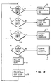
- the flow chart of Fig. 3 explains the operation of the system as it awaits an external event or until an optional time-out period has expired.
- an external event is defined as one that results in either a system interrupt or in a DMA operation, either of which causes a clocking signal to be restarted to those non-continuously clocked devices in the system.
- the computer code used to carry out the operation of Fig. 3 is contained in system ROM 16. The particular code may be called by another program residing in ROM 16 or may be called by an application running in RAM 15.
- a wait for specific event flow is shown in Figure 3.
- decision block 61 a determination is first made as to whether or not a time-out function has been requested.
- a time-out function is used only by certain ones of the I/O devices in the system. For example, diskette controller 19 requires a time-out because if either one of diskette drives 26 or 27 were to malfunction during a read or write operation, then CPU 11 could wait indefinitely for an event that will not occur due to an error.
- a time-out function is used, then if a read or write operation is not completed within the allotted time-out period, then the CPU 11 clock is restarted by timer 18 and the code in ROM indicates a time-out error to the application program or operating system, thereby allowing corrective action to be taken. Consequently, if a time-out has been requested, then as shown in step 62, a time-out counter is set in RAM 15 and a time-out requested flag is set to be active. If no time-out has been requested or the time-out counter and flag have been set, then a determination is made as to whether or not the system is waiting for any event to occur, or if a specific event is being waited for.
- the sleep clock control 32 is armed and in block 65 sleep clock control 32 stops the system clocks.
- the CPU execution will be suspended in block 65 until an external event, interrupt or DMA request occurs. At that time, CPU 11 instruction execution is resumed and control passed back to the program requesting the wait for external event.
- decision block 66 a determination is made as to whether or not the specific event being waited for will be compared with a pre-existing mask. This determination is used to compare the predetermined mask on a byte basis with the event being waited for. In other words, a predetermined byte of data describing the occurrence of a specific event, or specific events, is compared on a byte basis with the events which occur in the system. If this is the case, then as shown in step 67, the flow chart will continue to Fig. 4 which will be explained in more detail hereinafter.
- decision block 66 determines whether or not any occurring events are to be compared on a byte basis with the predetermined event which is being waited for.
- Decision block 68 makes a determination as to whether or not the occurring event will be compared on a bit by bit basis with the predetermined event upon which the system is waiting.
- the compare byte approach is useful when one specific event is being waited for, and the compare bits approach is useful when a select set of events is being waited for.
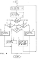
- the flow chart of Fig. 4 depicts the comparison of an incoming data request with a predetermined event mask when the two are to be compared on a byte basis.
- step 73 the sleep clock arm control of sleep control 32 is enabled. Recall that this is the first part in the two part process for stopping the system clock 33 to the non-continuously clocked devices in the system.
- step 74 the data to which the event occurrence data is to be compared on the byte basis is read from the specified location in either system RAM 15 or from the location in the specific I/O device that has been requested.
- decision block 75 a determination is made as to whether the two pieces of data are to be compared for an equal or a not equal.
- decision block 77 determines whether or not the event data is equal to the predetermined data (mask). If an equality exists, then as shown in step 79, the predetermined event has occurred and a good return code is set and the operation is carried out by the system. However, if the answer to decision block 77 is no, then a second determination is made in decision block 81 as to whether or not a time-out flag has been set, i.e., has the wait time limit expired. If the answer is yes, then in step 82 a time-out return code is set and the program requesting the wait is notified.
- step 83 the routine shown in Figure 6 is executed which stops the clock and then checks for the time limit expiration after the clock is restarted by an external event (DMA or interrupt request).
- DMA external event
- a similar operation takes place when the incoming data is compared with the predetermined mask to determine if they are not equal. This is done in decision block 76 and a no here indicates that the event, i.e., a not equal has occurred and a good return code is set and the program waiting for the event is notified of its occurrence. If the data in the mask are equal, which is not the sought after event, then the time-out flag is examined as was done previously.
- event occurrence data may be set by an I/O interrupt service routine or directly by an I/O device itself through an I/O read or direct memory access.
- the flow chart of Fig. 5 explains the operation when the event occurrence data is compared on a bit by bit basis with the predetermined event which is being waited for.
- the operation of the flow chart of Fig. 5 is identical to the operation of the flow chart of Fig. 4 except that bits are being compared rather than an entire byte. Consequently, decision block 87 functions the same as decision block 75 except that the answers depend upon whether or not the bits being compared are equal or not equal. That is, if the bits being compared in decision block 87 are equal, then decision block 89 is reached. However, if the bits being compared in decision block 87 are not equal, then decision block 88 is reached.
- step 93 performs the same function as step 79.
- step 92 performs the same function as step 78.
- the operation of decision block 91 as well as steps 94 and 95 is the same as decision block 81 and steps 82 and 83 respectively.
- Step 101 indicates that a stop clock command is issued to the stop clock circuitry within stop clock control 32. Note that if the stop clock circuitry has not been previously armed, or has been disarmed by an event already occurring, then no stopping of the clocking signal from output 40 will occur. After the sleep clock 51 has been restarted, i.e., sleep clock 32 has once again begun outputting the clocking signal over output 40 to the clocked devices in the system by either a DMA request or by an interrupt request, then decision block 102 is reached.
- step 104 a time-out flag is first set. After the time-out flag has been set in step 104, then system operation returns once again to either decision block 67 or 69.
- the flow charts of Fig. 7 and Fig. 8 explain the operation of the system while a program running on CPU 11 is waiting for a keystroke to occur or for one of diskette drives 26 or 27 to be accessed, respectively.
- the flow chart of Fig. 7 details the operation of the system of the present invention as the program running on CPU 11 awaits a keystroke from keyboard 28.
- the running program invokes a wait-for-keyboard-event function by specifying that the program wait for a compare not equal. That is, the keyboard buffer start is not equal to the keyboard buffer end, thereby signifying that keyboard data has been received. This result describes a keyboard event. Addition-ally, no time limit is set for this keyboard event to occur.
- step 112 the sleep clock control circuitry is armed but the system clock continues to be provided over output 40.
- step 114 the start and end pointers of a keyboard buffer (not shown) are compared. If the start and end pointers are not equal, then this is an indication that the awaited for keyboard data has been received and there is no longer a need to wait for a further keyboard event. Subsequently, the keystroke which has been entered is processed. However, if the pointers are equal, then as shown in step 115, the system clock output over line 51 is halted by sleep clock control 32.
- step 116 the execution by CPU 11 is stopped until either a direct memory access request or an interrupt request is presented to sleep clock control 32, which in turn resumes the outputting of the system clock over output 40 to bus 51.
- step 117 CPU execution is resumed after the receipt of an interrupt, and in step 118, the scan code of the keystroke which was just received will be put into the keyboard buffer and the end pointer of the buffer will be incremented thereby making the start and end pointer of the buffer not equal.
- step 119 indicates that execution is returned to the sleep routine, thereby rearming the sleep clock and determining that the keyboard event has occurred.
- step 121 the executing program sends commands to diskette controller 19.
- the executing program invokes a "wait for external event" routine and specifies a return operation when a diskette interrupt received flag has been set.
- a time-out period is set to cause the wait to be aborted if the event being waited for has not occurred within that time-out period.
- the stop clock control circuitry is armed, but the system clock continues to be provided over output 40 to the non-continuously clocked devices.
- decision block 124 a determination is made as to whether or not a diskette interrupt bit has been set. If the bit has been set, then this is an indication that a diskette interrupt has been received by interrupt controller 12 and so the "wait on external event" routine is exited in order to check to see if the diskette operation has been completed.
- step 129 a determination is made as to whether or not either of diskette drives 26 or 27 were the device requesting the interrupt. If so, then an interrupt handler for one of diskette drives 26 or 27 will set the diskette interrupt received bit. Finally, in step 130 after the interrupt has been handled and processed, control is returned to the wait for external event routine to determine that the event has occurred. The wait routine is then exited.
Abstract
Description
- This invention relates to data processing apparatus and a method for stopping a system clock in a computer, and more particularly for stopping a system clock in a battery operated computer to reduce power consumption.
- In the data processing environment, a large percentage of a central processor's time is spent in idle loops waiting for one or more I/O devices to complete an operation or for further input to the processor from an operator. In a system where AC power is being used to provide power to the central processor, the time spent in idle loops is not very critical. However, in an operating environment wherein power is being supplied to the central processor from a battery, time spent in idle loops by the central processor needlessly wastes battery power. Consequently, it would be desirable to prevent a central processor from performing idle loops while waiting for the completion of an operation by an I/O device or when waiting for further input to the processor from an operator. As small computers, especially those which are portable, become more prevalent, the need to conserve battery power becomes increasingly important.
- Typically, a battery operated computer uses complementary metal-oxide-silicon (CMOS) circuits to reduce power consumption. However, in order to take full advantage of these CMOS circuits, the circuits need not be clocked when their usage is not required. As is well known, the characteristics of CMOS circuits provide very low standby power consumption when they are not being clocked. In order to fully realize this power saving advantage, application programs and the operating system software that are running on the data processing system must be able to stop the system clocks when the central processor is waiting for the completion of an I/O operation or for further operator input.
- U. S. Patent 3,941,989 discloses one method for reducing power consumption in calculators wherein lower duty cycle power and lower duty cycle clock pulses are supplied during the calculator display mode. While the calculator is in an execute mode, continuous power and a high rate clock are supplied. If an execute mode is not initiated within a selected time interval, the duty cycle of both the power and the clock are lowered even further than that provided during the display mode.
- U. S. Patent 4,435,761 disclose a data processing apparatus having both a data transmitting and receiving unit for transferring data, and a processing unit for processing the data. Means are provided for stopping the supply of a control clock signal while the transmission of data is in progress.
- Another approach to conserving energy in data processing systems is shown in both U. S. Patents 4,279,020 and 4,455,623. In the former, when the central processor completes operation, it provides an output signal to a power-down sub-circuit of a power supply which then removes power from the central processor. In this manner, power is not supplied to the processor when it is not operating. In the latter, the current consumption of a microprocessor is decreased by a switch which connects it to a power supply only when a control signal is received which indicates that the microprocessor is to execute a program. Specifically, an electronic switch is used to switch to a non-conductive state unless a control signal is received. For software programs which require a greater time for execution than the duration of the control signal, the microprocessor supplies a signal to the electronic switch thereby keeping it in the conductive state until the software program has been fully executed. A similar approach is shown in U. S. Patent 4,203,153.
- U. S. Patent 4,409,665 discloses the conservation of power in a calculator having a memory utilizing CMOS circuits. Incorporation of two switched voltages and a single non-switched voltage enables power to be switched off to the calculator's logic, display interface and keystroke detect circuitry, while power is maintained to the memory. In other embodiments, multiple modes such as off mode, display only mode, process only mode, and a display and process mode are used to optimize power dissipation. The calculator powers up into the display mode until a keystroke is detected. At that time, power is supplied to the processor until completion of the processing. This power conservation is effected using a first power switching means connected to a first circuit group and to a power consumption controller, and a second power switching means connected to the power consumption controller and to a second circuit group.
- According to the invention an apparatus and method are provided for disabling the clocking of a central processor in a battery operated computer during non-processing times. Means are provided for disabling the clocking at the conclusion of a processing operation and for enabling the clocking of the processor using interrupts from any one of a plurality of sources. These interrupts include direct memory access (DMA) interrupts, as well as I/O interrupts which occur when an I/O device needs services. The I/O interrupts invoke short routines located in either ROM or in a main application program that are used to service an I/O device. The I/O devices include a display, printer, diskette drives, a keyboard, and communication devices such as a modem and a RS232 communication interface, and a system timer.
- A function is provided which provides application programs and operating system programs running on the computer system with a method to specify the stopping of system clocks and the central processor until a specified event which had been requested occurs or until an optional time-out period has expired. In this situation, the event is defined as one that results in either a system interrupt from one of the plurality of I/O devices or from a DMA operation.
- In operation, hardware which is used to stop the system clocks is first armed. This arming does not in itself stop the clocks but rather enables them to be stopped at a later time. If an interrupt is then received, it will be processed and the arming mechanism will be reset. However, if an interrupt does not occur after arming, within a specified time period, then the system clock will be stopped. The system clock will then be restarted upon the receipt of an interrupt - either in the form of a direct memory access or from an I/O device.
- In order that the invention may be fully understood a preferred embodiment thereof will now be described with reference to the accompanying drawings in which:
- Fig. 1 is a functional block diagram of the system according to the present invention.
- Fig. 2 is a flow chart of the overall operation of the system according to the present invention.
- Fig. 3 is a flow chart of a function depicting operation of the system as it waits for a specified event.
- Fig. 4 is a flow chart for comparing the bytes comprising a received event to the bytes of a predetermined event.
- Fig. 5 is a flow chart depicting the testing of the bits of a predetermined event with the bits of a received event.
- Fig. 6 is a flow chart of the operation of the system according to the present invention just prior to and just after the stopping of the system clock.
- Fig. 7 is a flow chart of the operation of the system according to the present invention as it awaits a keyboard interrupt.
- Fig. 8 is a flow chart of the system according to the present invention as it awaits a diskette interrupt.
- Referring now more particularly to the drawings, the overall system of the invention is shown in Fig. 1.
System bus 44 provides data communication among interrupt controller 12,CPU 11 throughbus control 29, sleep clock control 32, directmemory access controller 13,system RAM 15, system ROM 16,keyboard controller 17,system timer 18,diskette controller 19,real time clock 21,modem 22 andRS232 communication interface 23,display controller 14,printer interface 24, andexpansion connector 36. Note that there is data communication betweenkeyboard controller 17 andkeyboard 28, betweendiskette controller 19 anddiskette drives printer interface 24 andprinter 37, as well as betweendisplay controller 14 anddisplay 25 anddisplay RAM 34.Expansion connector 36 provides communication with other I/O devices not shown in Fig. 1. Direct memory access (DMA) controller contains both clocked and unclocked sections, i.e., some sections ofcontroller 13 require continuous clocking while others do not. - Sleep clock control 32 is essentially a switch mechanism.
System clock 33 provides a clock input overline 50 to sleep clock control 32. During a normal clocking operation, sleep clock control 32 passes this clocking signal overoutput 40 tobus 51. As can be seen, the clocking signal is provided toCPU 11 as well as to the remainder of the devices onbus 51. During non-clocking time periods, no clocking signal is provided fromoutput 40 of sleep clock control 32. Note that a clocking signal is provided at all times overbus 53 tokeyboard controller 17,system timer 18,diskette controller 19,modem 22,RS232 communication interface 23,printer interface 24,display controller 14, andexpansion connector 36. These devices are continually clocked bysystem clock 33. It is onlyCPU 11,system RAM 15, DMA con-troller 13, andbus controller 29 to which the clock signal fromsystem clock 33 is turned on and off, thereby saving power. - Interrupt controller 12 receives interrupts from
printer interface 24,modem 22, andRS232 communication interface 23,real time clock 21,diskette controller 19,system timer 18, andkeyboard controller 17. An interrupt request is sent from interrupt controller 12 overline 52 to sleep clock control 32. When this occurs, sleep clock control 32 provides over output 40 a clocking signal out overbus 51. Interrupt controller 12 also provides an interrupt signal as well as a non-maskable interrupt (NMI) signal toCPU 11. Finally, whenever a direct memory access request is received byDMA controller 13, it outputs over line 60 a DMA request to sleep clock control 32. Sleep clock control 32 then provides a clocking signal overoutput 40 ontobus 51. This occurs whenever an I/O device requires direct memory access. - Sleep clock control 32 continues to supply the clock over
bus 51 until the "Wait for External Event" code executing inCPU 11 from ROM 16 issues an ARM and STOP CLOCK I/O instruction. These instructions cause data to travel overbus 44 to sleep clock control 32. Sleep clock control then stopsclock output 40, causing the clock signal onbus 51 to stop. This suspends execution ofCPU 11 and other associated components. If an interrupt or DMA request is received after the ARM instruction has been issued but before or during the issuance of the STOP CLOCKS instruction, the sleep clock control 32 will not honour the STOP CLOCKS instruction and the clock onbus 52 will continue to run causing theCPU 11 to continue execution after the STOP CLOCKS instruction. - The general operation of the system of the present invention may be explained with reference to Fig. 2. At a time when
CPU 11 is executing an application program or an I/O task, it waits for a task to be performed by one of the I/O devices. The dispatching of such a task by the operating system running onCPU 11 is included as an example and does not form a part of the present invention and will not be discussed further hereinafter.CPU 11 goes through a series of determinations. Indecision block 41, a determination is made as to whether or not the communication queue is empty, i.e., whethermodem 22 orRS232 communication interface 23 require an operation to be performed. If either do require such an operation, i.e., the communication queue is not empty, then as shown inblock 46,CPU 11 dispatches using its operating system the communication task which is to be performed. However, if the communication queue is empty, then a second determination is made. In this case, as shown indecision block 42, a determination is made as to whether or not the video queue is empty. Once again, if it's not, thenCPU 11 dispatches a video processing task as shown instep 47. However, if the video queue is empty, then a determination is made as to whether or not the printer queue is empty. If it is not, then as shown instep 48, a printer processing test is dispatched fromCPU 11. Upon the printer queue being empty, the queue ofkeyboard controller 17 is next checked as shown instep 45. Once again, if the queue is not empty, thenCPU 11 dispatches a keyboard processing task as shown instep 49. Finally, if all of the queues which are to be checked are empty, signifying thatCPU 11 need not dispatch any tasks to the I/O devices, thenCPU 11 goes into a mode where it waits for an external event. The "Wait for External Event" routine is then entered. It will ARM sleep clock control 32 by issuing an ARM and STOP I/O command overbus 44 which causes sleep clock control 32 to stop providing a clock onbus 51, thus suspending processing ofCPU 11 after the I/O instruction.CPU 11 will stay unclocked until an interrupt or DMA request is received by sleep control 32, at which point clocks are again provided on bus 55. This will causeCPU 11 to resume instruction processing of the event determination routine. Since a wait for any event was requested in this case, control is returned to the top of the dispatched as shown in Figure 2. - The flow chart of Fig. 3 explains the operation of the system as it awaits an external event or until an optional time-out period has expired. In the system of the present invention, such an external event is defined as one that results in either a system interrupt or in a DMA operation, either of which causes a clocking signal to be restarted to those non-continuously clocked devices in the system. The computer code used to carry out the operation of Fig. 3 is contained in system ROM 16. The particular code may be called by another program residing in ROM 16 or may be called by an application running in
RAM 15. - A wait for specific event flow is shown in Figure 3. As indicated in
decision block 61, a determination is first made as to whether or not a time-out function has been requested. A time-out function is used only by certain ones of the I/O devices in the system. For example,diskette controller 19 requires a time-out because if either one of diskette drives 26 or 27 were to malfunction during a read or write operation, thenCPU 11 could wait indefinitely for an event that will not occur due to an error. If a time-out function is used, then if a read or write operation is not completed within the allotted time-out period, then theCPU 11 clock is restarted bytimer 18 and the code in ROM indicates a time-out error to the application program or operating system, thereby allowing corrective action to be taken. Consequently, if a time-out has been requested, then as shown instep 62, a time-out counter is set inRAM 15 and a time-out requested flag is set to be active. If no time-out has been requested or the time-out counter and flag have been set, then a determination is made as to whether or not the system is waiting for any event to occur, or if a specific event is being waited for. If any event is being waited for by the system, then as shown inblock 64, the sleep clock control 32 is armed and inblock 65 sleep clock control 32 stops the system clocks. The CPU execution will be suspended inblock 65 until an external event, interrupt or DMA request occurs. At that time,CPU 11 instruction execution is resumed and control passed back to the program requesting the wait for external event. - However, if a specific event within the system is being awaited, then two additional determinations must first be made. In
decision block 66, a determination is made as to whether or not the specific event being waited for will be compared with a pre-existing mask. This determination is used to compare the predetermined mask on a byte basis with the event being waited for. In other words, a predetermined byte of data describing the occurrence of a specific event, or specific events, is compared on a byte basis with the events which occur in the system. If this is the case, then as shown instep 67, the flow chart will continue to Fig. 4 which will be explained in more detail hereinafter. - However, if the answer to
decision block 66 is no, then a determination is made indecision block 68 as to whether or not the predetermined event which is being awaited will be compared on a bit by bit basis with any occurring events in the system. If the answer todecision block 68 is yes, then as shown instep 69, the logic will continue to the flow chart shown in Fig. 5. However, if the answer todecision block 68 is no, then an invalid request has been received byCPU 11 and an error is returned to the application program or operating system requesting the wait. Summarizing,decision block 66 determines whether or not any occurring events are to be compared on a byte basis with the predetermined event which is being waited for.Decision block 68 makes a determination as to whether or not the occurring event will be compared on a bit by bit basis with the predetermined event upon which the system is waiting. The compare byte approach is useful when one specific event is being waited for, and the compare bits approach is useful when a select set of events is being waited for. - The flow chart of Fig. 4 depicts the comparison of an incoming data request with a predetermined event mask when the two are to be compared on a byte basis. In
step 73, the sleep clock arm control of sleep control 32 is enabled. Recall that this is the first part in the two part process for stopping thesystem clock 33 to the non-continuously clocked devices in the system. Next, instep 74, the data to which the event occurrence data is to be compared on the byte basis is read from the specified location in eithersystem RAM 15 or from the location in the specific I/O device that has been requested. Indecision block 75, a determination is made as to whether the two pieces of data are to be compared for an equal or a not equal. If an equality is required, then this determination is made indecision block 77 as to whether or not the event data is equal to the predetermined data (mask). If an equality exists, then as shown instep 79, the predetermined event has occurred and a good return code is set and the operation is carried out by the system. However, if the answer todecision block 77 is no, then a second determination is made indecision block 81 as to whether or not a time-out flag has been set, i.e., has the wait time limit expired. If the answer is yes, then in step 82 a time-out return code is set and the program requesting the wait is notified. However, if time-out has not occurred, then as shown instep 83 the routine shown in Figure 6 is executed which stops the clock and then checks for the time limit expiration after the clock is restarted by an external event (DMA or interrupt request). A similar operation takes place when the incoming data is compared with the predetermined mask to determine if they are not equal. This is done indecision block 76 and a no here indicates that the event, i.e., a not equal has occurred and a good return code is set and the program waiting for the event is notified of its occurrence. If the data in the mask are equal, which is not the sought after event, then the time-out flag is examined as was done previously. - Note that event occurrence data may be set by an I/O interrupt service routine or directly by an I/O device itself through an I/O read or direct memory access.
- The flow chart of Fig. 5 explains the operation when the event occurrence data is compared on a bit by bit basis with the predetermined event which is being waited for. The operation of the flow chart of Fig. 5 is identical to the operation of the flow chart of Fig. 4 except that bits are being compared rather than an entire byte. Consequently,
decision block 87 functions the same asdecision block 75 except that the answers depend upon whether or not the bits being compared are equal or not equal. That is, if the bits being compared indecision block 87 are equal, thendecision block 89 is reached. However, if the bits being compared indecision block 87 are not equal, thendecision block 88 is reached. If an equality is required as is bydecision block 89 and it is achieved, then step 93 performs the same function asstep 79. Similarly, if an inequality is required and it is received, then step 92 performs the same function asstep 78. The operation ofdecision block 91 as well assteps decision block 81 andsteps - The process by which sleep clock control 32 halts the output of
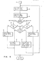
system clock 33 to the non-continuously clocked devices in the system is shown in the flow chart of Fig. 6. Step 101 indicates that a stop clock command is issued to the stop clock circuitry within stop clock control 32. Note that if the stop clock circuitry has not been previously armed, or has been disarmed by an event already occurring, then no stopping of the clocking signal fromoutput 40 will occur. After thesleep clock 51 has been restarted, i.e., sleep clock 32 has once again begun outputting the clocking signal overoutput 40 to the clocked devices in the system by either a DMA request or by an interrupt request, thendecision block 102 is reached. As can be seen, if a time-out has not been requested, then system operation returns todecision block 67 in Fig. 4 or 69 in Fig. 5. However, if a time-out has been requested, then a time-out counter is checked indecision block 103 as to whether or not it is equal to 0. If the time-out counter is not equal to 0, then once again system operation returns todecision block step 104, then system operation returns once again to eitherdecision block - The flow charts of Fig. 7 and Fig. 8 explain the operation of the system while a program running on
CPU 11 is waiting for a keystroke to occur or for one of diskette drives 26 or 27 to be accessed, respectively. The flow chart of Fig. 7 details the operation of the system of the present invention as the program running onCPU 11 awaits a keystroke fromkeyboard 28. Instep 111, the running program invokes a wait-for-keyboard-event function by specifying that the program wait for a compare not equal. That is, the keyboard buffer start is not equal to the keyboard buffer end, thereby signifying that keyboard data has been received. This result describes a keyboard event. Addition-ally, no time limit is set for this keyboard event to occur. Instep 112, the sleep clock control circuitry is armed but the system clock continues to be provided overoutput 40. Instep 114, the start and end pointers of a keyboard buffer (not shown) are compared. If the start and end pointers are not equal, then this is an indication that the awaited for keyboard data has been received and there is no longer a need to wait for a further keyboard event. Subsequently, the keystroke which has been entered is processed. However, if the pointers are equal, then as shown in step 115, the system clock output overline 51 is halted by sleep clock control 32. Additionally, as shown instep 116, the execution byCPU 11 is stopped until either a direct memory access request or an interrupt request is presented to sleep clock control 32, which in turn resumes the outputting of the system clock overoutput 40 tobus 51. In step 117, CPU execution is resumed after the receipt of an interrupt, and instep 118, the scan code of the keystroke which was just received will be put into the keyboard buffer and the end pointer of the buffer will be incremented thereby making the start and end pointer of the buffer not equal. After the keystroke has been processed, step 119 indicates that execution is returned to the sleep routine, thereby rearming the sleep clock and determining that the keyboard event has occurred. - Similarly, the operation of an application program running on
CPU 11 is detailed in the flow chart of Fig. 8 while the program is accessing either of diskette drives 26 or 27. Instep 121, the executing program sends commands todiskette controller 19. When the last command has been sent todiskette controller 19, it begins performing the required operation on one ofdiskettes CPU 11.Diskette controller 19 will notifyCPU 11 of the completion of the operation or if an error occurs using an interrupt request through interrupt controller 12. In step 122, the executing program invokes a "wait for external event" routine and specifies a return operation when a diskette interrupt received flag has been set. When usingdiskette controller 19, a time-out period is set to cause the wait to be aborted if the event being waited for has not occurred within that time-out period. Instep 123, the stop clock control circuitry is armed, but the system clock continues to be provided overoutput 40 to the non-continuously clocked devices. Indecision block 124, a determination is made as to whether or not a diskette interrupt bit has been set. If the bit has been set, then this is an indication that a diskette interrupt has been received by interrupt controller 12 and so the "wait on external event" routine is exited in order to check to see if the diskette operation has been completed. - However, if the diskette interrupt bit has not been set, then a signal is sent to sleep clock control 32 to stop outputting a clocking signal over
output 40. The stopping of the clocking signal continues until either the next direct memory access request or until an interrupt request is received byCPU 11. Attendant with the stopping of the clocking, the execution ofCPU 11 is stopped until either the DMA request or an interrupt request is received. When either of the above two events occurs, then the execution ofCPU 11 is resumed as shown instep 128. In step 129, a determination is made as to whether or not either of diskette drives 26 or 27 were the device requesting the interrupt. If so, then an interrupt handler for one of diskette drives 26 or 27 will set the diskette interrupt received bit. Finally, in step 130 after the interrupt has been handled and processed, control is returned to the wait for external event routine to determine that the event has occurred. The wait routine is then exited.
Claims (9)
means for stopping the clock signal to the processor;
means for detecting an interrupt generated by an I/O device or a request for memory access; and,
means for restarting a clock signal to the processor in response to the detection of said interrupt.
means for arming the stopping means;
means for detecting an interrupt subsequent to arming the stopping means and prior to stopping the clock signal; and,
means for halting operation of said stopping means in response to the detection of the subsequent interrupt.
stopping the clock signal to the processor upon completion of a processor operation;
detecting an interrupt generated by an I/O device or a request for memory access subsequent to stopping said clock signal; and,
restarting the clock signal to the processor in response to the detection of said interrupt.
Applications Claiming Priority (2)
| Application Number | Priority Date | Filing Date | Title |
|---|---|---|---|
| US06/820,460 US4851987A (en) | 1986-01-17 | 1986-01-17 | System for reducing processor power consumption by stopping processor clock supply if a desired event does not occur |
| US820460 | 1986-01-17 |
Publications (3)
| Publication Number | Publication Date |
|---|---|
| EP0229692A2 true EP0229692A2 (en) | 1987-07-22 |
| EP0229692A3 EP0229692A3 (en) | 1988-01-13 |
| EP0229692B1 EP0229692B1 (en) | 1992-04-29 |
Family
ID=25230819
Family Applications (1)
| Application Number | Title | Priority Date | Filing Date |
|---|---|---|---|
| EP87300118A Expired - Fee Related EP0229692B1 (en) | 1986-01-17 | 1987-01-08 | Data processing apparatus |
Country Status (9)
| Country | Link |
|---|---|
| US (1) | US4851987A (en) |
| EP (1) | EP0229692B1 (en) |
| JP (1) | JPS62169219A (en) |
| CN (1) | CN1003961B (en) |
| AR (1) | AR242669A1 (en) |
| BR (1) | BR8606400A (en) |
| DE (1) | DE3778558D1 (en) |
| HK (1) | HK88292A (en) |
| SG (1) | SG93592G (en) |
Cited By (10)
| Publication number | Priority date | Publication date | Assignee | Title |
|---|---|---|---|---|
| EP0343528A2 (en) * | 1988-05-21 | 1989-11-29 | Fujitsu Limited | Mobile telephone terminal |
| EP0458756A1 (en) * | 1990-04-26 | 1991-11-27 | STMicroelectronics S.r.l. | Data transfer in DMA mode during a wake up phase of a microprocessor in a wait for interrupt condition for reducing power consumption |
| GB2246455A (en) * | 1990-07-23 | 1992-01-29 | Philips Electronic Associated | Altering the rate at which digital circuitry operates |
| EP0479887A1 (en) * | 1989-06-30 | 1992-04-15 | Fujitsu Personal Systems, Inc. | Computer power management system |
| EP0579369A1 (en) * | 1992-07-14 | 1994-01-19 | Advanced Micro Devices, Inc. | Central processing unit with reduced power consumption |
| EP0582391A1 (en) * | 1992-07-21 | 1994-02-09 | Advanced Micro Devices, Inc. | Clock generator with power savings capability |
| EP0624837A1 (en) * | 1993-05-13 | 1994-11-17 | International Business Machines Corporation | Electronic apparatus with reduced power consumption |
| EP1237066A2 (en) * | 1992-03-27 | 2002-09-04 | National Semiconductor Corporation | Microprocessor with hardware controlled power management and selectable input/output control pins |
| KR100358889B1 (en) * | 1994-10-19 | 2003-01-24 | 아드밴스트 마이크로 디이바이시스 인코포레이티드 | Integrated processor system suitable for portable personal information equipment |
| EP2336846A1 (en) * | 2009-11-20 | 2011-06-22 | Nxp B.V. | Event-driven processor architecture |
Families Citing this family (165)
| Publication number | Priority date | Publication date | Assignee | Title |
|---|---|---|---|---|
| JPH0542505Y2 (en) * | 1988-03-14 | 1993-10-26 | ||
| DK174975B1 (en) * | 1988-05-06 | 2004-04-05 | Toppan Printing Co Ltd | Integrated circuit board |
| JPH0776984B2 (en) * | 1988-05-06 | 1995-08-16 | 凸版印刷株式会社 | IC card |
| US5050113A (en) * | 1988-06-17 | 1991-09-17 | Dallas Semiconductor Corporation | Low power timekeeping system |
| US5003501A (en) * | 1988-06-07 | 1991-03-26 | Dallas Semiconductor Corporation | Precharge circuitry and bus for low power applications |
| US5629907A (en) * | 1991-06-18 | 1997-05-13 | Dallas Semiconductor Corporation | Low power timekeeping system |
| US5347472A (en) * | 1988-06-17 | 1994-09-13 | Dallas Semiconductor Corporation | Precharge circuitry and bus for low power applications |
| US5544078A (en) * | 1988-06-17 | 1996-08-06 | Dallas Semiconductor Corporation | Timekeeping comparison circuitry and dual storage memory cells to detect alarms |
| JPH0719211B2 (en) * | 1988-10-08 | 1995-03-06 | 日本電気株式会社 | Clock control system |
| US4980836A (en) * | 1988-10-14 | 1990-12-25 | Compaq Computer Corporation | Apparatus for reducing computer system power consumption |
| US5182810A (en) * | 1989-05-31 | 1993-01-26 | Dallas Semiconductor Corp. | Isolation gates to permit selective power-downs within a closely-coupled multi-chip system |
| US5203000A (en) * | 1988-12-09 | 1993-04-13 | Dallas Semiconductor Corp. | Power-up reset conditioned on direction of voltage change |
| US5590343A (en) * | 1988-12-09 | 1996-12-31 | Dallas Semiconductor Corporation | Touch-sensitive switching circuitry for power-up |
| US5175845A (en) * | 1988-12-09 | 1992-12-29 | Dallas Semiconductor Corp. | Integrated circuit with watchdog timer and sleep control logic which places IC and watchdog timer into sleep mode |
| US5754462A (en) * | 1988-12-09 | 1998-05-19 | Dallas Semiconductor Corporation | Microprocessor auxiliary with ability to be queried re power history |
| WO1990006555A1 (en) * | 1988-12-09 | 1990-06-14 | Dallas Semiconductor Corporation | Auxiliary integrated circuit for microprocessor management |
| WO1990006553A1 (en) * | 1988-12-09 | 1990-06-14 | Dallas Semiconductor Corporation | Low-power system with microprocessor and ancillary chip |
| US5123102A (en) * | 1988-12-19 | 1992-06-16 | Hewlett-Packard Company | Method and apparatus for suspending computation due to detection of electrostatic discharge |
| US5123107A (en) * | 1989-06-20 | 1992-06-16 | Mensch Jr William D | Topography of CMOS microcomputer integrated circuit chip including core processor and memory, priority, and I/O interface circuitry coupled thereto |
| US5142684A (en) * | 1989-06-23 | 1992-08-25 | Hand Held Products, Inc. | Power conservation in microprocessor controlled devices |
| US5222239A (en) * | 1989-07-28 | 1993-06-22 | Prof. Michael H. Davis | Process and apparatus for reducing power usage microprocessor devices operating from stored energy sources |
| US5167024A (en) * | 1989-09-08 | 1992-11-24 | Apple Computer, Inc. | Power management for a laptop computer with slow and sleep modes |
| JP2750172B2 (en) * | 1989-10-06 | 1998-05-13 | キヤノン株式会社 | Electronics |
| US5218704A (en) * | 1989-10-30 | 1993-06-08 | Texas Instruments | Real-time power conservation for portable computers |
| US6158012A (en) * | 1989-10-30 | 2000-12-05 | Texas Instruments Incorporated | Real-time power conservation and thermal management for computers |
| US5247655A (en) * | 1989-11-07 | 1993-09-21 | Chips And Technologies, Inc. | Sleep mode refresh apparatus |
| US5201059A (en) * | 1989-11-13 | 1993-04-06 | Chips And Technologies, Inc. | Method for reducing power consumption includes comparing variance in number of time microprocessor tried to react input in predefined period to predefined variance |
| ES2045864T3 (en) * | 1989-12-19 | 1994-01-16 | Jaeger | CONTROL PROCEDURE OF A RAD OF ELECTRONIC STATIONS AND NETWORK OBTAINED, IN PARTICULAR FOR AUTOMOBILE VEHICLE. |
| JPH03212717A (en) * | 1990-01-18 | 1991-09-18 | Fujitsu Ltd | Power supply control system |
| US5081586A (en) * | 1990-02-20 | 1992-01-14 | Eaton Corporation | Multiplexing of accessories in a vehicle |
| JPH03248236A (en) * | 1990-02-26 | 1991-11-06 | Mitsubishi Electric Corp | Wait controller |
| US6795929B2 (en) * | 1990-03-23 | 2004-09-21 | Matsushita Electric Industrial Co., Ltd. | Data processing apparatus |
| EP0448350B1 (en) | 1990-03-23 | 1996-12-27 | Matsushita Electric Industrial Co., Ltd. | Hand held data processing apparatus having reduced power consumption |
| US5355503A (en) * | 1990-05-31 | 1994-10-11 | National Semiconductor Corporation | Event driven scanning of data input equipment using multi-input wake-up techniques |
| US5303390A (en) * | 1990-06-28 | 1994-04-12 | Dallas Semiconductor Corporation | Microprocessor auxiliary with combined pin for reset output and pushbutton input |
| JPH04130510A (en) * | 1990-09-21 | 1992-05-01 | Hitachi Ltd | Power saving system for information processor |
| WO1992007317A1 (en) * | 1990-10-12 | 1992-04-30 | Intel Corporation | Slow memory refresh in a computer with a limited supply of power |
| US5237692A (en) * | 1990-11-09 | 1993-08-17 | Ast Research Inc. | Internal interrupt controller for a peripheral controller |
| US5280283A (en) * | 1990-11-09 | 1994-01-18 | Ast Research, Inc. | Memory mapped keyboard controller |
| US5560017A (en) * | 1990-11-09 | 1996-09-24 | Wang Laboratories, Inc. | System with clock frequency controller responsive to interrupt independent of software routine and software loop repeatedly executing instruction to slow down system clock |
| JPH0511876A (en) * | 1990-12-25 | 1993-01-22 | Mitsubishi Electric Corp | Digital circuit device |
| US5414860A (en) * | 1991-01-29 | 1995-05-09 | International Business Machines Incorporated | Power management initialization for a computer operable under a plurality of operating systems |
| US5239652A (en) * | 1991-02-04 | 1993-08-24 | Apple Computer, Inc. | Arrangement for reducing computer power consumption by turning off the microprocessor when inactive |
| FI88657C (en) * | 1991-02-12 | 1993-06-10 | Nokia Mobile Phones Ltd | Foerfarande Foer att minska stroemfoerbrukningen i en mobil telefon |
| US5410711A (en) * | 1991-02-14 | 1995-04-25 | Dell Usa, L.P. | Portable computer with BIOS-independent power management |
| US5566340A (en) * | 1991-02-14 | 1996-10-15 | Dell Usa L.P. | Portable computer system with adaptive power control parameters |
| JPH0776894B2 (en) * | 1991-02-25 | 1995-08-16 | インターナショナル・ビジネス・マシーンズ・コーポレイション | Clock signal control method for processor and information processing system |
| EP0503659A1 (en) * | 1991-03-15 | 1992-09-16 | Nippon Steel Corporation | System interruption apparatus |
| US5203003A (en) * | 1991-03-28 | 1993-04-13 | Echelon Corporation | Computer architecture for conserving power by using shared resources and method for suspending processor execution in pipeline |
| JPH04333119A (en) * | 1991-05-09 | 1992-11-20 | Matsushita Electric Ind Co Ltd | Information processor |
| US5319785A (en) * | 1991-06-28 | 1994-06-07 | Digital Equipment Corporation | Polling of I/O device status comparison performed in the polled I/O device |
| US5355484A (en) * | 1991-08-12 | 1994-10-11 | International Business Machines Corporation | Dynamically established event monitors in event management services of a computer system |
| US5625821A (en) * | 1991-08-12 | 1997-04-29 | International Business Machines Corporation | Asynchronous or synchronous operation of event signaller by event management services in a computer system |
| US5305454A (en) * | 1991-08-12 | 1994-04-19 | International Business Machines Corporation | Notification of event handlers in broadcast or propagation mode by event management services in a computer system |
| US5237684A (en) * | 1991-08-12 | 1993-08-17 | International Business Machines Corporation | Customized and versatile event monitor within event management services of a computer system |
| JPH05108218A (en) * | 1991-10-11 | 1993-04-30 | Toshiba Corp | Computer system |
| US5832286A (en) * | 1991-12-04 | 1998-11-03 | Sharp Kabushiki Kaisha | Power control apparatus for digital electronic device |
| JP3237926B2 (en) * | 1991-12-04 | 2001-12-10 | シャープ株式会社 | Power control device for digital electronic device, processing device provided with the power control device, and power management system for digital electronic device provided with the processing device |
| US5369771A (en) * | 1991-12-23 | 1994-11-29 | Dell U.S.A., L.P. | Computer with transparent power-saving manipulation of CPU clock |
| US6343363B1 (en) | 1994-09-22 | 2002-01-29 | National Semiconductor Corporation | Method of invoking a low power mode in a computer system using a halt instruction |
| US5630143A (en) * | 1992-03-27 | 1997-05-13 | Cyrix Corporation | Microprocessor with externally controllable power management |
| US5423045A (en) * | 1992-04-15 | 1995-06-06 | International Business Machines Corporation | System for distributed power management in portable computers |
| US5404543A (en) * | 1992-05-29 | 1995-04-04 | International Business Machines Corporation | Method and system for reducing an amount of power utilized by selecting a lowest power mode from a plurality of power modes |
| DE69320417T3 (en) * | 1992-06-12 | 2004-05-19 | Texas Instruments Inc., Dallas | Process and device for changing the clock frequency of a processor |
| US5485625A (en) * | 1992-06-29 | 1996-01-16 | Ford Motor Company | Method and apparatus for monitoring external events during a microprocessor's sleep mode |
| US5324992A (en) * | 1992-07-01 | 1994-06-28 | Carnegie Mellon University | Self-timing integrated circuits having low clock signal during inactive periods |
| US5404459A (en) * | 1992-07-21 | 1995-04-04 | Advanced Micro Devices | Serial interface module and method in which the clock is only activated to send a predetermined number of data bits |
| US5287292A (en) * | 1992-10-16 | 1994-02-15 | Picopower Technology, Inc. | Heat regulator for integrated circuits |
| US5392437A (en) * | 1992-11-06 | 1995-02-21 | Intel Corporation | Method and apparatus for independently stopping and restarting functional units |
| US5339445A (en) * | 1992-11-16 | 1994-08-16 | Harris Corporation | Method of autonomously reducing power consumption in a computer sytem by compiling a history of power consumption |
| US5457781A (en) * | 1993-01-04 | 1995-10-10 | Amdahl Corporation | System having main unit for shutting off clocks to memory upon completion of writing data into memory and information supervising unit to read the data |
| US5630144A (en) * | 1993-02-19 | 1997-05-13 | Phoenix Technologies Ltd. | Desktop computer monitor power control using keyboard controller |
| US5603036A (en) * | 1993-02-19 | 1997-02-11 | Intel Corporation | Power management system for components used in battery powered applications |
| US5485623A (en) * | 1993-03-10 | 1996-01-16 | Hitachi, Ltd. | Information processor having high speed and safety resume system |
| US5692203A (en) * | 1993-03-12 | 1997-11-25 | Psc, Inc. | Power up/power down for electronic hardware which conserves electric power |
| US5579206A (en) * | 1993-07-16 | 1996-11-26 | Dallas Semiconductor Corporation | Enhanced low profile sockets and module systems |
| US5528463A (en) * | 1993-07-16 | 1996-06-18 | Dallas Semiconductor Corp. | Low profile sockets and modules for surface mountable applications |
| US5497494A (en) * | 1993-07-23 | 1996-03-05 | International Business Machines Corporation | Method for saving and restoring the state of a CPU executing code in protected mode |
| US5513359A (en) * | 1993-07-23 | 1996-04-30 | International Business Machines Corporation | Desktop computer having a single-switch suspend/resume function |
| AU732436B2 (en) * | 1993-07-26 | 2001-04-26 | Lenovo (Singapore) Pte. Ltd. | Desktop computer system having multi-level power management |
| US5913071A (en) * | 1993-07-26 | 1999-06-15 | National Semiconductor Corporation | Scalar interrupt-acknowledgement system that responds to a plurality of events with a single interrupt signal |
| US5548763A (en) * | 1993-07-26 | 1996-08-20 | International Business Machines Corporation | Desk top computer system having multi-level power management |
| US5511202A (en) * | 1993-07-26 | 1996-04-23 | International Business Machines Corporation | Desktop computer system having zero-volt system suspend and control unit for ascertaining interrupt controller base address |
| US5408668A (en) * | 1993-07-28 | 1995-04-18 | Tornai; Richard | Method and apparatus for controlling the provision of power to computer peripherals |
| US7216064B1 (en) * | 1993-09-21 | 2007-05-08 | Intel Corporation | Method and apparatus for programmable thermal sensor for an integrated circuit |
| US5894577A (en) * | 1993-09-22 | 1999-04-13 | Advanced Micro Devices, Inc. | Interrupt controller with external in-service indication for power management within a computer system |
| DE69432697T2 (en) * | 1993-12-01 | 2004-03-25 | Advanced Micro Devices, Inc., Sunnyvale | Power management for computer system and method therefor |
| JPH07182857A (en) * | 1993-12-24 | 1995-07-21 | Toshiba Corp | Microcomputer system |
| US5706407A (en) * | 1993-12-28 | 1998-01-06 | Kabushiki Kaisha Toshiba | System for reallocation of memory banks in memory sized order |
| US5546568A (en) * | 1993-12-29 | 1996-08-13 | Intel Corporation | CPU clock control unit |
| CA2113492A1 (en) * | 1994-01-14 | 1995-07-15 | Donald W. Church | Apparatus and method for identifying metallic tokens and coins |
| US5640573A (en) * | 1994-02-02 | 1997-06-17 | Advanced Micro Devices, Inc. | Power management message bus for integrated processor |
| EP0666529B1 (en) * | 1994-02-02 | 2004-10-06 | Advanced Micro Devices, Inc. | Power management in an asynchronus receiver/transmitter |
| US5493684A (en) * | 1994-04-06 | 1996-02-20 | Advanced Micro Devices | Power management architecture including a power management messaging bus for conveying an encoded activity signal for optimal flexibility |
| WO1995028671A1 (en) * | 1994-04-18 | 1995-10-26 | Green Logic Inc. | An improved system logic controller for digital computers |
| US7167993B1 (en) | 1994-06-20 | 2007-01-23 | Thomas C Douglass | Thermal and power management for computer systems |
| US5752011A (en) | 1994-06-20 | 1998-05-12 | Thomas; C. Douglas | Method and system for controlling a processor's clock frequency in accordance with the processor's temperature |
| KR960012838B1 (en) * | 1994-06-20 | 1996-09-24 | 삼성전자 주식회사 | Controller for stop-clock and method therefor |
| US5721934A (en) * | 1994-06-29 | 1998-02-24 | Intel Corporation | Retrofit external power saving system and method for use |
| US5511204A (en) * | 1994-09-07 | 1996-04-23 | International Business Machines Corporation | Performing system tasks at power-off using system management interrupt |
| US5530879A (en) * | 1994-09-07 | 1996-06-25 | International Business Machines Corporation | Computer system having power management processor for switching power supply from one state to another responsive to a closure of a switch, a detected ring or an expiration of a timer |
| US5590341A (en) * | 1994-09-30 | 1996-12-31 | Intel Corporation | Method and apparatus for reducing power consumption in a computer system using ready delay |
| US5754869A (en) * | 1994-10-04 | 1998-05-19 | Intel Corporation | Method and apparatus for managing power consumption of the CPU and on-board system devices of personal computers |
| JPH08147064A (en) * | 1994-11-24 | 1996-06-07 | Mitsubishi Denki Semiconductor Software Kk | Intermittent operating circuit |
| JP2885112B2 (en) * | 1995-01-27 | 1999-04-19 | 株式会社デンソー | Semiconductor integrated circuit |
| JPH08202468A (en) * | 1995-01-27 | 1996-08-09 | Hitachi Ltd | Multiprocessor system |
| US5724592A (en) * | 1995-03-31 | 1998-03-03 | Intel Corporation | Method and apparatus for managing active power consumption in a microprocessor controlled storage device |
| CA2173428A1 (en) | 1995-04-06 | 1996-10-07 | Donald W. Church | Electronic parking meter |
| GB2301202B (en) * | 1995-05-19 | 1999-09-22 | Advanced Risc Mach Ltd | Controlling processing clock signals |
| TW327707B (en) * | 1995-05-18 | 1998-03-01 | Motorola Inc | Method for producing power consumption in a portable electronic device with a liquid crystal display screen |
| JPH08328684A (en) | 1995-05-30 | 1996-12-13 | Toshiba Corp | Computer system |
| JP3075957B2 (en) | 1995-05-30 | 2000-08-14 | 株式会社東芝 | Computer system |
| US5752044A (en) * | 1995-06-07 | 1998-05-12 | International Business Machines Corporation | Computer system having multi-level suspend timers to suspend from operation in attended and unattended modes |
| US5587672A (en) * | 1995-09-25 | 1996-12-24 | Neomagic Corp. | Dynamic logic having power-down mode with periodic clock refresh for a low-power graphics controller |
| US5708819A (en) * | 1995-10-10 | 1998-01-13 | Standard Microsystems Corporation | Process and apparatus for generating power management events in a computer system |
| JP3621497B2 (en) * | 1996-03-01 | 2005-02-16 | 株式会社東芝 | Computer system and clock stop signal control method in the same system |
| DE19608776C2 (en) * | 1996-03-07 | 2003-03-20 | Atmel Germany Gmbh | Integrated circuit arrangement with a bus logic unit connected to a data bus |
| US5983355A (en) * | 1996-05-20 | 1999-11-09 | National Semiconductor Corporation | Power conservation method and apparatus activated by detecting specific fixed interrupt signals indicative of system inactivity and excluding prefetched signals |
| US5848281A (en) * | 1996-07-23 | 1998-12-08 | Smalley; Kenneth George | Method and apparatus for powder management in a multifunction controller with an embedded microprocessor |
| US5790609A (en) * | 1996-11-04 | 1998-08-04 | Texas Instruments Incorporated | Apparatus for cleanly switching between various clock sources in a data processing system |
| US5903746A (en) * | 1996-11-04 | 1999-05-11 | Texas Instruments Incorporated | Apparatus and method for automatically sequencing clocks in a data processing system when entering or leaving a low power state |
| US5949261A (en) | 1996-12-17 | 1999-09-07 | Cypress Semiconductor Corp. | Method and circuit for reducing power and/or current consumption |
| US6055489A (en) * | 1997-04-15 | 2000-04-25 | Intel Corporation | Temperature measurement and compensation scheme |
| US5964881A (en) * | 1997-11-11 | 1999-10-12 | Advanced Micro Devices | System and method to control microprocessor startup to reduce power supply bulk capacitance needs |
| US6895448B2 (en) | 1998-03-26 | 2005-05-17 | O2 Micro, Inc. | Low-power audio CD player for portable computers |
| US6675233B1 (en) * | 1998-03-26 | 2004-01-06 | O2 Micro International Limited | Audio controller for portable electronic devices |
| US6954804B2 (en) * | 1998-03-26 | 2005-10-11 | Micro, Inc. | Controller for portable electronic devices |
| US6125440A (en) * | 1998-05-21 | 2000-09-26 | Tellabs Operations, Inc. | Storing executing instruction sequence for re-execution upon backward branch to reduce power consuming memory fetch |
| DE19830068A1 (en) * | 1998-06-30 | 2000-01-05 | Teles Ag | Method for controlling certain modes or functions of a terminal connected to a bus |
| US6393374B1 (en) | 1999-03-30 | 2002-05-21 | Intel Corporation | Programmable thermal management of an integrated circuit die |
| US6363490B1 (en) | 1999-03-30 | 2002-03-26 | Intel Corporation | Method and apparatus for monitoring the temperature of a processor |
| US6606674B1 (en) * | 2000-02-24 | 2003-08-12 | Intel Corporation | Method and apparatus for reducing circular list's thrashing by detecting the queues' status on a circular linked list |
| US6665802B1 (en) | 2000-02-29 | 2003-12-16 | Infineon Technologies North America Corp. | Power management and control for a microcontroller |
| US7263567B1 (en) | 2000-09-25 | 2007-08-28 | Intel Corporation | Method and apparatus for lowering the die temperature of a microprocessor and maintaining the temperature below the die burn out |
| US7522966B2 (en) * | 2000-12-01 | 2009-04-21 | O2Micro International Limited | Low power digital audio decoding/playing system for computing devices |
| US7522965B2 (en) | 2000-12-01 | 2009-04-21 | O2Micro International Limited | Low power digital audio decoding/playing system for computing devices |
| US7526349B2 (en) * | 2000-12-01 | 2009-04-28 | O2Micro International Limited | Low power digital audio decoding/playing system for computing devices |
| US7818443B2 (en) * | 2000-12-01 | 2010-10-19 | O2Micro International Ltd. | Low power digital audio decoding/playing system for computing devices |
| US7890741B2 (en) * | 2000-12-01 | 2011-02-15 | O2Micro International Limited | Low power digital audio decoding/playing system for computing devices |
| US7522964B2 (en) | 2000-12-01 | 2009-04-21 | O2Micro International Limited | Low power digital audio decoding/playing system for computing devices |
| US7069367B2 (en) * | 2000-12-29 | 2006-06-27 | Intel Corporation | Method and apparatus for avoiding race condition with edge-triggered interrupts |
| US6768362B1 (en) | 2001-08-13 | 2004-07-27 | Cypress Semiconductor Corp. | Fail-safe zero delay buffer with automatic internal reference |
| JP2003058272A (en) * | 2001-08-21 | 2003-02-28 | Mitsubishi Electric Corp | Semiconductor device and semiconductor chip used in the same |
| US7337333B2 (en) * | 2001-09-19 | 2008-02-26 | Dell Products L.P. | System and method for strategic power supply sequencing in a computer system with multiple processing resources and multiple power supplies |
| US7325050B2 (en) * | 2001-09-19 | 2008-01-29 | Dell Products L.P. | System and method for strategic power reduction in a computer system |
| US7111179B1 (en) | 2001-10-11 | 2006-09-19 | In-Hand Electronics, Inc. | Method and apparatus for optimizing performance and battery life of electronic devices based on system and application parameters |
| JP4079653B2 (en) * | 2002-02-22 | 2008-04-23 | 三洋電機株式会社 | Clock control method and clock control circuit |
| US7670224B2 (en) * | 2002-04-03 | 2010-03-02 | Igt | Gaming apparatus with power saving feature |
| US6924667B2 (en) | 2002-07-19 | 2005-08-02 | O2Micro International Limited | Level shifting and level-shifting amplifier circuits |
| JP2004078581A (en) * | 2002-08-19 | 2004-03-11 | Nec Corp | Communication data processing circuit |
| CN1327344C (en) * | 2003-08-19 | 2007-07-18 | 英特尔公司 | Bios for saving and restoring operational state in the absence of AC power |
| US8250406B2 (en) * | 2003-08-19 | 2012-08-21 | Intel Corporation | Operational state preservation in the absence of AC power |
| US20060026530A1 (en) * | 2004-07-30 | 2006-02-02 | Texas Instruments Incorporated | DMA overlay addressing methodology for optimizing power and improving memory bandwidth for display engines |
| JP3870970B2 (en) * | 2005-03-15 | 2007-01-24 | セイコーエプソン株式会社 | Processor control unit |
| US8627116B2 (en) * | 2007-08-07 | 2014-01-07 | Maxim Integrated Products, Inc. | Power conservation in an intrusion detection system |
| US8184019B2 (en) | 2008-04-25 | 2012-05-22 | J.J. Mackay Canada Limited | Data collection system for electronic parking meters |
| JP4711269B2 (en) * | 2008-11-21 | 2011-06-29 | インターナショナル・ビジネス・マシーンズ・コーポレーション | Memory power control method and memory power control program |
| US20100146169A1 (en) * | 2008-12-05 | 2010-06-10 | Nuvoton Technology Corporation | Bus-handling |
| WO2010071972A1 (en) | 2008-12-23 | 2010-07-01 | J.J.Mackay Canada Limited | Low power wireless parking meter and parking meter network |
| US7907003B2 (en) * | 2009-01-14 | 2011-03-15 | Standard Microsystems Corporation | Method for improving power-supply rejection |
| CA3178279A1 (en) | 2011-03-03 | 2012-09-03 | J.J. Mackay Canada Limited | Parking meter with contactless payment |
| CA145137S (en) | 2012-04-02 | 2013-07-22 | Jj Mackay Canada Ltd | Single space parking meter |
| CA2894350C (en) | 2015-06-16 | 2023-03-28 | J.J. Mackay Canada Limited | Coin chute with anti-fishing assembly |
| US11922756B2 (en) | 2019-01-30 | 2024-03-05 | J.J. Mackay Canada Limited | Parking meter having touchscreen display |
| CA3031936A1 (en) | 2019-01-30 | 2020-07-30 | J.J. Mackay Canada Limited | Spi keyboard module for a parking meter and a parking meter having an spi keyboard module |
Citations (3)
| Publication number | Priority date | Publication date | Assignee | Title |
|---|---|---|---|---|
| US4077011A (en) * | 1976-12-20 | 1978-02-28 | International Business Machines Corporation | Uncertain interval timer using a variable length shift register |
| US4218876A (en) * | 1976-11-29 | 1980-08-26 | Sharp Kabushiki Kaisha | Combined timekeeper and calculator with low power consumption features |
| US4293927A (en) * | 1979-12-12 | 1981-10-06 | Casio Computer Co., Ltd. | Power consumption control system for electronic digital data processing devices |
Family Cites Families (23)
| Publication number | Priority date | Publication date | Assignee | Title |
|---|---|---|---|---|
| US3411147A (en) * | 1966-03-24 | 1968-11-12 | Burroughs Corp | Apparatus for executing halt instructions in a multi-program processor |
| US3941989A (en) * | 1974-12-13 | 1976-03-02 | Mos Technology, Inc. | Reducing power consumption in calculators |
| US4203153A (en) * | 1978-04-12 | 1980-05-13 | Diebold, Incorporated | Circuit for reducing power consumption in battery operated microprocessor based systems |
| US4279020A (en) * | 1978-08-18 | 1981-07-14 | Bell Telephone Laboratories, Incorporated | Power supply circuit for a data processor |
| DE2911998C2 (en) * | 1979-03-27 | 1985-11-07 | Robert Bosch Gmbh, 7000 Stuttgart | Power supply for a microprocessor that controls electrical devices, in particular a motor vehicle |
| US4758945A (en) * | 1979-08-09 | 1988-07-19 | Motorola, Inc. | Method for reducing power consumed by a static microprocessor |
| JPS5950072B2 (en) * | 1979-09-13 | 1984-12-06 | カシオ計算機株式会社 | Auto power off device |
| JPS5654529A (en) * | 1979-10-08 | 1981-05-14 | Nec Corp | Data processor |
| US4316247A (en) * | 1979-10-30 | 1982-02-16 | Texas Instruments, Inc. | Low power consumption data processing system |
| US4409665A (en) * | 1979-12-26 | 1983-10-11 | Texas Instruments Incorporated | Turn-off-processor between keystrokes |
| US4317180A (en) * | 1979-12-26 | 1982-02-23 | Texas Instruments Incorporated | Clocked logic low power standby mode |
| GB2080585B (en) * | 1980-07-22 | 1984-07-04 | Tokyo Shibaura Electric Co | Semiconductor integrated circuit with reduced power consumption |
| JPS5775335A (en) * | 1980-10-27 | 1982-05-11 | Hitachi Ltd | Data processor |
| JPS58222349A (en) * | 1982-06-18 | 1983-12-24 | Nec Corp | Information processor |
| US4545030A (en) * | 1982-09-28 | 1985-10-01 | The John Hopkins University | Synchronous clock stopper for microprocessor |
| US4698748A (en) * | 1983-10-07 | 1987-10-06 | Essex Group, Inc. | Power-conserving control system for turning-off the power and the clocking for data transactions upon certain system inactivity |
| US4780843A (en) * | 1983-11-07 | 1988-10-25 | Motorola, Inc. | Wait mode power reduction system and method for data processor |
| US4573117A (en) * | 1983-11-07 | 1986-02-25 | Motorola, Inc. | Method and apparatus in a data processor for selectively disabling a power-down instruction |
| US4586179A (en) * | 1983-12-09 | 1986-04-29 | Zenith Electronics Corporation | Microprocessor reset with power level detection and watchdog timer |
| JPS60154709A (en) * | 1984-01-25 | 1985-08-14 | Toshiba Corp | Clock signal generating circuit |
| US4627085A (en) * | 1984-06-29 | 1986-12-02 | Applied Micro Circuits Corporation | Flip-flop control circuit |
| US4665328A (en) * | 1984-07-27 | 1987-05-12 | National Semiconductor Corporation | Multiple clock power down method and structure |
| US4757505A (en) * | 1986-04-30 | 1988-07-12 | Elgar Electronics Corp. | Computer power system |
-
1986
- 1986-01-17 US US06/820,460 patent/US4851987A/en not_active Expired - Lifetime
- 1986-12-08 CN CN86108202.8A patent/CN1003961B/en not_active Expired
- 1986-12-16 JP JP61297873A patent/JPS62169219A/en active Pending
- 1986-12-23 BR BR8606400A patent/BR8606400A/en not_active IP Right Cessation
-
1987
- 1987-01-06 AR AR87306507A patent/AR242669A1/en active
- 1987-01-08 DE DE8787300118T patent/DE3778558D1/en not_active Expired - Fee Related
- 1987-01-08 EP EP87300118A patent/EP0229692B1/en not_active Expired - Fee Related
-
1992
- 1992-09-15 SG SG935/92A patent/SG93592G/en unknown
- 1992-11-12 HK HK882/92A patent/HK88292A/en not_active IP Right Cessation
Patent Citations (3)
| Publication number | Priority date | Publication date | Assignee | Title |
|---|---|---|---|---|
| US4218876A (en) * | 1976-11-29 | 1980-08-26 | Sharp Kabushiki Kaisha | Combined timekeeper and calculator with low power consumption features |
| US4077011A (en) * | 1976-12-20 | 1978-02-28 | International Business Machines Corporation | Uncertain interval timer using a variable length shift register |
| US4293927A (en) * | 1979-12-12 | 1981-10-06 | Casio Computer Co., Ltd. | Power consumption control system for electronic digital data processing devices |
Cited By (22)
| Publication number | Priority date | Publication date | Assignee | Title |
|---|---|---|---|---|
| EP0343528A2 (en) * | 1988-05-21 | 1989-11-29 | Fujitsu Limited | Mobile telephone terminal |
| EP0757466A3 (en) * | 1988-05-21 | 1997-08-13 | Fujitsu Ltd | Mobile telephone terminal with power saving means |
| EP0757466A2 (en) * | 1988-05-21 | 1997-02-05 | Fujitsu Limited | Mobile telephone terminal with power saving means |
| EP0343528A3 (en) * | 1988-05-21 | 1992-03-04 | Fujitsu Limited | Mobile telephone terminal |
| EP0479887A4 (en) * | 1989-06-30 | 1992-08-12 | Poqet Computer Corporation | Computer power management system |
| US5428790A (en) * | 1989-06-30 | 1995-06-27 | Fujitsu Personal Systems, Inc. | Computer power management system |
| EP0479887A1 (en) * | 1989-06-30 | 1992-04-15 | Fujitsu Personal Systems, Inc. | Computer power management system |
| US5560024A (en) * | 1989-06-30 | 1996-09-24 | Fujitsu Personal Systems, Inc. | Computer power management system |
| EP0458756A1 (en) * | 1990-04-26 | 1991-11-27 | STMicroelectronics S.r.l. | Data transfer in DMA mode during a wake up phase of a microprocessor in a wait for interrupt condition for reducing power consumption |
| GB2246455A (en) * | 1990-07-23 | 1992-01-29 | Philips Electronic Associated | Altering the rate at which digital circuitry operates |
| EP1237066A2 (en) * | 1992-03-27 | 2002-09-04 | National Semiconductor Corporation | Microprocessor with hardware controlled power management and selectable input/output control pins |
| EP1237066A3 (en) * | 1992-03-27 | 2002-09-25 | National Semiconductor Corporation | Microprocessor with hardware controlled power management and selectable input/output control pins |
| US5452434A (en) * | 1992-07-14 | 1995-09-19 | Advanced Micro Devices, Inc. | Clock control for power savings in high performance central processing units |
| EP0579369A1 (en) * | 1992-07-14 | 1994-01-19 | Advanced Micro Devices, Inc. | Central processing unit with reduced power consumption |
| US5502689A (en) * | 1992-07-21 | 1996-03-26 | Advanced Micro Devices, Inc. | Clock generator capable of shut-down mode and clock generation method |
| EP0582391A1 (en) * | 1992-07-21 | 1994-02-09 | Advanced Micro Devices, Inc. | Clock generator with power savings capability |
| CN1052548C (en) * | 1992-07-21 | 2000-05-17 | 先进显微设备股份有限公司 | Clock generator capable of shut-down mode and clock generation method |
| US5420808A (en) * | 1993-05-13 | 1995-05-30 | International Business Machines Corporation | Circuitry and method for reducing power consumption within an electronic circuit |
| EP0624837A1 (en) * | 1993-05-13 | 1994-11-17 | International Business Machines Corporation | Electronic apparatus with reduced power consumption |
| KR100358889B1 (en) * | 1994-10-19 | 2003-01-24 | 아드밴스트 마이크로 디이바이시스 인코포레이티드 | Integrated processor system suitable for portable personal information equipment |
| EP2336846A1 (en) * | 2009-11-20 | 2011-06-22 | Nxp B.V. | Event-driven processor architecture |
| US10198062B2 (en) | 2009-11-20 | 2019-02-05 | Nxp B.V. | Microprocessor to resume clocking and execution based on external input pattern detection |
Also Published As
| Publication number | Publication date |
|---|---|
| AR242669A1 (en) | 1993-04-30 |
| CN1003961B (en) | 1989-04-19 |
| HK88292A (en) | 1992-11-20 |
| EP0229692A3 (en) | 1988-01-13 |
| SG93592G (en) | 1992-12-04 |
| DE3778558D1 (en) | 1992-06-04 |
| CN86108202A (en) | 1987-07-29 |
| US4851987A (en) | 1989-07-25 |
| JPS62169219A (en) | 1987-07-25 |
| BR8606400A (en) | 1987-10-13 |
| EP0229692B1 (en) | 1992-04-29 |
Similar Documents
| Publication | Publication Date | Title |
|---|---|---|
| US4851987A (en) | System for reducing processor power consumption by stopping processor clock supply if a desired event does not occur | |
| US6193422B1 (en) | Implementation of idle mode in a suspend/resume microprocessor system | |
| JP3406594B2 (en) | Computer power management system | |
| US6981163B2 (en) | Method and apparatus for power mode transition in a multi-thread processor | |
| EP0426410B1 (en) | Real-time power conservation for portable computers | |
| US5586332A (en) | Power management for low power processors through the use of auto clock-throttling | |
| US6298448B1 (en) | Apparatus and method for automatic CPU speed control based on application-specific criteria | |
| US5083266A (en) | Microcomputer which enters sleep mode for a predetermined period of time on response to an activity of an input/output device | |
| US6088807A (en) | Computer system with low power mode invoked by halt instruction | |
| US5493684A (en) | Power management architecture including a power management messaging bus for conveying an encoded activity signal for optimal flexibility | |
| US5560017A (en) | System with clock frequency controller responsive to interrupt independent of software routine and software loop repeatedly executing instruction to slow down system clock | |
| US5291604A (en) | Transparent system interrupts with automated halt state restart | |
| US5664205A (en) | Power management control technique for timer tick activity within an interrupt driven computer system | |
| US6883102B2 (en) | Apparatus and method for performing power management functions | |
| WO1995031782A1 (en) | Cpu activity monitoring through cache watching | |
| JPH10149226A (en) | Power management method and device for multifunctional controller equipped with microprocessor | |
| WO1992009027A1 (en) | Internal interrupt controller for a peripheral controller | |
| US20020038328A1 (en) | Information processing system and resume processing method used in the system | |
| CN111221403B (en) | SoC system and method capable of allocating sleep mode control | |
| US7197655B2 (en) | Lowered PU power usage method and apparatus | |
| EP0556198A1 (en) | System clock speed controller. | |
| GB2259166A (en) | Transparent system interrupts with automatic input/output trap restart | |
| JPH04311230A (en) | Device for detecting idling state of cpu | |
| AU665354B2 (en) | Power savings with MS-DOS idle loop | |
| Jenkins | Decrease power consumption using a PLD |
Legal Events
| Date | Code | Title | Description |
|---|---|---|---|
| PUAI | Public reference made under article 153(3) epc to a published international application that has entered the european phase |
Free format text: ORIGINAL CODE: 0009012 |
|
| AK | Designated contracting states |
Kind code of ref document: A2 Designated state(s): DE FR GB IT |
|
| PUAL | Search report despatched |
Free format text: ORIGINAL CODE: 0009013 |
|
| AK | Designated contracting states |
Kind code of ref document: A3 Designated state(s): DE FR GB IT |
|
| 17P | Request for examination filed |
Effective date: 19871202 |
|
| 17Q | First examination report despatched |
Effective date: 19900320 |
|
| GRAA | (expected) grant |
Free format text: ORIGINAL CODE: 0009210 |
|
| AK | Designated contracting states |
Kind code of ref document: B1 Designated state(s): DE FR GB IT |
|
| REF | Corresponds to: |
Ref document number: 3778558 Country of ref document: DE Date of ref document: 19920604 |
|
| ITF | It: translation for a ep patent filed |
Owner name: IBM - DR. ALFREDO BRAVI |
|
| ET | Fr: translation filed | ||
| PLBE | No opposition filed within time limit |
Free format text: ORIGINAL CODE: 0009261 |
|
| STAA | Information on the status of an ep patent application or granted ep patent |
Free format text: STATUS: NO OPPOSITION FILED WITHIN TIME LIMIT |
|
| 26N | No opposition filed | ||
| PGFP | Annual fee paid to national office [announced via postgrant information from national office to epo] |
Ref country code: GB Payment date: 19961220 Year of fee payment: 11 |
|
| PGFP | Annual fee paid to national office [announced via postgrant information from national office to epo] |
Ref country code: FR Payment date: 19970120 Year of fee payment: 11 |
|
| PGFP | Annual fee paid to national office [announced via postgrant information from national office to epo] |
Ref country code: DE Payment date: 19970128 Year of fee payment: 11 |
|
| PG25 | Lapsed in a contracting state [announced via postgrant information from national office to epo] |
Ref country code: GB Free format text: LAPSE BECAUSE OF NON-PAYMENT OF DUE FEES Effective date: 19980108 |
|
| PG25 | Lapsed in a contracting state [announced via postgrant information from national office to epo] |
Ref country code: FR Free format text: THE PATENT HAS BEEN ANNULLED BY A DECISION OF A NATIONAL AUTHORITY Effective date: 19980131 |
|
| GBPC | Gb: european patent ceased through non-payment of renewal fee |
Effective date: 19980108 |
|
| PG25 | Lapsed in a contracting state [announced via postgrant information from national office to epo] |
Ref country code: DE Free format text: LAPSE BECAUSE OF NON-PAYMENT OF DUE FEES Effective date: 19981001 |
|
| REG | Reference to a national code |
Ref country code: FR Ref legal event code: ST |
|
| PG25 | Lapsed in a contracting state [announced via postgrant information from national office to epo] |
Ref country code: IT Free format text: LAPSE BECAUSE OF NON-PAYMENT OF DUE FEES Effective date: 20050108 |