EP0231795B1 - Method for making printed circuit boards - Google Patents
Method for making printed circuit boards Download PDFInfo
- Publication number
- EP0231795B1 EP0231795B1 EP87100547A EP87100547A EP0231795B1 EP 0231795 B1 EP0231795 B1 EP 0231795B1 EP 87100547 A EP87100547 A EP 87100547A EP 87100547 A EP87100547 A EP 87100547A EP 0231795 B1 EP0231795 B1 EP 0231795B1
- Authority
- EP
- European Patent Office
- Prior art keywords
- substrate
- seed particles
- onto
- accordance
- seeded
- Prior art date
- Legal status (The legal status is an assumption and is not a legal conclusion. Google has not performed a legal analysis and makes no representation as to the accuracy of the status listed.)
- Expired - Lifetime
Links
Images
Classifications
-
- H—ELECTRICITY
- H05—ELECTRIC TECHNIQUES NOT OTHERWISE PROVIDED FOR
- H05K—PRINTED CIRCUITS; CASINGS OR CONSTRUCTIONAL DETAILS OF ELECTRIC APPARATUS; MANUFACTURE OF ASSEMBLAGES OF ELECTRICAL COMPONENTS
- H05K3/00—Apparatus or processes for manufacturing printed circuits
- H05K3/02—Apparatus or processes for manufacturing printed circuits in which the conductive material is applied to the surface of the insulating support and is thereafter removed from such areas of the surface which are not intended for current conducting or shielding
- H05K3/08—Apparatus or processes for manufacturing printed circuits in which the conductive material is applied to the surface of the insulating support and is thereafter removed from such areas of the surface which are not intended for current conducting or shielding the conductive material being removed by electric discharge, e.g. by spark erosion
-
- H—ELECTRICITY
- H05—ELECTRIC TECHNIQUES NOT OTHERWISE PROVIDED FOR
- H05K—PRINTED CIRCUITS; CASINGS OR CONSTRUCTIONAL DETAILS OF ELECTRIC APPARATUS; MANUFACTURE OF ASSEMBLAGES OF ELECTRICAL COMPONENTS
- H05K3/00—Apparatus or processes for manufacturing printed circuits
- H05K3/10—Apparatus or processes for manufacturing printed circuits in which conductive material is applied to the insulating support in such a manner as to form the desired conductive pattern
- H05K3/18—Apparatus or processes for manufacturing printed circuits in which conductive material is applied to the insulating support in such a manner as to form the desired conductive pattern using precipitation techniques to apply the conductive material
- H05K3/181—Apparatus or processes for manufacturing printed circuits in which conductive material is applied to the insulating support in such a manner as to form the desired conductive pattern using precipitation techniques to apply the conductive material by electroless plating
- H05K3/182—Apparatus or processes for manufacturing printed circuits in which conductive material is applied to the insulating support in such a manner as to form the desired conductive pattern using precipitation techniques to apply the conductive material by electroless plating characterised by the patterning method
- H05K3/184—Apparatus or processes for manufacturing printed circuits in which conductive material is applied to the insulating support in such a manner as to form the desired conductive pattern using precipitation techniques to apply the conductive material by electroless plating characterised by the patterning method using masks
-
- H—ELECTRICITY
- H05—ELECTRIC TECHNIQUES NOT OTHERWISE PROVIDED FOR
- H05K—PRINTED CIRCUITS; CASINGS OR CONSTRUCTIONAL DETAILS OF ELECTRIC APPARATUS; MANUFACTURE OF ASSEMBLAGES OF ELECTRICAL COMPONENTS
- H05K3/00—Apparatus or processes for manufacturing printed circuits
- H05K3/22—Secondary treatment of printed circuits
- H05K3/26—Cleaning or polishing of the conductive pattern
-
- H—ELECTRICITY
- H05—ELECTRIC TECHNIQUES NOT OTHERWISE PROVIDED FOR
- H05K—PRINTED CIRCUITS; CASINGS OR CONSTRUCTIONAL DETAILS OF ELECTRIC APPARATUS; MANUFACTURE OF ASSEMBLAGES OF ELECTRICAL COMPONENTS
- H05K2201/00—Indexing scheme relating to printed circuits covered by H05K1/00
- H05K2201/07—Electric details
- H05K2201/0753—Insulation
- H05K2201/0761—Insulation resistance, e.g. of the surface of the PCB between the conductors
-
- H—ELECTRICITY
- H05—ELECTRIC TECHNIQUES NOT OTHERWISE PROVIDED FOR
- H05K—PRINTED CIRCUITS; CASINGS OR CONSTRUCTIONAL DETAILS OF ELECTRIC APPARATUS; MANUFACTURE OF ASSEMBLAGES OF ELECTRICAL COMPONENTS
- H05K2203/00—Indexing scheme relating to apparatus or processes for manufacturing printed circuits covered by H05K3/00
- H05K2203/07—Treatments involving liquids, e.g. plating, rinsing
- H05K2203/0779—Treatments involving liquids, e.g. plating, rinsing characterised by the specific liquids involved
- H05K2203/0783—Using solvent, e.g. for cleaning; Regulating solvent content of pastes or coatings for adjusting the viscosity
-
- H—ELECTRICITY
- H05—ELECTRIC TECHNIQUES NOT OTHERWISE PROVIDED FOR
- H05K—PRINTED CIRCUITS; CASINGS OR CONSTRUCTIONAL DETAILS OF ELECTRIC APPARATUS; MANUFACTURE OF ASSEMBLAGES OF ELECTRICAL COMPONENTS
- H05K2203/00—Indexing scheme relating to apparatus or processes for manufacturing printed circuits covered by H05K3/00
- H05K2203/09—Treatments involving charged particles
- H05K2203/095—Plasma, e.g. for treating a substrate to improve adhesion with a conductor or for cleaning holes
-
- H—ELECTRICITY
- H05—ELECTRIC TECHNIQUES NOT OTHERWISE PROVIDED FOR
- H05K—PRINTED CIRCUITS; CASINGS OR CONSTRUCTIONAL DETAILS OF ELECTRIC APPARATUS; MANUFACTURE OF ASSEMBLAGES OF ELECTRICAL COMPONENTS
- H05K2203/00—Indexing scheme relating to apparatus or processes for manufacturing printed circuits covered by H05K3/00
- H05K2203/14—Related to the order of processing steps
- H05K2203/1407—Applying catalyst before applying plating resist
Definitions
- This invention relates to a method for making printed circuit boards and the like. More particularly, it involves a method of making circuit boards wherein conductor material is electrolessly deposited onto seeded areas on a dielectric substrate.
- a conductive circuit pattern is provided on at least one surface of a dielectric substrate.
- the conductor pattern can be formed on the substrate using a variety of known techniques.
- One of the better known techniques includes the electroless direct bond (EDB) technique where copper is electrolessly plated directly onto the surface of the substrate in the desired pattern.
- the conductor pattern may include conductor lines on the surface of the substrate as well as in holes (often referred to as plated through holes) which connect one or more conductive layers together. Since the dielectric substrate is non-conductive, it is generally necessary to seed or catalyze the substrate prior to deposition of the metal onto the substrate.
- the more widely employed procedures for seeding the substrate is to deposit colloidal particles of palladium (Pd) and tin (Sn) on the substrate.
- a copper metallic coating can then be applied to the seeded areas by way of well known electroless deposition techniques.
- EP-A-0153683 and US-A-4,448,804 disclose a particularly advantageous technique for making printed circuit boards and the like. Briefly, these documents disclose the steps of coating a previously seeded substrate with a maskant such as a photoresist. The photoresist is then developed leaving exposed those seeded areas which correspond to the desired conductor pattern. Copper is then electrolessly plated onto the substrate and the remaining photoresist is removed.
- a maskant such as a photoresist
- the broad teachings of the present invention stem from the observation that the metallic seed particles that remain on the substrate surface may cause undesirable electrical shorting between the various conductor lines on the substrate.
- the substrate is then subjected to a plasma discharge.
- the plasma is preferably produced from a mixture of gases which react with the metallic seed particles to aid in their removal.
- the gas mixture includes oxygen and a halo-carbon where the metallic seed particles comprise palladium and tin. It is particularly advantageous that the plasma discharge step is followed by washing the substrate in a solvent.
- the present invention involves a method of making printed circuit boards which includes the steps of:
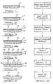
- FIGURES 1-7 are partial cross-sectional views which schematically illustrate sequential proce ssing steps according to the teachings of the preferred embodiment of the present invention.
- FIGURE 8 is a flow chart arranged so that the boxes therein generally relate to the steps performed on the substrate as illustrated in the adjacent FIGURES 1-7.
- thermosetting polymeric materials include epoxy, phenolic base materials, and polyimides.
- the dielectric substrate may be molded from the polymers and may contain fillers and/or reinforcing agents.
- Presently preferred substrates include glass reinforced epoxy resin materials.
- Suitable thermoplastic polymeric materials include polyolefins such as polypropylene, polysulfones, polycarbonates, and other suitable materials.
- the first general step as illustrated in FIGURE 1 is to apply a layer 12 of metallic seed particles onto the substrate 10.
- the seed particles are collodial particles of palladium and tin which are applied in the manner disclosed in the aforementioned US-A-4,448,804 to Amelio et al which is hereby incorporated by reference.
- a copper sheet is laminated to the substrate surface and the copper later etched away.
- the etched surface of the substrate is conditioned by bringing it into contact with an acidic solution containing a multi-functional cationic group containing at least two available cationic moities.
- the surface of the substrate is activated or seeded by bringing it into contact with at least one solution containing stannous and/or palladium chloride.
- the substrate is then rinsed with distilled water, with the activated surface being then brought into contact with an aqueous solution of HCL.
- the HCL treated surface is then rinsed with the de-ionized water.
- seed particles of palladium and tin are presently preferred, it is expected that seed particles selected from the periodic group of VIII, and IVA may also be used in accordance with the method of this invention. It should also be understood that a wide variety of different methods for seeding the substrate surface may also be used as should be apparent to the skilled practioner.
- the next general step is to apply a layer 14 of maskant, such as photoresist, onto the seeded substrate.
- the maskant layer 14 can be applied by a variety of methods such as by spin coating.
- the maskant layer takes the form of a negative photoresist film which is laminated onto the substrate surface.
- the next step is to selectively expose areas of the seeded substrate which are desired for conductor formation. These areas are schematically shown bearing reference numerals 16 and 18. This is conveniently accomplished by exposing the photoresist layer 14 through an appropriate mask. Through subsequent developing in a known manner, the negative of the desired pattern is produced in the photoresist layer 14. In the areas 16, 18 where the photoresist layer has been removed, the seeded or catalyzed regions of the substrate are exposed.
- the exposed seeded areas 16, 18 are next plated using conventional electroless plating techniques such as those disclosed in the mentioned US-A- 4,448,804.
- the plated copper is illustrated in FIGURE 4 as conductor lines 20 and 22. Electroless copper plating techniques are well known in the art and may be used in accordance with this invention. Preferably, the plating is done in two steps differing in the composition baths used and in the duration of the steps as more fully disclosed in the US-A-4,448,804 reference.
- the next step is to remove the photoresist layer 14. This is conventionally done by stripping the photoresist preferably with methylene chloride or a similar solvent which is selectively reactive with the developed photoresist.
- the seed particles are removed by subjecting the substrate to a gas plasma discharge designed to react with the particles.
- the plasma discharge step is shown schematically in FIGURE 6.
- the plasma discharge treatment is carried out in a batch process wherein a plurality of similarly processed substrates are placed in a holder in a reactor chamber.
- the reactor chamber includes an inlet for introducing gas into the chamber for producing the plasma therefrom.
- a source of radio frequency (RF) power provides the exciting energy to electrodes located in the reaction chamber.
- the RF power employed is between 0,02 and 0,1 watt per square centimeter of electrode area continuous radiation at a frequency in the megahertz range.
- the reactor and related equipment is commercially available from Branson International Plasma Corporation of Hayward, California.
- the gas introduced into the reaction chamber is preferably a mixture of oxygen and a halocarbon.
- suitable halocarbons include tetrafluoromethane (CF4) and chlorotrifluoromethane (CClF3) and related chlorofluoromethanes.
- the presently preferred plasma gas is a mixture of O2 and CF4 in the ration of 60 to 90 percent oxygen to halocarbon by volume.
- a flow of a mixture of 70 percent by volume oxygen and 30 percent by volume CF4 is established through the reactor chamber at a rate of about 1,0 to 4,0 standard liters per minute.
- the other end of the vacuum chamber is connected to a vacuum pump which maintains the pressure within the chamber at about 4.10 -6 bar.
- An RF frequency of about 13,5 megahertz is established to create a "cold" plasma therein.
- the substrates remain in the chamber for about 8 to 20 minutes, with 12 minutes being presently preferred. Then, the substrates are removed from the chamber.
- the exact processing parameters may be suitably varied in a manner which will be apparent to the skilled practioner having the benefit of the teachings of this patent.
- the percent by volume of oxygen should be no more than 90 % because of loss of conversion of atomic state.
- the pressure in the reactor should be between 0,13 and 0,53 Pa (1,3 . 10 ⁇ 6 and 5,3 . 10 ⁇ 6 bar) because of current reactor design limitations.
- the temperature in the reactor should be between 25°C and preferably no higher than 140°C because thermal degradation of polymeric substrates can occur at higher temperatures.
- the time that the substrate is exposed to the plasma should be 8 to 20 minutes to provide sufficient time for conversion from the metallic state to the ionic state and minimize material degradation. It is believed that the fluorine and oxygen containing radicals in the plasma will react with the palladium and tin seed particles to thereby form the salts thereof; namely: palladium fluoride and stannous fluoride and their oxides, respectively.
- the converted regions of the substrate are shown schematically in FIGURE 6 in the areas bearing reference numerals 30, 32 and 34. Some of the palladium and tin particles may be volatized and removed in the main gas stream to the vacuum pump.
- the final step as represented in FIGURE 7 is to wash the substrate in a solvent. It has been discovered that by washing the substrate in suitable alkaline or acidic solutions, the metallic seed particles are removed from the areas 30, 32 and 34 between the conductors 20, 22.
- suitable alkaline solvents include solutions of caustic soda, potassium hydroxide, and sodium silicate. Acidic solutions such as hydrochloric and nitric or sulfuric acids in proper strengths can be used. However, alkaline solvents are preferred because they will not attack the copper conductors 20, 22 but will selectively dissolve the salts of palladium and tin which were created during the plasma discharge step.
- the substrates can be washed by rinsing them in a bath containing a 5-50% by volume solution of caustic soda for about 3 minutes.
Description
- This invention relates to a method for making printed circuit boards and the like. More particularly, it involves a method of making circuit boards wherein conductor material is electrolessly deposited onto seeded areas on a dielectric substrate.
- In the manufacture of printed circuit boards and the like, a conductive circuit pattern is provided on at least one surface of a dielectric substrate. The conductor pattern can be formed on the substrate using a variety of known techniques. One of the better known techniques includes the electroless direct bond (EDB) technique where copper is electrolessly plated directly onto the surface of the substrate in the desired pattern. The conductor pattern may include conductor lines on the surface of the substrate as well as in holes (often referred to as plated through holes) which connect one or more conductive layers together. Since the dielectric substrate is non-conductive, it is generally necessary to seed or catalyze the substrate prior to deposition of the metal onto the substrate. Among the more widely employed procedures for seeding the substrate is to deposit colloidal particles of palladium (Pd) and tin (Sn) on the substrate. A copper metallic coating can then be applied to the seeded areas by way of well known electroless deposition techniques.
- EP-A-0153683 and US-A-4,448,804 disclose a particularly advantageous technique for making printed circuit boards and the like. Briefly, these documents disclose the steps of coating a previously seeded substrate with a maskant such as a photoresist. The photoresist is then developed leaving exposed those seeded areas which correspond to the desired conductor pattern. Copper is then electrolessly plated onto the substrate and the remaining photoresist is removed.
- While the process noted above has provided extremely satisfactory results, electrical shorts between the conductor lines on the substrate have been occasionally experienced. Of course, such problems are to be avoided if at all possible.
- The broad teachings of the present invention stem from the observation that the metallic seed particles that remain on the substrate surface may cause undesirable electrical shorting between the various conductor lines on the substrate. According to the teachings of this invention, once the maskant layer is removed during the aforementioned processing steps, the substrate is then subjected to a plasma discharge. The plasma is preferably produced from a mixture of gases which react with the metallic seed particles to aid in their removal. Preferably, the gas mixture includes oxygen and a halo-carbon where the metallic seed particles comprise palladium and tin. It is particularly advantageous that the plasma discharge step is followed by washing the substrate in a solvent.
- The present invention involves a method of making printed circuit boards which includes the steps of:
- a) applying metallic seed particules on a surface of a dielectric substrate;
- b) coating the substrate surface with a maskant layer;
- c) selectively removing portions of the maskant to expose seeded areas on the substrate desired for conductor formation;
- d) forming metallic conductors on the exposed seeded areas by electroless deposition;
- e) removing the remaining maskant; and is characterized by the subsequent steps of:
- f) subjecting the substrate to a plasma discharge; and
- g) washing the substrate in a solvent to remove the seed particles from the substrate.
- The various advantages of the present invention will become apparent to one skilled in the art upon reading the following specification and by reference to the drawings in which:
- FIGURES 1-7 are partial cross-sectional views which schematically illustrate sequential proce ssing steps according to the teachings of the preferred embodiment of the present invention; and
- FIGURE 8 is a flow chart arranged so that the boxes therein generally relate to the steps performed on the substrate as illustrated in the adjacent FIGURES 1-7.
- The method of the present invention is applicable to forming printed circuit patterns on a wide variety of dielectric substrates including thermoplastic and thermosetting resins, glass and ceramics. Typical thermosetting polymeric materials include epoxy, phenolic base materials, and polyimides. The dielectric substrate may be molded from the polymers and may contain fillers and/or reinforcing agents. Presently preferred substrates include glass reinforced epoxy resin materials. Suitable thermoplastic polymeric materials include polyolefins such as polypropylene, polysulfones, polycarbonates, and other suitable materials.
- The first general step as illustrated in FIGURE 1 is to apply a layer 12 of metallic seed particles onto the
substrate 10. Preferably, the seed particles are collodial particles of palladium and tin which are applied in the manner disclosed in the aforementioned US-A-4,448,804 to Amelio et al which is hereby incorporated by reference. Briefly, a copper sheet is laminated to the substrate surface and the copper later etched away. The etched surface of the substrate is conditioned by bringing it into contact with an acidic solution containing a multi-functional cationic group containing at least two available cationic moities. The surface of the substrate is activated or seeded by bringing it into contact with at least one solution containing stannous and/or palladium chloride. The substrate is then rinsed with distilled water, with the activated surface being then brought into contact with an aqueous solution of HCL. The HCL treated surface is then rinsed with the de-ionized water. - Although seed particles of palladium and tin are presently preferred, it is expected that seed particles selected from the periodic group of VIII, and IVA may also be used in accordance with the method of this invention. It should also be understood that a wide variety of different methods for seeding the substrate surface may also be used as should be apparent to the skilled practioner.
- The next general step (see FIGURE 2) is to apply a
layer 14 of maskant, such as photoresist, onto the seeded substrate. Themaskant layer 14 can be applied by a variety of methods such as by spin coating. Preferably, however, the maskant layer takes the form of a negative photoresist film which is laminated onto the substrate surface. - As shown in FIGURE 3, the next step is to selectively expose areas of the seeded substrate which are desired for conductor formation. These areas are schematically shown bearing
reference numerals 16 and 18. This is conveniently accomplished by exposing thephotoresist layer 14 through an appropriate mask. Through subsequent developing in a known manner, the negative of the desired pattern is produced in thephotoresist layer 14. In theareas 16, 18 where the photoresist layer has been removed, the seeded or catalyzed regions of the substrate are exposed. - The exposed seeded
areas 16, 18 are next plated using conventional electroless plating techniques such as those disclosed in the mentioned US-A- 4,448,804. The plated copper is illustrated in FIGURE 4 asconductor lines - As illustrated in FIGURE 5, the next step is to remove the
photoresist layer 14. This is conventionally done by stripping the photoresist preferably with methylene chloride or a similar solvent which is selectively reactive with the developed photoresist. - As can be seen in FIGURE 5, there unfortunately remains some seed particles in the
areas conductors conductors - The plasma discharge step is shown schematically in FIGURE 6. Preferably, the plasma discharge treatment is carried out in a batch process wherein a plurality of similarly processed substrates are placed in a holder in a reactor chamber. The reactor chamber includes an inlet for introducing gas into the chamber for producing the plasma therefrom. A source of radio frequency (RF) power provides the exciting energy to electrodes located in the reaction chamber. Typically, the RF power employed is between 0,02 and 0,1 watt per square centimeter of electrode area continuous radiation at a frequency in the megahertz range. By way of a non-limiting example, the reactor and related equipment is commercially available from Branson International Plasma Corporation of Hayward, California.
- The gas introduced into the reaction chamber (from which a plasma is produced from the RF energy), is preferably a mixture of oxygen and a halocarbon. Where the seed particles are palladium and tin, suitable halocarbons include tetrafluoromethane (CF₄) and chlorotrifluoromethane (CClF₃) and related chlorofluoromethanes. The presently preferred plasma gas is a mixture of O₂ and CF₄ in the ration of 60 to 90 percent oxygen to halocarbon by volume.
- By way of a specific example, a flow of a mixture of 70 percent by volume oxygen and 30 percent by volume CF₄ is established through the reactor chamber at a rate of about 1,0 to 4,0 standard liters per minute. The other end of the vacuum chamber is connected to a vacuum pump which maintains the pressure within the chamber at about 4.10 -6 bar. An RF frequency of about 13,5 megahertz is established to create a "cold" plasma therein. The substrates remain in the chamber for about 8 to 20 minutes, with 12 minutes being presently preferred. Then, the substrates are removed from the chamber.
- The exact processing parameters may be suitably varied in a manner which will be apparent to the skilled practioner having the benefit of the teachings of this patent. However, it is believed that the percent by volume of oxygen should be no more than 90 % because of loss of conversion of atomic state. On the other hand, it should be no less than 60 % because of reduced reaction rates. The pressure in the reactor should be between 0,13 and 0,53 Pa (1,3 . 10⁻⁶ and 5,3 . 10⁻⁶ bar) because of current reactor design limitations. The temperature in the reactor should be between 25°C and preferably no higher than 140°C because thermal degradation of polymeric substrates can occur at higher temperatures. The time that the substrate is exposed to the plasma should be 8 to 20 minutes to provide sufficient time for conversion from the metallic state to the ionic state and minimize material degradation. It is believed that the fluorine and oxygen containing radicals in the plasma will react with the palladium and tin seed particles to thereby form the salts thereof; namely: palladium fluoride and stannous fluoride and their oxides, respectively. The converted regions of the substrate are shown schematically in FIGURE 6 in the areas bearing
reference numerals 30, 32 and 34. Some of the palladium and tin particles may be volatized and removed in the main gas stream to the vacuum pump. - The final step as represented in FIGURE 7 is to wash the substrate in a solvent. It has been discovered that by washing the substrate in suitable alkaline or acidic solutions, the metallic seed particles are removed from the
areas 30, 32 and 34 between theconductors copper conductors - In view of the foregoing, those skilled in the art can appreciate that the present invention provides significant advantages in removing seed particles from the surfaces of circuit board substrates. While this invention has been described in connection with a particular example thereof, various other modifications will become apparent to the skilled practioner upon a study of the specification, drawings and following claims.
Claims (6)
- Method for making printed circuit boards, including the steps of:a) applying metallic seed particles (12) onto a surface of a dielectric substrate (10);b) applying a maskant layer (14) onto said substrate surface over the seed particles (12);c) selectively removing portions of the maskant layer (14) to expose seeded areas (16, 18) on the substrate desired for conductor formation;d) electrolessly depositing metallic conductors (20, 22) on the exposed seeded areas (16, 18) on the substrate;e) removing the remaining maskant (14); characterized by the subsequent steps of:f) subjecting the substrate surface to a plasma discharge; andg) washing the substrate in a solvent to remove seed particles (30, 32, 34) from the substrate surface.
- Method in accordance with Claim 1, characterized in that the seed particles (12) comprise palladium and tin, and that the plasma is produced from a gaseous mixture of oxygen and a halocarbon.
- Method in accordance with Claim 1, characterized in that the solvent is an alkaline solvent.
- Method in accordance with Claim 4, characterized in that the alkaline solvent is selected from the group of caustic soda, potassium hydroxide and sodium silicate.
- Method in accordance with claim 1, characterized by the steps of:a) depositing collodial seed particles (12) of palladium and tin onto a surface of an epoxy resin substrate (10);b) coating the seeded substrate surface by laminating a photoresist foil (14) onto the surface;c) selectively removing portions of the photoresist to expose seeded areas (16, 18) on the substrate desired for conductor formation;d) electrolessly depositing copper onto the exposed seeded areas (16, 18) to thereby form electrical conductors (20, 22) on the substrate surface;e) removing remaining portions of the photoresist (14);f) exposing the substrate to a gaseous plasma formed in a radio frequency field from a mixture consisting of oxygen and a halocarbon for a sufficient period of time to convert the palladium and tin seed particles (30, 32, 34) into their respective salt forms; andg) washing the substrate in a solvent to remove the seed particles (30, 32, 34) that have been converted to their salt forms by said plasma.
- Method in accordance with Claims 2 or 5, characterized in that the halocarbon is selected from the group of tetrafluoromethane (CF₄) and chlorotrifluoromethane (CClF₃).
Applications Claiming Priority (2)
| Application Number | Priority Date | Filing Date | Title |
|---|---|---|---|
| US822216 | 1986-01-24 | ||
| US06/822,216 US4718972A (en) | 1986-01-24 | 1986-01-24 | Method of removing seed particles from circuit board substrate surface |
Publications (3)
| Publication Number | Publication Date |
|---|---|
| EP0231795A2 EP0231795A2 (en) | 1987-08-12 |
| EP0231795A3 EP0231795A3 (en) | 1988-04-20 |
| EP0231795B1 true EP0231795B1 (en) | 1991-04-24 |
Family
ID=25235478
Family Applications (1)
| Application Number | Title | Priority Date | Filing Date |
|---|---|---|---|
| EP87100547A Expired - Lifetime EP0231795B1 (en) | 1986-01-24 | 1987-01-16 | Method for making printed circuit boards |
Country Status (4)
| Country | Link |
|---|---|
| US (1) | US4718972A (en) |
| EP (1) | EP0231795B1 (en) |
| JP (1) | JPS62179197A (en) |
| DE (1) | DE3769484D1 (en) |
Families Citing this family (19)
| Publication number | Priority date | Publication date | Assignee | Title |
|---|---|---|---|---|
| GB8728399D0 (en) * | 1987-12-04 | 1988-01-13 | Secretary Trade Ind Brit | Deposition of materials to substrates |
| US5092957A (en) * | 1989-11-24 | 1992-03-03 | The United States Of America As Represented By The United States Department Of Energy | Carrier-lifetime-controlled selective etching process for semiconductors using photochemical etching |
| US5077176A (en) * | 1990-07-30 | 1991-12-31 | At&T Bell Laboratories | Pre-plate cleaning process |
| US5167992A (en) * | 1991-03-11 | 1992-12-01 | Microelectronics And Computer Technology Corporation | Selective electroless plating process for metal conductors |
| US5919514A (en) * | 1992-12-28 | 1999-07-06 | Xerox Corporation | Process for preparing electroded donor rolls |
| US5509557A (en) * | 1994-01-24 | 1996-04-23 | International Business Machines Corporation | Depositing a conductive metal onto a substrate |
| US5487218A (en) * | 1994-11-21 | 1996-01-30 | International Business Machines Corporation | Method for making printed circuit boards with selectivity filled plated through holes |
| US6544584B1 (en) * | 1997-03-07 | 2003-04-08 | International Business Machines Corporation | Process for removal of undesirable conductive material on a circuitized substrate and resultant circuitized substrate |
| US7381356B2 (en) | 2003-10-02 | 2008-06-03 | Kikusui Seisakusho, Ltd. | Rotary powder compression molding machine |
| WO2008090418A1 (en) * | 2007-01-22 | 2008-07-31 | Freescale Semiconductor, Inc. | Liquid cleaning composition and method for cleaning semiconductor devices |
| EP2003939A1 (en) * | 2007-06-14 | 2008-12-17 | Nederlandse Organisatie voor toegepast- natuurwetenschappelijk onderzoek TNO | Method for preparing a pattern for a 3-dimensional electric circuit |
| EP2197253A1 (en) * | 2008-12-12 | 2010-06-16 | Nederlandse Organisatie voor toegepast-natuurwetenschappelijk Onderzoek TNO | Method for electric circuit deposition |
| EP2281921A1 (en) | 2009-07-30 | 2011-02-09 | Nederlandse Organisatie voor toegepast -natuurwetenschappelijk onderzoek TNO | Apparatus and method for atomic layer deposition. |
| JP5573429B2 (en) * | 2009-08-10 | 2014-08-20 | 住友ベークライト株式会社 | Electroless nickel-palladium-gold plating method, plated product, printed wiring board, interposer, and semiconductor device |
| EP2360293A1 (en) | 2010-02-11 | 2011-08-24 | Nederlandse Organisatie voor toegepast -natuurwetenschappelijk onderzoek TNO | Method and apparatus for depositing atomic layers on a substrate |
| EP2362002A1 (en) | 2010-02-18 | 2011-08-31 | Nederlandse Organisatie voor toegepast -natuurwetenschappelijk onderzoek TNO | Continuous patterned layer deposition |
| EP2362411A1 (en) | 2010-02-26 | 2011-08-31 | Nederlandse Organisatie voor toegepast -natuurwetenschappelijk onderzoek TNO | Apparatus and method for reactive ion etching |
| EP3085212A4 (en) * | 2013-12-17 | 2017-11-22 | Sanmina Corporation | Methods of forming segmented vias for printed circuit boards |
| CN107710889B (en) * | 2015-05-06 | 2021-06-29 | 哈钦森技术股份有限公司 | Plasma treatment of flexures for hard disk drives |
Citations (1)
| Publication number | Priority date | Publication date | Assignee | Title |
|---|---|---|---|---|
| US4448804A (en) * | 1983-10-11 | 1984-05-15 | International Business Machines Corporation | Method for selective electroless plating of copper onto a non-conductive substrate surface |
Family Cites Families (17)
| Publication number | Priority date | Publication date | Assignee | Title |
|---|---|---|---|---|
| US30505A (en) * | 1860-10-23 | Fukntture-caster | ||
| SE332214B (en) * | 1968-07-12 | 1971-02-01 | Gylling & Co | |
| US3867216A (en) * | 1972-05-12 | 1975-02-18 | Adir Jacob | Process and material for manufacturing semiconductor devices |
| US3971684A (en) * | 1973-12-03 | 1976-07-27 | Hewlett-Packard Company | Etching thin film circuits and semiconductor chips |
| JPS5091760A (en) * | 1973-12-18 | 1975-07-22 | ||
| JPS5320896A (en) * | 1976-08-11 | 1978-02-25 | Seiko Epson Corp | Manufacture of liquid crystal display element |
| US4253907A (en) * | 1979-03-28 | 1981-03-03 | Western Electric Company, Inc. | Anisotropic plasma etching |
| JPS5727177A (en) * | 1980-07-25 | 1982-02-13 | Yamamoto Yogyo Kako Kk | Method for finishing ornamental wall representing pattern of natural stone |
| DE3110415C2 (en) * | 1981-03-18 | 1983-08-18 | Ruwel-Werke Spezialfabrik für Leiterplatten GmbH, 4170 Geldern | Process for the manufacture of printed circuit boards |
| US4478883A (en) * | 1982-07-14 | 1984-10-23 | International Business Machines Corporation | Conditioning of a substrate for electroless direct bond plating in holes and on surfaces of a substrate |
| US4416725A (en) * | 1982-12-30 | 1983-11-22 | International Business Machines Corporation | Copper texturing process |
| JPS6074599A (en) * | 1983-09-30 | 1985-04-26 | 株式会社日立製作所 | Printed circuit board and method of producing same |
| US4554182A (en) * | 1983-10-11 | 1985-11-19 | International Business Machines Corporation | Method for conditioning a surface of a dielectric substrate for electroless plating |
| JPS60147395A (en) * | 1984-01-12 | 1985-08-03 | Fuji Photo Film Co Ltd | Plate surface cleaning agent for planographic plate |
| DE3407114A1 (en) * | 1984-02-28 | 1985-09-05 | Bayer Ag, 5090 Leverkusen | METHOD FOR THE PRODUCTION OF CIRCUIT BOARDS |
| US4555303A (en) * | 1984-10-02 | 1985-11-26 | Motorola, Inc. | Oxidation of material in high pressure oxygen plasma |
| US4568562A (en) * | 1984-11-28 | 1986-02-04 | General Dynamics, Pomona Division | Method of electroless plating employing plasma treatment |
-
1986
- 1986-01-24 US US06/822,216 patent/US4718972A/en not_active Expired - Fee Related
- 1986-11-28 JP JP61282227A patent/JPS62179197A/en active Granted
-
1987
- 1987-01-16 EP EP87100547A patent/EP0231795B1/en not_active Expired - Lifetime
- 1987-01-16 DE DE8787100547T patent/DE3769484D1/en not_active Expired - Fee Related
Patent Citations (1)
| Publication number | Priority date | Publication date | Assignee | Title |
|---|---|---|---|---|
| US4448804A (en) * | 1983-10-11 | 1984-05-15 | International Business Machines Corporation | Method for selective electroless plating of copper onto a non-conductive substrate surface |
Also Published As
| Publication number | Publication date |
|---|---|
| JPS62179197A (en) | 1987-08-06 |
| EP0231795A2 (en) | 1987-08-12 |
| DE3769484D1 (en) | 1991-05-29 |
| US4718972A (en) | 1988-01-12 |
| JPH0317390B2 (en) | 1991-03-07 |
| EP0231795A3 (en) | 1988-04-20 |
Similar Documents
| Publication | Publication Date | Title |
|---|---|---|
| EP0231795B1 (en) | Method for making printed circuit boards | |
| US4597988A (en) | Process for preparing printed circuit board thru-holes | |
| US20120107522A1 (en) | Method for producing formed circuit component | |
| US4834835A (en) | Producing viaholes in plastic sheets and application of the method | |
| US4430154A (en) | Method of producing printed circuit boards | |
| EP0331684A1 (en) | Process for fabricating multilayer circuit boards | |
| US5639389A (en) | Process for the production of structures | |
| US4756930A (en) | Process for preparing printed circuit board thru-holes | |
| US4351697A (en) | Printed wiring boards | |
| JPH01259170A (en) | Production of metal structure on insulator | |
| US4711822A (en) | Metal core printed circuit boards | |
| EP0248029B1 (en) | Method for selectively removing adhesives from polyimide substrates | |
| US5092967A (en) | Process for forming printed circuits | |
| US6758984B2 (en) | Selective removal of dielectric materials and plating process using same | |
| KR100216328B1 (en) | Method for direct metallization of conductive boards | |
| JPH03170680A (en) | Direct metal covering of nonconductive supporting body | |
| JPH10209607A (en) | Manufacture of circuit board | |
| US4849302A (en) | Electrolytically metallized article and processes therefore | |
| KR100763349B1 (en) | Method for manufacturing metal stamp | |
| JPH08134639A (en) | Surface treatment of resin | |
| GB2243618A (en) | Electroforming mandrel; making continuously electroformed thickness modulated or perforated metal foil | |
| JPH04229694A (en) | Method of improving fusion of metal to polyimide surface | |
| JP3843686B2 (en) | Circuit board manufacturing method | |
| CA1202734A (en) | Process for preparing printed circuit board thru- holes | |
| JP2005281762A (en) | Electroless plating method |
Legal Events
| Date | Code | Title | Description |
|---|---|---|---|
| PUAI | Public reference made under article 153(3) epc to a published international application that has entered the european phase |
Free format text: ORIGINAL CODE: 0009012 |
|
| AK | Designated contracting states |
Kind code of ref document: A2 Designated state(s): DE FR GB |
|
| 17P | Request for examination filed |
Effective date: 19871202 |
|
| PUAL | Search report despatched |
Free format text: ORIGINAL CODE: 0009013 |
|
| AK | Designated contracting states |
Kind code of ref document: A3 Designated state(s): DE FR GB |
|
| 17Q | First examination report despatched |
Effective date: 19900406 |
|
| GRAA | (expected) grant |
Free format text: ORIGINAL CODE: 0009210 |
|
| AK | Designated contracting states |
Kind code of ref document: B1 Designated state(s): DE FR GB |
|
| REF | Corresponds to: |
Ref document number: 3769484 Country of ref document: DE Date of ref document: 19910529 |
|
| ET | Fr: translation filed | ||
| PLBE | No opposition filed within time limit |
Free format text: ORIGINAL CODE: 0009261 |
|
| STAA | Information on the status of an ep patent application or granted ep patent |
Free format text: STATUS: NO OPPOSITION FILED WITHIN TIME LIMIT |
|
| 26N | No opposition filed | ||
| PGFP | Annual fee paid to national office [announced via postgrant information from national office to epo] |
Ref country code: GB Payment date: 19951215 Year of fee payment: 10 |
|
| PGFP | Annual fee paid to national office [announced via postgrant information from national office to epo] |
Ref country code: FR Payment date: 19960103 Year of fee payment: 10 |
|
| PGFP | Annual fee paid to national office [announced via postgrant information from national office to epo] |
Ref country code: DE Payment date: 19960126 Year of fee payment: 10 |
|
| PG25 | Lapsed in a contracting state [announced via postgrant information from national office to epo] |
Ref country code: GB Effective date: 19970116 |
|
| GBPC | Gb: european patent ceased through non-payment of renewal fee |
Effective date: 19970116 |
|
| PG25 | Lapsed in a contracting state [announced via postgrant information from national office to epo] |
Ref country code: FR Effective date: 19970930 |
|
| PG25 | Lapsed in a contracting state [announced via postgrant information from national office to epo] |
Ref country code: DE Effective date: 19971001 |
|
| REG | Reference to a national code |
Ref country code: FR Ref legal event code: ST |