EP0237365B1 - Photo-sensitive device - Google Patents
Photo-sensitive device Download PDFInfo
- Publication number
- EP0237365B1 EP0237365B1 EP87400099A EP87400099A EP0237365B1 EP 0237365 B1 EP0237365 B1 EP 0237365B1 EP 87400099 A EP87400099 A EP 87400099A EP 87400099 A EP87400099 A EP 87400099A EP 0237365 B1 EP0237365 B1 EP 0237365B1
- Authority
- EP
- European Patent Office
- Prior art keywords
- reading
- read
- switches
- row
- potential
- Prior art date
- Legal status (The legal status is an assumption and is not a legal conclusion. Google has not performed a legal analysis and makes no representation as to the accuracy of the status listed.)
- Expired - Lifetime
Links
Images


Classifications
-
- H—ELECTRICITY
- H04—ELECTRIC COMMUNICATION TECHNIQUE
- H04N—PICTORIAL COMMUNICATION, e.g. TELEVISION
- H04N25/00—Circuitry of solid-state image sensors [SSIS]; Control thereof
- H04N25/70—SSIS architectures; Circuits associated therewith
- H04N25/76—Addressed sensors, e.g. MOS or CMOS sensors
Definitions
- the present invention relates to a photosensitive device in the solid state.
- the present invention relates to a photosensitive device which can be used for the detection of visible radiation as well as X-rays or any other type of radiation.
- a scintillator made of gadolinium oxide for example, so as to convert the X-radiation into visible radiation detected by photodiodes.
- the detectors can also be produced in any semiconductor that is known to be produced with a thickness sufficient to ensure direct detection of X-rays.
- the device according to the invention can only be used if there is a signal illumination phase and a reading phase of the device which are separated in time.
- the switches mounted in series in the photosensitive elements make it possible to disconnect each line of photosensitive elements from the columns when the other lines of the device are read.
- the photosensitive elements of a line which is not read do not inject their current of darkness into the columns when reading other lines.
- the reading of a line is not disturbed by the other lines which are not read. We remove the "diaphotie" and the "smearing".
- FIG. 1 represents the diagram of an embodiment of the photosensitive device according to the invention.
- This device comprises a photosensitive matrix 1 comprising a network of horizontal connections or lines and a network of vertical connections or columns.
- FIG. 1 only a 2x2 matrix has been shown to explain the operation of the device, with two rows Lp and Lp +1 and two columns Ci and C 2 .
- the lines and the columns cross, without being of course in contact, and a photosensitive element connects each line and each column which cross.
- each photosensitive element consists of the series connection of a capacitor G, of a photodiode D, made of amorphous silicon for example, and of an electronic switch I.
- the invention applies regardless of the respective position of the components forming part of the photosensitive element.
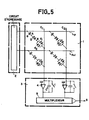
- the device of FIG. 1 also includes an addressing circuit 2, the outputs of which are connected to the rows of the matrix, and a reading and multiplexing circuit 3, the inputs of which are connected to the columns of the matrix.
- FIG. 1 shows an embodiment of the reading and multiplexing circuit 3 in which each column of the matrix is connected to the negative input of an operational amplifier 4 whose positive input is at a constant voltage which may be the mass of the device.
- These amplifiers are mounted as integrators and have a capacitance C 'connected between their negative input and their output.
- a switch i is mounted in parallel on each capacitor C 'to ensure its reset.
- the outputs of the amplifiers are connected to a multiplexer 5, of the network of switches or CCD type for example, the output of which supplies the output signal S of the device.
- the operational amplifiers mounted as integrators copy the polarization of their positive input on their negative input.
- the positive input of the amplifiers is at a constant voltage, for example at the ground of the device.
- These amplifiers therefore connect the columns which are connected to their negative input to ground.
- a photosensitive element of the device of Figure 1 for example the element located at the intersection of the column Ci and the p th line Lp of the matrix.
- a voltage pulse V P1 is applied to all of the rows of the matrix via the addressing circuit.
- the amplitude of signal Vp goes from 0 to Vp l and at time t 2 , the amplitude of signal Vp goes from V P1 to O.
- the voltage at point A follows, after charging the capacity G, the voltage variation occurring on the lines, that is to say that from the instant ti, VA increases then stabilizes at the value V c which is the elbow or threshold voltage of the photodiode D, which directly polarizes the diode D, the cathode of which is connected to ground by the switch 1 which is on.
- any type of photodiode D can be used, for example a PIN, PN or Schottky type photodiode.
- the arrival of the pulse V P1 causes the circulation of a current corresponding to a charge Qi - Figure 2e.
- V P1 returns to zero and the voltage VA becomes negative and equal to where C G is the value of the capacitance G and where C D represents the capacitance of the photodiode D.
- C G 10 C D.
- the photodiode then works in vidicon mode and will be able to detect the light. It generates from time t 2 a dark current I OBS1 of which a fraction equal to is injected into the column.
- the device receives the light signal to be analyzed h s.
- the application of this light flash has been represented symbolically in FIG. 2a.
- This flash creates a photocurrent in photodiode D which will tend to return to zero voltage.
- the voltage VA increases slightly from ts.
- Q the amount of charge created and separated in photodiode D. The fraction is injected into the column.
- Photodiode D generates a dark current I OBS2 which is no longer injected into the column but which accumulates at point B.
- the potential of point B begins to decrease with a slope equal to I OBS2 / C D.
- the maximum charge it can store is 2Vc.CD.
- the potential of point A as a first approximation remains constant.
- This phase 0 6 marks the beginning of the reading of the line Lp.
- Point B is again connected to ground and then injects into the column a quantity of charges Q 6 corresponding to the fraction of the charge of darkness stored by point B during phase 5.
- Vp 2 of amplitude greater than that of V P1 is applied to the p th line and to it alone.
- the potential of point A increases and stabilizes at V c when photodiode D conducts. Due to the directing of photodiode D, there is circulation of a quantity of charge Q 7 of sign opposite to that of charges Q 2 , Q 3 , Q 4 , Q 6 and of the same sign as Qi and Qs .
- the charge quantity Q7 contains the signal information in the same way as Q 3 . It should be noted that Q 3 cannot be used because the light flash is sent simultaneously to the entire device and all the photodiodes flow simultaneously on the columns which provide the average value of the light signal applied.
- the signal information will be obtained from the load Q 7 .
- the device according to the invention comprises photosensitive elements each having a capacity, a photodiode and a switch. There is therefore no direct current flowing through the photosensitive elements.
- the fraction of the dark current I OBS2 equal to which is injected at the instant ts in the form of the charge Q 6 and which corresponds to the accumulation of the dark current from t 5 to ts while the lines Li to Lp- 1 were being read.
- This current is poured out at time t 7 and is compensated for by making the sum Q 6 + Q 7 .
- the reading and multiplexing circuit reads each photodiode of the selected line by summing the charges which circulate, starting before the switches of the selected line are closed and ending while the pulse Vp 2 is applied to the selected line.
- the sum Q 6 + Q7 shows that it only intervenes during phase 3 corresponding to signal illumination and during safety phases 2 and 4, the duration of which may be short compared to that of phase 5.
- V P2 of amplitude greater than V P1 displaces the average value of the point of polarization of the photodiode in direct in a zone where its dynamic resistance is weaker, and thus accelerates the phenomenon of return towards the value of balance.
- Phase 6 can be deleted.
- the quantity of charge which circulates when the line voltage changes to V P2 is then equal to Qs + Q 7 .
- the switches are closed simultaneously with the transition to V P2 .
- V P2 returns to zero.
- VA voltage
- the reading and multiplexing circuit ensures the reading of each photodiode of the selected line by summing the charges which circulate starting before the switches of the selected line are closed, continuing while the pulse V P2 is applied to the selected line, and ending while the V P2 pulse has returned to zero.
- the P th line is read by opening the switch i on the feedback of the integrating amplifiers just before phase 6. The summation of the charges is then started. The charges can be read using the muliplexer, when the integrating amplifiers have summed the charges Q 6 + Q 7 or Q 6 + Q 7 + Q 8 or Q 6 + Q 7 + Q 8 + Q 9 . Then, the switches i are closed, so as to reset the capacities of the integrators to zero before the arrival of the charges coming from the line p + 1.
- the entire device is generally illuminated simultaneously, so we have to choose an average value for Qa and for Q 9 .
- Phase 11 is called the photodiodes reset phase.
- the scintillator placed in front of the device is opaque, the rear face of the panel can be lit.
- the substrate on which the photosensitive device is made must therefore be transparent.
- the quantity of charges Q 11 can also be produced by applying a voltage pulse to the lines which pushes the photodiodes D in reverse beyond their breakdown voltage, while remaining within the limits of reversible breakdown, so as to cause circulation. of a quantity of charges Q 11 sufficient to satisfy the inequality cited above in the case of a reset by optical means.
- Phase 12 is a phase that separates an imaging cycle from the following cycle. There is circulation of a quantity of charge Qi 2 .
- phase 1 begins with the application of a voltage pulse V P1 to all the lines of the device.
- the charge Q 1 which circulates evacuates the excess of charges which could have been provided during phase 11. It is therefore not necessary to precisely calibrate this charge Q 11 .
- the switches can be left open. Current accumulates at point B. It is then necessary to close the switches before reading of the device begins to authorize the signal charges to be discharged on the rows and the columns.
- the switches of the device must be closed during phases 0 1 and 0 4, while during phases 0 2 and 0 3 , they can be either open or closed.
- the switches of the device can be closed or open either during phases les 10 to ⁇ 12 .
- the preferred solution is to leave the switches closed during phases 10, 11 and 12, and even from phase 10 to the end of phase 4 of the following imaging cycle.
- switches I can be used in series in each photosensitive element.
- FIG. 4 represents an embodiment where each switch I is constituted by a transistor T.
- a transistor T One can use for example a TFT in amorphous silicon, a MOSFET or a JFET.
- each switch consists of two diodes mounted head to tail, di and d 2 .
- the capacitance C D of the photodiode must be much greater than the sum of the capacitances C d i and C d2 of the two diodes.
- Vc threshold voltage
- the switch is closed, while it is open for voltages higher than + Vc and lower than - Vc.
- this switch is controlled by modulating the potential of the lines of 2Vc.
- the diodes di and d 2 have a constant capacity as a function of the voltage V, when the latter is less than Vc, as shown in FIG. 3b.
- diodes d 1 and d 2 are PIN diodes.
- FIG. 6 represents the timing diagram of the device of FIG. 5, the operation of which is little different from that of FIG. 1.
- Diode d 1 and photodiode D are forward biased by voltage V P1 . Consequently, during the application of the voltage V P1 , the voltage VA is fixed at 2Vc and the voltage V B at Vc, if it is assumed that Vc is the threshold voltage of the diodes D, di and d 2 .
- a voltage equal to 2Vc is sent to the lines.
- the voltage VA remains substantially constant but undergoes an increase of 2Vc at time ts.
- the voltage V B goes to + Vc at time t 5 to then decrease, with a slope equal to I OBS2 / CD .
- the switches of the line Lp are closed by bringing the potential of this line to zero.
- the potential V B is fixed at - Vc.
- the voltage VA stabilizes at 2Vc and the voltage V B at Vc.
- Point B varies from 2Vc and goes to - Vc and point A varies from from 2Vc.
- This capacity can be moderate and allows the design of a relatively simple reading and multiplexing circuit.
- this device does not require, as when the switches are constituted by transistors, an additional network of lines to control the transistors.
- Figures 7, 8a, b and c, and 9 relate to a technological embodiment of the device of Figure 5, and more particularly of a photosensitive element of this device.
- Figure 7 is a top view of the photosensitive element thus produced, and Figures 8a to c are sectional views along the planes AA ', BB' and CC ' of this device.
- the transparent substrate on which the photosensitive elements are made is designated by the reference 6.
- This substrate carries a first conductive level 7 which is used to make the columns, the contact with the columns of the diode di - figure 8a - and the contact at point B of the diode D with the diodes di and d 2 - figures 8a and b.
- the first conductive level 7 In the case where the optical reset is carried out through the substrate, the first conductive level 7 must be transparent.
- a PIN layer is deposited and etched so as to produce the diodes di, d 2 and D.
- the diodes d i and d 2 and D are delimited by dotted lines.
- An insulating layer 8 is deposited which serves in the part where it covers the diode D to constitute the capacitor G and which also serves to isolate the passage from the second conductive level 9.
- the following four contacts are opened: a contact on d i , figure 8a - a contact on d 2 , figure 8b - a contact on the column to connect d 2 - a contact on the contact located under the diode D to connect the diode d i to the diode D.
- the second conductive level 9 is deposited and etched to connect the diode di to point B - figure 8a, to connect the diode d 2 to the column - figure 8b and to make the lines.
- This second conducting level 9 must be transparent to the light radiation to be analyzed.
- FIG. 8c it can be seen that a photosensitive element such as those represented in FIG. 5 has not been produced exactly, but a photosensitive element such as that represented in FIG. 9.
- each photosensitive element constituted by the series connection of a capacitance G, of a diode D and of two diodes d i and d 2 mounted head to tail, a capacitance G 'in series with a diode D '.
- the capacity of the assembly constituted by the capacity G ′ and the diode D ′ in series is less than or equal to the capacity that a simple insulator would have presented.
- the probability of fault by short-circuit is lower due to the diode D 'which is reverse biased if the capacitance G' is in short-circuit.
- switches 1 in FIG. 1 could be constituted by a transistor or by two diodes mounted head to tail.
- the switches 1 can also consist of multi-layer elements of the NIN or PIP type.
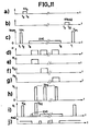
- FIG. 10 represents an embodiment of the addressing circuit for lines 2 which is represented in FIGS. 1, 4 and 5.
- This circuit comprises a logic shift register 11, controlled by at least one clock H.
- this register comprises six outputs Ri to Rs.
- Transistors h to Is are controlled by the outputs Ri to Rs and connected between a voltage V 1 and an output of the addressing circuit Si to Ss. Between each output of the circuit and a voltage Vcom, a King resistor is connected to Ro5 which imposes the voltage Vcom on the outputs of the circuit connected to lines that are not read.
- FIG. 11 is a timing diagram relating to the device of FIG. 10.
- Figure 11a concerns signal illumination.
- the light signal to be analyzed hvs which is applied between the instants ts and t 4 has been represented symbolically.
- V com is shown in FIG. 11 c.
- This voltage V com is made up of the different voltages to be applied to the lines when they are not read.
- the voltage V com comprises a voltage pulse Vpi from ti to t 2 , and a voltage equal to 2Vc from t 4 to ts. During the rest of the time, the voltage Vcom is at zero, that is to say to ground.
- FIG. 11 d shows the clock signal H of the shift register 11 of FIG. 10.
- FIGS. 11e, f and g show that each clock pulse of the signal H causes the output of the register to go high.
- Figure 11h shows the signal Vi.
- This signal Vi is formed by the different voltages to be applied to a line to read it.
- This signal Vi is at level O, and while one of the outputs of the register Ri, R 2 ... R 5 goes high, the signal V i generates a voltage pulse V P2 .
- FIG. 11 i the voltages are shown on the output Si which controls the line Li of the device.
- the transistor I 1 As long as the signal Ri is not at the high level, the transistor I 1 is blocked and the restoring resistance imposes the voltage Vcom on the output Si. It can be seen in FIG. 11 i that as long as the signal Ri is at the low level , the voltage V c om is imposed on the output Si. When the signal Ri is at the high level, the voltage Vi is found on the output Si.
- a transistor Ji to J 5 in parallel on the restoring resistors.
- the transistors J i to Js are of the same type as the transistors I 1 to I s but they are controlled by the following output of the register.
- the transistor Ji is controlled by the output R 2
- the transistor J 2 is controlled by the output Ra ...
- transistors I 1 to I 5 and J i to J s of the same type but by controlling the transistors J 1 to J s by the complementary outputs of the register.
- the transistor I 1 is controlled by the output Ri and the transistor J i by the complementary output R 1 and so on.
- transistors I 1 to I 5 and J 1 to J s which are complementary.
- the transistors I 1 and J 1 are controlled by the same output of the register, the same for the transistors 1 2 and J 2 ...
- the transistor 1 1 is passing, while the transistor Ji is blocked.
- the transistors used can be MOS transistors or TFT for example.
- FIG. 11j represents the control signal of the switches i ensuring the reset to zero when the capacities C ′ linked to the operational amplifiers 4 are high.
- the voltages delivered by the addressing circuit are defined to within a constant due to the capacitance G which is part of each photosensitive element.
- point B decreases with a slope equal to I OBS2 / C D from + Vc in the case of a switch constituted by two diodes mounted head to tail.
- the maximum charge that point B can store is equal to 2Vc Co, after which point B is at - Vc and the switch I is closed.
- the voltage V com is constituted by an increasing ramp of slope I mean OBS2 / C D , I mean OBS2 being an average value of the current I OBS2 .
- This ramp starts from + Vc at time t 4 so as to bring point B to zero at time t 4 .
- point B is at - V c at time t 4 .
- Figure 12d is similar to Figure 11d, but Figure 12e which represents the signal V 1 differs from Figure 11 h because between two voltage pulses Vp 2 the voltage does not return to zero.
- the voltage pulses V P2 are carried by a ramp which starts from zero at time t 4 and then increases with a slope equal to I mean OBS2 / C D.
- FIG. 12f shows the signal of the output S 2 of the addressing circuit of FIG. 10.
- the signal Vi is found on the output S 2 .
- the signal V com is at again applied to output S 2 .
- the use of a signal Vi such as that of FIG. 12e makes it possible to reduce the offset when passing from the voltage Vi to the voltage V co m. Now the voltage V com is calculated so that point B is close to zero.
- the signal Vi is superimposed on a ramp which starts from O whereas the signal Vcom is superimposed on a ramp which starts from V c so that there is a voltage offset at tg allowing the return of point B from Vc to zero .
- Figures 12g and 12h show the voltages VA and V B at two points A and B of the line controlled by the output S 2 .
- Vcom signals Vcom signals
- the voltages Vcom and Vi are carried by an increasing ramp of slope equal to I mean OBS2 / Co, where I mean OBS2 is an average value of the dark current of the photodiodes, so as to bring the point B to an average zero voltage.
- FIGS. 1 and 2 We have seen in the description of FIGS. 1 and 2 an embodiment of the reading and multiplexing circuit 3.
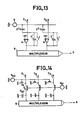
- FIG. 13 shows an embodiment in which the negative inputs of the amplifiers are connected via a capacitor C "to a generator G providing a compensation signal which makes it possible to adjust the average voltage at the output of the amplifiers 4.
- this circuit is used to generate the different voltages to be applied to the lines which are not read.
- This voltage shown in FIG. 11 c is called V com .
- This signal Vcom is applied to the positive input of amplifiers 4. It is known that these amplifiers copy the voltage existing on their positive input on their negative input.
- the addressing circuit provides a constant voltage, which can be equal to the mass, except during the time intervals where it provides the voltages to be applied to the lines to be read. In the embodiments of the addressing circuit of FIGS. 10 and 11, it is then necessary to replace the voltage V com by a constant voltage which can be the mass of the device.
- FIG. 14 represents a particular embodiment of the addressing and multiplexing circuit 3.
- FIG. 15 represents the timing diagram of the device of FIG. 14.
- This embodiment eliminates the use of operational amplifiers which are bulky and consume a lot of current.
- Figures 15a to h there is shown a series of elements of the device of Figure 14, that is to say a transistor T R , then a transistor T c and a capacitor C ST .
- a column Ci connected to a photosensitive element of the type of FIG. 5.
- the MOS transistors used are, for example, with N channel.
- the capacitance Cs T is , for example, a MOS capacity.
- Figures 15b to h show the evolution over time of the surface potential in the substrate. The conventions used are those of charge transfer devices. In particular, the crossing surface potentials are directed downwards.
- the transistors T R are blocked - see FIG. 15c.
- the excess charges are removed on the columns - see FIG. 15d - by increasing the voltage applied to the gates of the transistors T c .
- the potential of the columns is fixed at a value V clam p close to the voltage V G1 applied to the gates of the transistors Tc - see figure 15e -
- a quantity of charges Qo is transferred to each capacity C ST . This transfer can take place before or after the loads to be read arrive on the columns.
- the quantity of charges Q o is used to implement the so-called "fill and spill” technique which is used and also serves as a training charge.
Description
La présente invention concerne un dispositif photosensible à l'état solide.The present invention relates to a photosensitive device in the solid state.
Il est bien connu de réaliser des dispositifs photosensibles à l'état solide, du type comportant :
- - un réseau de connexions horizontales ou lignes et un réseau de connexions verticales ou colonnes qui se croisent ;
- - un élément photosensible qui relie chaque ligne et chaque colonne qui se croisent ;
- - un circuit d'adressage dont les sorties sont reliées aux lignes ;
- - un circuit de lecture et de multiplexage dont les entrées sont reliées aux colonnes.
- - a network of horizontal connections or lines and a network of vertical connections or intersecting columns;
- - a photosensitive element which connects each row and each column which intersect;
- - an addressing circuit whose outputs are connected to the lines;
- - a reading and multiplexing circuit whose inputs are connected to the columns.
Dans tous ces dispositifs photosensibles, on cherche à simplifier au maximum les schémas et les technologies utilisés pour réaliser les éléments photosensibles de façon à augmenter les rendements de fabrication. On cherche aussi à diminuer les capacités des différentes connexions ce qui permet de simplifier les circuits électroniques reliés au dispositif. On cherche enfin à réduire les courants d'obscurité des éléments photosensibles qui sont néfastes.In all these photosensitive devices, it is sought to simplify as much as possible the diagrams and technologies used to produce the photosensitive elements so as to increase the manufacturing yields. It is also sought to reduce the capacities of the various connections, which makes it possible to simplify the electronic circuits connected to the device. Finally, we seek to reduce the dark currents of photosensitive elements which are harmful.
Ces préoccupations sont d'autant plus importantes lorsqu'il faut réaliser des dispositifs photosensibles de grandes dimensions, comme c'est le cas pour l'imagerie des rayons X où l'on ne sait pas focaliser le rayonnement.These concerns are all the more important when it is necessary to produce photosensitive devices of large dimensions, as is the case for X-ray imaging where it is not known how to focus the radiation.
La présente invention concerne un dispositif photosensible pouvant être utilisé pour la détection aussi bien d'un rayonnement visible, que de rayons X ou de n'importe quel autre type de rayonnement. Pour la détection de rayons X, on peut interposer un scintillateur, en oxyde de gadolinium par exemple, de façon à convertir le rayonnement X en rayonnement visible détecté par des photodiodes. On peut aussi réaliser les détecteurs dans n'importe quel semiconducteur que l'on sait réaliser avec une épaisseur suffisante pour assurer la détection directe des rayons X .The present invention relates to a photosensitive device which can be used for the detection of visible radiation as well as X-rays or any other type of radiation. For the detection of X-rays, it is possible to interpose a scintillator, made of gadolinium oxide for example, so as to convert the X-radiation into visible radiation detected by photodiodes. The detectors can also be produced in any semiconductor that is known to be produced with a thickness sufficient to ensure direct detection of X-rays.
Il faut signaler que le dispositif selon l'invention n'est utilisable que s'il existe une phase d'éclairement signal et une phase de lecture du dispositif qui sont disjointes dans le temps.It should be noted that the device according to the invention can only be used if there is a signal illumination phase and a reading phase of the device which are separated in time.
La présente invention concerne un dispositif photosensible comportant :
- - un réseau de connexions horizontales ou lignes et un réseau de connexions verticales ou colonnes qui se croisent ;
- - un élément photosensible qui relie chaque ligne et chaque colonne qui se croisent ;
- - un circuit d'adressage dont les sorties sont reliées aux lignes ;
- - un circuit de lecture et de multiplexage dont les entrées sont reliées aux colonnes ; caractérisé en ce que :
- 1°) chaque élément photosensible est constitué par la mise en série d'une capacité, d'une photodiode et d'un interrupteur électronique ;
- - a network of horizontal connections or lines and a network of vertical connections or intersecting columns;
- - a photosensitive element which connects each row and each column which intersect;
- - an addressing circuit whose outputs are connected to the lines;
- - a reading and multiplexing circuit whose inputs are connected to the columns; characterized in that:
- 1) each photosensitive element is constituted by the series connection of a capacitor, a photodiode and an electronic switch;
La présente invention concerne également un procédé de lecture d'un dispositif photosensible comportant les étapes suivantes:
- 1 °) l'un des réseaux de connexions du dispositif reçoit, périodiquement, des impulsions de tension VP1 qui font passer toutes les photodiodes du dispositif à l'état direct puis à l'état inverse, les interrupteurs étant fermés, alors que l'autre réseau est porté à un potentiel constant ;
- 2°) entre deux impulsions de tension VP1 successives :
- - le signal lumineux à lire est appliqué au dispositif ;
- - tous les interrupteurs sont ouverts ;
- - on lit les éléments photosensibles reliés à chaque ligne du dispositif et pour cela, on ferme les interrupteurs des éléments photosensibles d'une ligne sélectionnée et le circuit d'adressage envoie sur cette ligne une impulsion de tension VP2, qui fait passer les photodiodes de cette ligne à l'état direct puis à l'état inverse, l'amplitude de l'impulsion de tension VP2 étant supérieure à celle de l'impulsion de tension Vfi, puis le circuit de lecture et de multiplexage assure la lecture de chaque photodiode de la ligne sélectionnée en sommant les charges qui circulent en commençant avant que les interrupteurs de la ligne sélectionnée soient fermés et en poursuivant au moins jusqu'à ce que l'impulsion VP2 soit appliquée à la ligne sélectionnée, on ouvre ensuite les interrupteurs des éléments photosensibles de la ligne lue et on lit les éléments photosensibles reliés à une autre ligne du dispositif, et ainsi de suite jusqu'à ce que tout le dispositif soit lu,
- - on remet à zéro les photodiodes et on ferme les interrupteurs au moins avant l'impulsion de tension VP1 suivante.
- 1) one of the device connections of networks receives periodically V P1 voltage pulses which pass all the photodiodes of the device to direct state and then to the reverse state, switches are closed, while the other network is brought to constant potential;
- 2) between two successive voltage pulses V P1:
- - the light signal to be read is applied to the device;
- - all switches are open;
- - the photosensitive elements connected to each line of the device are read and for this, the switches of the photosensitive elements of a selected line are closed and the addressing circuit sends on this line a voltage pulse V P2 , which passes the photodiodes of this line in the direct state then in the reverse state, the amplitude of the voltage pulse V P2 being greater than that of the voltage pulse V f i, then the reading and multiplexing circuit ensures the reading of each photodiode of the selected line by summing the charges which circulate starting before the switches of the selected line are closed and continuing at least until the pulse V P2 is applied to the selected line, we open then the switches of the photosensitive elements of the line read and the photosensitive elements connected to another line of the device are read, and so on until all the arrangements are available. tif be read,
- - the photodiodes are reset to zero and the switches are closed at least before the next voltage pulse V P1 .
La présente invention concerne un dispositif photosensible présentant de nombreux avantages parmi lesquels on peut citer :
- - le fait que dans ses modes de réalisation préférés, le dispositif selon l'invention comporte des éléments photosensibles ne nécessitant que la réalisation de diodes et de capacités. Ces éléments photosensibles sont donc particulièrement simples à réaliser ;
- - le fait que le dispositif selon l'invention présente de faibles capacités de connexion. Chaque colonne du dispositif est reliée à un amplificateur opérationnel, présentant une tension de bruit en qui crée à l'entrée de l'amplificateur un courant de bruit de valeur en.C.w, où C est la capacité de la colonne et w la pulsation de travail. Pour diminuer ce courant de bruit qui passe en sortie de l'amplificateur, il faut diminuer la capacité des colonnes. De même, la capacité des colonnes influe sur la vitesse de transit des signaux sur les colonnes. Selon l'invention, on réduit notablement les capacités de connexion du fait de l'utilisation d'un interrupteur électronique dans chaque élément photosensible du dispositif. Lors de la lecture d'une ligne d'éléments photosensibles, les interrupteurs appartenant aux éléments photosensibles des autres lignes du dispositif sont ouverts. Toutes ces autres lignes ne sont en contact avec les colonnes, dans le cas ou chaque interrupteur est constitué par deux diodes di et d2 tête-bêche, que par l'intermédiaire de trois capacités, en parallèle qui, sont les capacités Cdi et Cd2 des diodes di et d2 à l'état bloqué et la capacité de croisement Cc des lignes et des colonnes. Ces capacités Cdi, Cd2 et Cc sont faibles. La ligne qui est lue est en contact avec les colonnes par la capacité CG appartenant à chaque élément photosensible. En conséquence, la capacité Ccoi d'une colonne d'un dispositif de q lignes, qui est vue par le circuit de lecture et de multiplexage lorsqu'on lit une ligne vaut :


- - le fait que le dispositif selon l'invention ne prenne en compte qu'une faible partie du courant d'obscurité des éléments photosensibles.
- - The fact that in its preferred embodiments, the device according to the invention comprises photosensitive elements requiring only the production of diodes and capacitors. These photosensitive elements are therefore particularly simple to produce;
- - The fact that the device according to the invention has low connection capacities. Each column of the device is connected to an operational amplifier, presenting a noise voltage which creates at the input of the amplifier a noise current of value in.Cw, where C is the capacitance of the column and w the pulsation of job. To reduce this noise current which passes at the output of the amplifier, the capacity of the columns must be reduced. Likewise, the capacity of the columns influences the speed of transit of the signals on the columns. According to the invention, the connection capacities are considerably reduced due to the use of an electronic switch in each photosensitive element of the device. When reading a line of photosensitive elements, the switches belonging to the photosensitive elements of the other lines of the device are open. All these other lines are in contact with the columns, in the case where each switch is constituted by two diodes d i and d 2 head to tail, only by means of three capacities, in parallel which are the capacities C d i and C d2 of diodes di and d 2 in the blocked state and the crossing capacity C c of the rows and columns. These capacities C d i, C d2 and C c are weak. The line which is read is in contact with the columns by the capacity C G belonging to each photosensitive element. Consequently, the capacitance Ccoi of a column of a device of q lines, which is seen by the reading and multiplexing circuit when a line is read is worth:
- - The fact that the device according to the invention takes into account only a small part of the dark current of the photosensitive elements.
En effet, les interrupteurs montés en série dans les éléments photosensibles permettent de déconnecter chaque ligne d'éléments photosensibles des colonnes lorsqu'on lit les autres lignes du dispositif. Ainsi les éléments photosensibles d'une ligne qui n'est pas lue n'injectent pas leur courant d'obscurité dans les colonnes lorsqu'on lit d'autres lignes. La lecture d'une ligne n'est pas perturbée par les autres lignes qui ne sont pas lues. On supprime la "diaphotie" et le "smearing".Indeed, the switches mounted in series in the photosensitive elements make it possible to disconnect each line of photosensitive elements from the columns when the other lines of the device are read. Thus the photosensitive elements of a line which is not read do not inject their current of darkness into the columns when reading other lines. The reading of a line is not disturbed by the other lines which are not read. We remove the "diaphotie" and the "smearing".
De plus, lorsqu'on lit une ligne d'éléments photosensibles, on ferme les interrupteurs de cette ligne. Les photodiodes injectent alors dans les colonnes la charge d'obscurité, stockée alors que ces interrupteurs étaient ouverts et qu'on lisait les autres lignes. Ensuite, l'impulsion d'adressage Vp2 fait circuler de nouveau cette même charge mais en sens inverse. En sommant les charges qui circulent depuis l'instant ou l'on ferme les interrupteurs d'une ligne sélectionnée et jusqu'à l'instant où l'on applique l'impulsion d'adressage Vp2, on arrive à lire chaque ligne d'éléments photosensibles et à compenser la charge d'obscurité stockée par cette ligne lorsqu'on lisait les autres lignes.In addition, when reading a line of photosensitive elements, the switches of this line are closed. The photodiodes then inject the dark charge stored in the columns while these switches were open and the other lines were read. Then, the addressing pulse Vp 2 circulates this same charge again but in the opposite direction. By summing the charges which circulate since the moment when the switches of a selected line are closed and until the moment when the addressing pulse Vp 2 is applied, we manage to read each line d 'photosensitive elements and to compensate for the charge of darkness stored by this line when reading the other lines.
Il faut signaler que cette compensation est beaucoup plus efficace que celle réalisée par d'autres systèmes de compensation et qui consistent à mémoriser la valeur moyenne du courant d'obscurité pour la soustraire de la charge lue sur chaque élément photosensible car la compensation réalisée selon l'invention est exacte ;
- - le fait que dans le dispositif selon l'invention on réalise une lecture rapide et de bonne qualité des photodiodes du fait de l'utilisation pour lire chaque ligne d'une impulsion de lecture Vp2 dont l'amplitude est supérieure à celle des impulsions VP1 utilisées en début de cycle pour faire passer les photodiodes d'abord en direct puis en inverse et pour les pré-charger. L'utilisation d'impulsions VP2 oblige à effectuer en fin de cycle une opération de remise à zéro des photodiodes.
- - the fact that in the device according to the invention a fast and good quality reading of the photodiodes is carried out due to the use for reading each line of a reading pulse Vp 2 whose amplitude is greater than that of the pulses V P1 used at the start of the cycle to pass the photodiodes first directly then reverse, and to pre-charge them. The use of V P2 pulses means that the photodiodes must be reset at the end of the cycle.
D'autres objets, caractéristiques et résultats de l'invention ressortiront de la description suivante, donnée à titre d'exemple non limitatif et illustrée par les figures annexées qui représentent ;
- - les figures 1, 4 et 5, un schéma d'un mode de réalisation du dispositif selon l'invention ;
- - les figures 2a à 2f et 6a à 6f, un chronogramme du dispositif des figures 1 et 5 ;
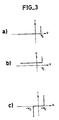
- - les figures 3a, b et c, des caractéristiques 1 = f(V) et C = f(V) des diodes utilisées ;
- - les figures 7, 8a à 8c, et 9 : des schémas concernant un mode de réalisation technologique d'un élément photosensible selon le mode de réalisation de la figure 5 ;
- - les figures 10, 11 a à j et 12a à h, un mode de réalisation du
circuit d'adressage 2 des figures 1, 4 et 5, et deux chronogrammes ; - - les figures 13, 14 et 15, deux modes de réalisation particuliers du circuit de lecture et de multiplexage et le chronogramme de la figure 14.
- - Figures 1, 4 and 5, a diagram of an embodiment of the device according to the invention;
- - Figures 2a to 2f and 6a to 6f, a timing diagram of the device of Figures 1 and 5;
- - Figures 3a, b and c,
characteristics 1 = f (V) and C = f (V) of the diodes used; - - Figures 7, 8a to 8c, and 9: diagrams concerning a technological embodiment of a photosensitive element according to the embodiment of Figure 5;
- - Figures 10, 11 a to j and 12a to h, an embodiment of the addressing
circuit 2 of Figures 1, 4 and 5, and two timing diagrams; - FIGS. 13, 14 and 15, two particular embodiments of the reading and multiplexing circuit and the timing diagram of FIG. 14.
Sur les différentes figures, les mêmes repères désignent les mêmes éléments, mais, pour des raisons de clarté, les cotes et proportions des divers éléments ne sont pas respectées.In the various figures, the same references designate the same elements, but, for reasons of clarity, the dimensions and proportions of the various elements are not observed.
La figure 1 représente le schéma d'un mode de réalisation du dispositif photosensible selon l'invention.FIG. 1 represents the diagram of an embodiment of the photosensitive device according to the invention.
Ce dispositif comporte une matrice photosensible 1 comportant un réseau de connexions horizontales ou lignes et un réseau de connexions verticales ou colonnes.This device comprises a
Sur la figure 1, on n'a représenté pour expliquer le fonctionnement du dispositif qu'une matrice 2x2, avec deux lignes Lp et Lp+1 et deux colonnes Ci et C2.In FIG. 1, only a 2x2 matrix has been shown to explain the operation of the device, with two rows Lp and Lp +1 and two columns Ci and C 2 .
Les lignes et les colonnes se croisent, sans être bien entendu en contact, et un élément photosensible relie chaque ligne et chaque colonne qui se croisent.The lines and the columns cross, without being of course in contact, and a photosensitive element connects each line and each column which cross.
Selon l'invention, chaque élément photosensible est constitué par la mise en série d'une capacité G, d'une photodiode D, en silicium amorphe par exemple, et d'un interrupteur électronique I.According to the invention, each photosensitive element consists of the series connection of a capacitor G, of a photodiode D, made of amorphous silicon for example, and of an electronic switch I.
Dans le mode de réalisation de la figure 1, on trouve en allant d'une ligne vers une colonne, la capacité G, puis la photodiode D dont l'anode est reliée à la capacité G en un point A et dont la cathode est reliée en un point B à l'interrupteur 1 connecté à une colonne.In the embodiment of FIG. 1, we find, going from a line to a column, the capacitance G, then the photodiode D whose anode is connected to the capacitance G at a point A and whose cathode is connected at point B at
L'invention s'applique quelle que soit la position respective des composants faisant partie de l'élément photosensible. On peut aussi inverser la position de l'anode et de la cathode de la photodiode D, c'est-à-dire par exemple dans le mode de réalisation de la figure 1, relier sa cathode au point A et son anode au point B. Cela entraîne des modifications des signaux de commande, des tensions aux points A et B et des charges qui circulent par rapport au mode de réalisation de la figure 1 qui va être décrit de façon détaillée ci-après. Ces modifications sont facilement accessibles à l'homme du métier.The invention applies regardless of the respective position of the components forming part of the photosensitive element. We can also reverse the position of the anode and the cathode of photodiode D, that is to say for example in the embodiment of FIG. 1, connect its cathode at point A and its anode at point B This leads to modifications of the control signals, of the voltages at points A and B and of the charges which circulate with respect to the embodiment of FIG. 1 which will be described in detail below. These modifications are easily accessible to those skilled in the art.
Le dispositif de la figure 1 comporte également un circuit d'adressage 2 dont les sorties sont reliées aux lignes de la matrice et un circuit de lecture et de multiplexage 3 dont les entrées sont reliées aux colonnes de la matrice.The device of FIG. 1 also includes an addressing
On a représenté sur la figure 1 un mode de réalisation du circuit de lecture et de multiplexage 3 dans lequel chaque colonne de la matrice est reliée à l'entrée négative d'un amplificateur opérationnel 4 dont l'entrée positive est à une tension constante qui peut être la masse du dispositif. Ces amplificateurs sont montés en intégrateurs et comportent une capacité C' connectée entre leur entrée négative et leur sortie. Un interrupteur i est monté en parallèle sur chaque capacité C' pour assurer sa remise à zéro. Les sorties des amplificateurs sont reliées à un multiplexeur 5, du type réseau d'interrupteurs ou CCD par exemple, dont la sortie fournit le signal de sortie S du dispositif.FIG. 1 shows an embodiment of the reading and multiplexing
On sait que les amplificateurs opérationnels montés en intégrateurs recopient sur leur entrée négative la polarisation de leur entrée positive. Dans le cas de la figure 1, l'entrée positive des amplificateurs est à une tension constante, par exemple à la masse du dispositif. Ces amplificateurs relient donc à la masse les colonnes qui sont reliées à leur entrée négative. On va décrire en se référant au chronogramme de la figure 2 le fonctionnement du disposiif de la figure 1 et plus particulièrement le fonctionnement d'un élément photosensible du dispositif de la figure 1, par exemple l'élément situé à l'intersection de la colonne Ci et de la pième ligne Lp de la matrice.We know that the operational amplifiers mounted as integrators copy the polarization of their positive input on their negative input. In the case of FIG. 1, the positive input of the amplifiers is at a constant voltage, for example at the ground of the device. These amplifiers therefore connect the columns which are connected to their negative input to ground. We will describe with reference to the timing diagram of Figure 2 the operation of the device of Figure 1 and more particularly the operation of a photosensitive element of the device of Figure 1, for example the element located at the intersection of the column Ci and the p th line Lp of the matrix.
Dans ce qui suit, on compte positivement les courants et les charges circulant depuis chaque élément photosensible vers l'amplificateur intégrateur situé en bas des colonnes.In what follows, the currents and charges flowing from each photosensitive element to the integrating amplifier located at the bottom of the columns are positively counted.
Sur la figure 2a, on a représenté les instants t1 à t12 considérés pour décrire le fonctionnement du dispositif de la figure 1 ainsi que les intervalles de temps 01 à ⌀12 considérés.
- La figure 2b représente des impulsions de tension Vpi et Vp2 circulant sur les lignes de la matrice.
- Les figures 2c et 2d représentent les tensions VA et VB aux points A et B de l'élément photosensible considéré.
- La figure 2e représente les quantités de charge circulant dans l'élément photosensible considéré.
- FIG. 2b represents voltage pulses Vpi and Vp 2 circulating on the lines of the matrix.
- Figures 2c and 2d show the voltages VA and V B at points A and B of the photosensitive element considered.
- FIG. 2e represents the quantities of charge circulating in the photosensitive element considered.
Sur le figure 2f, on a représenté, de façon symbolique la position ouverte ou fermée de l'interrupteur I appartenant à l'élément photosensible considéré.In Figure 2f, there is shown, symbolically the open or closed position of the switch I belonging to the photosensitive element considered.
On va examiner le fonctionnement du dispositif pendant les différentes phases 01 à ⌀12.We will examine the operation of the device during the different phases 0 1 to ⌀ 12 .
On applique une impulsion de tension VP1 sur l'ensemble des lignes de la matrice par l'intermédiaire du circuit d'adressage.A voltage pulse V P1 is applied to all of the rows of the matrix via the addressing circuit.
A l'instant ti, l'amplitude du signal Vp, passe de 0 à Vplet à l'instant t2, l'amplitude du signal Vp passe de VP1 à O.At time ti, the amplitude of signal Vp goes from 0 to Vp l and at time t 2 , the amplitude of signal Vp goes from V P1 to O.
La tension au point A suit, après charge de la capacité G la variation de tension intervenant sur les lignes, c'est-à-dire qu'à partir de l'instant ti, VA augmente puis se stabilise à la valeur Vc qui est la tension de coude ou de seuil de la photodiode D, ce qui polarise en direct la diode D dont la cathode est reliée à la masse par l'interrupteur 1 qui est passant.The voltage at point A follows, after charging the capacity G, the voltage variation occurring on the lines, that is to say that from the instant ti, VA increases then stabilizes at the value V c which is the elbow or threshold voltage of the photodiode D, which directly polarizes the diode D, the cathode of which is connected to ground by the
Pour simplifier l'explication du fonctionnement, on supposera que la diode D a une caractéristique C = f (V) telle que celle représentée sur la figure 3b. On peut cependant utiliser n'importe quel type de photodiode D, par exemple une photodiode du type PIN, PN ou Schottky.To simplify the explanation of operation, it will be assumed that the diode D has a characteristic C = f (V) such as that shown in FIG. 3b. However, any type of photodiode D can be used, for example a PIN, PN or Schottky type photodiode.
Pendant la phase 1, l'interrupteur I est fermé comme cela est représenté sur la figure 2f. On supposera pour simplifier qu'il s'agit d'un interrupteur parfait ce qui explique que la tension VB soit nulle.During
L'arrivée de l'impulsion VP1 provoque la circulation d'un courant correspondant à une charge Qi - figure 2e.The arrival of the pulse V P1 causes the circulation of a current corresponding to a charge Qi - Figure 2e.
A l'instant t2, VP1 revient à zéro et la tension VA devient négative et égale à
On choisit généralement CG supérieure à CD pour que la polarisation du point A soit proche de -Vpi. On peut choisir par exemple CG = 10 CD.We generally choose C G greater than C D so that the polarization of point A is close to -Vpi. One can choose for example C G = 10 C D.
La photodiode D de l'élément photosensible considéré se trouve polarisée en inverse car sa cathode est toujours reliée à la masse (VB = O) par l'interrupteur 1 toujours conducteur. La photodiode fonctionne alors dans le mode vidicon et va pouvoir détecter la lumière. Elle génère à partir de l'instant t2 un courant d'obscurité IOBS1 dont une fraction égale à
A l'instant t2, il a circulation d'une quantité de charge Q2 de signe contraire à celui de Qi.At the instant t 2 , it has circulation of a quantity of charge Q 2 of sign opposite to that of Qi.
Pendant cette phase, le dispositif reçoit le signal lumineux à analyser h s. On a représenté de façon symbolique sur la figure 2a l'application de ce flash lumineux. Ce flash crée un photocourant dans la photodiode D qui va avoir tendance à revenir à tension nulle. La tension VA augmente légèrement à partir de ts. On appelle Qs la quantité de charge crée et séparée dans la photodiode D. La fraction
C'est une phase d'attente qui sépare le flash lumineux de la lecture du dispositif. Elle peut éventuellement être supprimée. La tension VA est stable pendant cette phase. La tension VB est toujours nulle car l'interrupteur I est fermé.It is a waiting phase which separates the light flash from reading the device. It can possibly be deleted. The voltage VA is stable during this phase. The voltage V B is always zero because the switch I is closed.
Il y a circulation d'une quantité de charge Q4.There is circulation of a quantity of charge Q 4 .
Pendant les phases 02 à 04, la fraction égale à
A l'instant t5, on ouvre tous les interrupteurs. La photodiode D génère un courant d'obscurité IOBS2 qui n'est plus injecté dans la colonne mais qui s'accumule au point B. Le potentiel du point B se met à décroître avec une pente égale à IOBS2/CD. La charge maximale qu'il peut stocker égale 2Vc.CD. Le potentiel du point A en première approximation reste constant.At time t 5 , all the switches are opened. Photodiode D generates a dark current I OBS2 which is no longer injected into the column but which accumulates at point B. The potential of point B begins to decrease with a slope equal to I OBS2 / C D. The maximum charge it can store is 2Vc.CD. The potential of point A as a first approximation remains constant.
Pendant cette phase 0s, et si l'on suppose comme c'est généralement le cas qu'on lit la matrice photosensible de la première ligne L1 à la dernière Ln, on lit une à une les (p-1) premières lignes de la matrice grâce à des signaux délivrés sur ces lignes par le circuit d'adressage, de la même façon qu'on lit la pième ligne pendant les phases 6, 7, 8.During this phase 0s, and if we assume as is generally the case that we read the photosensitive matrix from the first line L 1 to the last Ln, we read one by one the first (p-1) lines of the matrix by means of signals delivered on these lines by the addressing circuit, in the same way as the p th line is read during
On constate que la lecture des (p-1) premières lignes n'est pas perturbée par la pième ligne puisque pendant la phase 05 les interrupteurs de la ligne Lp sont ouverts.It can be seen that the reading of the (p-1) first lines is not disturbed by the p th line since during phase 0 5 the switches of the line Lp are open.
Cette phase 06 marque le début de la lecture de la ligne Lp.This phase 0 6 marks the beginning of the reading of the line Lp.
A l'instant t6, on ferme les interrupteurs de la ligne Lp. Le point B est à nouveau relié à la masse et injecte alors dans la colonne une quantité des charges Q6 correspondant à la fraction
On applique sur la pième ligne et sur elle seule une impulsion de tension Vp2 d'amplitude supérieure à celle de VP1.A voltage pulse Vp 2 of amplitude greater than that of V P1 is applied to the p th line and to it alone.
Le potentiel du point A augmente et se stabilise à Vc lorsque la photodiode D conduit. Du fait de la mise en direct de la photodiode D, il y a circulation d'une quantité de charge Q7 de signe contraire à celui des charges Q2, Q3, Q4, Q6 et de même signe que Qi et Qs. La quantité de charge Q7 contient l'information signal au même titre que Q3. Il faut remarquer que Q3 n'est pas exploitable car le flash lumineux est envoyé simultanément à tout le dispositif et toutes les photodiodes débitent simultanément sur les colonnes qui fournissent la valeur moyenne du signal lumineux appliqué.The potential of point A increases and stabilizes at V c when photodiode D conducts. Due to the directing of photodiode D, there is circulation of a quantity of charge Q 7 of sign opposite to that of charges Q 2 , Q 3 , Q 4 , Q 6 and of the same sign as Qi and Qs . The charge quantity Q7 contains the signal information in the same way as Q 3 . It should be noted that Q 3 cannot be used because the light flash is sent simultaneously to the entire device and all the photodiodes flow simultaneously on the columns which provide the average value of the light signal applied.
Selon l'invention, on va obtenir l'information signal à partir de la charge Q7.According to the invention, the signal information will be obtained from the load Q 7 .
Le dispositif selon l'invention comporte des éléments photosensibles ayant chacun une capacité, une photodiode et un interrupteur. Il n'y a donc pas de courant continu qui circule à travers les éléments photosensibles.The device according to the invention comprises photosensitive elements each having a capacity, a photodiode and a switch. There is therefore no direct current flowing through the photosensitive elements.
En conséquence, si l'on suppose que les impulsions VP1 et VP2 sont identiques, on peut écrire : ΣQi = O, avec i = 2 à 7. Du fait de la différence d'amplitude entre les impulsions VP1 et VP2, il faut écrire : Qi = CG (Vp2 - VP1) avec i = 2 à 7, ce qui donne :
- Q7=-(Q2+Q3+Q4+Q5+Q6)+CG(VP2-VP1).
- Q 7 = - (Q 2 + Q 3 + Q 4 + Q 5 + Q 6 ) + C G (V P2 -V P1 ).
L'intégration sur les amplificateurs reliés aux colonnes des charges Q7 provenant des photodiodes de la ligne Lp permet donc d'obtenir l'information signal pour cette ligne.Integration on the amplifiers connected to the columns of the charges Q 7 coming from the photodiodes of the line Lp therefore makes it possible to obtain the signal information for this line.
Selon l'invention, on compense la fraction du courant d'obscurité IOBS2 égale à
Pour réaliser cette compensation, on somme dans les amplificateurs intégrateurs les charges Q6 et Q7.
- Q6 + Q7 = - (Q2 + Q3 + Q4 + Q5) + CG (VP2 - VP1)
- Q 6 + Q 7 = - (Q 2 + Q 3 + Q 4 + Q 5 ) + C G (V P2 - V P1 )
On a donc éliminé la quantité de charges Q6 provenant du courant d'obscurité IOBS2.We therefore eliminated the quantity of charges Q 6 coming from the dark current I OBS2 .
En conséquence, en sommant les charges qui circulent entre l'instant te où l'on ferme les interrupteurs de la ligne Lp et l'instant t7 où l'impulsion de lecture Vp2 est appliquée à la ligne Lp, on arrive à lire les éléments photosensible de la ligne Lp et à compenser Q6 stockée par la ligne Lp alors qu'on lit les autres lignes - phase 05.Consequently, by summing the charges which circulate between the instant te when the switches of the line Lp are closed and the instant t 7 where the reading pulse Vp 2 is applied to the line Lp, we can read the photosensitive elements of the line Lp and to compensate Q 6 stored by the line Lp while the other lines are read - phase 0 5 .
Le courant d'obscurité délivré pendant la phase 05 n'intervient plus ni pour sa valeur moyenne ni pour son bruit.The dark current delivered during phase 0 5 no longer intervenes either for its average value or for its noise.
On fait se déverser ce courant au temps t7 et on le compense en réalisant la somme Q6 + Q7.This current is poured out at time t 7 and is compensated for by making the sum Q 6 + Q 7 .
Pour réaliser la somme Q6 + Q7, le circuit de lecture et de multiplexage assure la lecture de chaque photodiode de la ligne sélectionnée en sommant les charges qui circulent en commençant avant que les interrupteurs de la ligne sélectionnée soient fermés et en terminant alors que l'impulsion Vp2 est appliquée à la ligne sélectionnée.To achieve the sum Q 6 + Q 7 , the reading and multiplexing circuit reads each photodiode of the selected line by summing the charges which circulate, starting before the switches of the selected line are closed and ending while the pulse Vp 2 is applied to the selected line.
En ce qui concerne le courant d'obscurité IOBS1 dont il a été question pendant la phase 4, la somme Q6 + Q7 montre qu'il n'intervient que pendant la phase 3 correspondant à l'éclairement signal et pendant les phases de sécurité 2 et 4 dont la durée peut être faible devant celle de la phase 5.Regarding the dark current I OBS1 discussed during
L'utilisation d'une impulsion de lecture Vp2 d'amplitude supérieure à l'impulsion de précharge VP1 crée la circulation d'une charge supplémentaire CG (VP2 - VP1) pendant la phase 7 qui accélère le transfert de Q7 sur la colonne. Sans cette charge supplémentaire, le transfert est lent.The use of a reading pulse Vp 2 of amplitude greater than the precharge pulse V P1 creates the circulation of an additional charge C G (V P2 - V P1 ) during
En effet, lors de l'arrivée de l'impulsion VP2, le point de polarisation de la photodiode D se trouve déplacé en direct, le déplacement instantané valant
L'utilisation d'une impulsion VP2 d'amplitude supérieure à VP1 déplace la valeur moyenne du point de polarisation de la photodiode en direct dans une zone où sa résistance dynamique est plus faible, et donc accélère le phénomène de retour vers la valeur d'équilibre.The use of a pulse V P2 of amplitude greater than V P1 displaces the average value of the point of polarization of the photodiode in direct in a zone where its dynamic resistance is weaker, and thus accelerates the phenomenon of return towards the value of balance.
La phase 6 peut être supprimée. La quantité de charge qui circule lorsque la tension de ligne passe à VP2 vaut alors Qs + Q7. La fermeture des interrupteurs se fait simultanément avec le passage à VP2.
A l'intant ta, VP2 revient à zéro. Il se produit une variation de VA analogue à celle qui a lieu à l'instant t2. Le potentiel des points A de la ligne Lp passe à
Comme les interrupteurs I sont toujours fermés, les photodiodes D des éléments photosensibles de la ligne Lp se retrouvent polarisées en inverse.As the switches I are always closed, the photodiodes D of the photosensitive elements of the line Lp are found to be reverse biased.
Il y a circulation d'une quantité de charges Q8.There is circulation of a quantity of charges Q 8 .
Pour lire les charges signal, on peut sommer les charges Q6 + Q7 + Q8. Par rapport à la somme Q6 + Q7, l'intérêt est que le terme constant, indépendant des charges-signal et de IOBS2 est plus faible.To read the signal charges, we can add the charges Q 6 + Q 7 + Q 8 . Compared to the sum Q 6 + Q 7 , the advantage is that the constant term, independent of the signal charges and of I OBS2 is weaker.
Il faut alors que le circuit de lecture et de multiplexage assure la lecture de chaque photodiode de la ligne sélectionnée en sommant les charges qui circulent en commençant avant que les interrupteurs de la ligne sélectionnée soient fermés, en poursuivant alors que l'impulsion VP2 est appliquée à la ligne sélectionnée, et en terminant alors que l'impulsion VP2 est revenue à zéro.It is then necessary that the reading and multiplexing circuit ensures the reading of each photodiode of the selected line by summing the charges which circulate starting before the switches of the selected line are closed, continuing while the pulse V P2 is applied to the selected line, and ending while the V P2 pulse has returned to zero.
A l'instant t9 on ouvre les interrupteurs de la ligne Lp qui vient d'être lue. On lit alors les lignes LP+1 à Ln et leur lecture n'est pas perturbée par le courant d'obscurité des photodiodes de la ligne Lp dont les interrupteurs sont ouverts.At time t 9 the switches of the line Lp which has just been read are opened. The lines L P + 1 to L n are then read and their reading is not disturbed by the dark current of the photodiodes of the line Lp whose switches are open.
L'ouverture de ces interrupteurs provoque la circulation d'une quantité de charge Q9 dans le cas où les interrupteurs I ne sont pas parfaits. Comme au début de la phase 5, la tension VA reste constante, en première approximation, alors que la tension VB décroît. Pour lire les charges-signal, on peut réaliser la somme :
- Q6 + Q7 + Q8 + Qs.
- Q 6 + Q 7 + Q 8 + Qs.
Il faut alors sommer les charges circulant avant que les interrupteurs de la ligne sélectionnée soient fermés et jusqu'à leur ouverture.The loads circulating must then be summed before the switches of the selected line are closed and until they open.
La lecture de la Pième ligne se fait en ouvrant l'interrupteur i sur la contre-réaction des amplificateurs intégrateurs juste avant la phase 6. On commence alors la sommation des charges. On peut lire les charges grâce au muliplexeur, lorsque les amplificateurs intégrateurs ont sommé les charges Q6 + Q7 ou bien Q6 + Q7 + Q8 ou bien Q6 + Q7 + Q8 + Q9. Ensuite, on referme les interrupteurs i, de façon à remettre les capacités des intégrateurs à zéro avant l'arrivée des charges provenant de la ligne p+1.The P th line is read by opening the switch i on the feedback of the integrating amplifiers just before
A la fin de la phase 9, la lecture de toutes les lignes du dispositif est terminée. Avant de commencer le cycle d'imagerie suivant, on veut retrouver une même configuration de potentiels, c'est-à-dire qu'il faut pouvoir écrire pour le cycle d'imagerie qui se termine l'équation suivante :
- Σ Q; = O, ce qui s'écrit aussi, puisque ΣQi = CG(Vp2 - Vpi), avec i = 2 à 7 :
- Q8 + Q9 + Q10 + Q11 + Q12 = - Q1 - CG(VP2 - VP1), où Q10, Q11 et Q12, sont les charges générées au cours des dernières phases 10, 11 et 12 du cycle d'imagerie.
- Σ Q; = O, which is also written, since ΣQ i = C G (Vp 2 - Vpi), with i = 2 to 7:
- Q 8 + Q 9 + Q 10 + Q 11 + Q 12 = - Q 1 - C G (V P2 - V P1 ), where Q 10 , Q 11 and Q 12 , are the charges generated during the
last phases
La charge Qi étant positive, il faut pour que l'équation ci-dessus soit vérifiée que la condition suivante soit vérifiée : Q8 + Q9 + Q10 + Q11 + Q12|≧|CG. (VP2 - VP1).|The charge Qi being positive, it is necessary for the above equation to be verified that the following condition is satisfied: Q 8 + Q 9 + Q 10 + Q 11 + Q 12 | ≧ | C G. (V P2 - V P1 ).
On va donc au cours des phases 10, 11 et 12, et en particulier au cours de la phase 11 générer des charges telles que l'inégalité précédente soit vérifié.We will therefore during
A l'instant tio, on ferme tous les interrupteurs I du dispositif. Il y a circulation d'une quantité de charge Q10 égale àAt time tio, all the switches I of the device are closed. There is circulation of a quantity of charge Q 10 equal to

Pendant cette phase, on éclaire les photodiodes pour les faire fuir et provoquer la circulation d'une quantité de charge Q11 suffisante pour que l'inégalité suivante soit vérifiée :
- |Q8 + Q9 + Q10 + Q11 + Q12|≧|CG. (VP2 - VP1)|.
- | Q8 + Q 9 + Q 10 + Q 11 + Q 12 | ≧ | C G. (V P2 - V P1 ) |.
On éclaire généralement simultanément tout le dispositif, on est donc amené à choisir une valeur moyenne pour Qa et pour Q9.The entire device is generally illuminated simultaneously, so we have to choose an average value for Qa and for Q 9 .
On peut aussi ne pas tenir compte de Q8 et Q9 et ne s'attacher à satisfaire que la relation suivante :
- 1 Q10 + Q11 + Q12|≧|CG(VP2VP1)|, c'est-à-dire qu'il faut que la valeur absolue de la somme des charges ayant circulé après la lecture de toutes les lignes soit supérieur ou égale à ICG.(VP2 - VP1)|
- 1 Q 10 + Q 11 + Q 12 | ≧ | C G (V P2 V P1 ) |, that is to say that the absolute value of the sum of the charges having circulated after reading all the lines be greater than or equal to IC G. (V P2 - V P1 ) |
On appelle la phase 11 la phase de remise à zéro des photodiodes.
Dans le cas de la détection de rayons X, si le scintillateur placé devant le dispositif est opaque, on peut éclairer la face arrière du panneau. Il faut alors que le substrat sur lequel est réalisé le dispositif photosensible soit transparent. On peut utiliser un substrat en verre ou en quartz par exemple.In the case of X-ray detection, if the scintillator placed in front of the device is opaque, the rear face of the panel can be lit. The substrate on which the photosensitive device is made must therefore be transparent. One can use a glass or quartz substrate for example.
La quantité de charges Q11 peut aussi être produite en appliquant aux lignes une impulsion de tension qui pousse les photodiodes D en inverse au-dela de leur tension de claquage, tout en restant dans les limites du claquage réversible, de façon à provoquer la circulation d'une quantité de charges Q11 suffisante pour satisfaire l'inégalité citée plus haut dans le cas d'une remise à zéro par voie optique.The quantity of charges Q 11 can also be produced by applying a voltage pulse to the lines which pushes the photodiodes D in reverse beyond their breakdown voltage, while remaining within the limits of reversible breakdown, so as to cause circulation. of a quantity of charges Q 11 sufficient to satisfy the inequality cited above in the case of a reset by optical means.
La phase 12 est une phase qui sépare un cycle d'imagerie du cycle suivant. Il y a circulation d'une quantité de charge Qi2.
Une nouvelle phase 1 commence ensuite avec l'application d'une impulsion de tension VP1 à toutes les lignes du dispositif. La charge Q1 qui circule évacue l'excédent de charges qui a pu être apporté lors de la phase 11. Il n'est donc pas nécessaire de calibrer précisément cette charge Q11. On retrouve la même configuration électrique que lors de la phase 1 de l'image précédente.A
Dans le mode de réalisation de l'invention qui vient d'être exposé, tous les interrupteurs sont fermés entre l'instant tio correspondant à la fin de la lecture du dispositif et l'instant t4 du cycle d'imagerie suivant qui marque le début d'une nouvelle lecture du dispositif.In the embodiment of the invention which has just been exposed, all the switches are closed between the instant tio corresponding to the end of the reading of the device and the instant t 4 of the following imaging cycle which marks the start of a new reading of the device.
Il faut signaler que lorsqu'on applique le flash lumineux correspondant au signal à lire, il est possible de laisser les interrupteurs ouverts. Le courant s'accumule au point B. Il faut alors fermer les interrupteurs avant que ne commence la lecture du dispositif pour autoriser les charges-signal à se déverser sur les lignes et les colonnes.It should be noted that when the light flash corresponding to the signal to be read is applied, the switches can be left open. Current accumulates at point B. It is then necessary to close the switches before reading of the device begins to authorize the signal charges to be discharged on the rows and the columns.
En conséquence, les interrupteurs du dispositif doivent être fermés pendant les phases 01 et 04 alors que pendant les phases 02 et 03, ils peuvent être indifféremment ouverts ou fermés.Consequently, the switches of the device must be closed during phases 0 1 and 0 4, while during phases 0 2 and 0 3 , they can be either open or closed.
De même, les interrupteurs du dispositif peuvent être indifféremment fermés ou ouverts pendant les phases ⌀10 à ⌀12.Likewise, the switches of the device can be closed or open either during phases les 10 to ⌀ 12 .
La solution préférée consiste à laisser les interrupteurs fermés pendant les phases 10, 11 et 12, et même de la phase 10 à la fin de la phase 4 du cycle d'imagerie suivant.The preferred solution is to leave the switches closed during
On peut utiliser divers modes de réalisation des interrupteurs I en série dans chaque élément photosensible.Various embodiments of the switches I can be used in series in each photosensitive element.
La figure 4 représente un mode de réalisation où chaque interrupteur I est constitué par un transistor T. On peut utiliser par exemple un TFT en silicium amorphe, un MOSFET ou un JFET.FIG. 4 represents an embodiment where each switch I is constituted by a transistor T. One can use for example a TFT in amorphous silicon, a MOSFET or a JFET.
La commande de l'ouverture ou de la fermeture des interrupteurs est alors assurée par un réseau supplémentaire de connexions horizontales L'p et L'P+1 qui sont reliées à des sorties supplémentaires du circuit d'adressage.The control of the opening or closing of the switches is then ensured by an additional network of horizontal connections L'p and L ' P + 1 which are connected to additional outputs of the addressing circuit.
Dans le mode de réalisation de la figure 5, chaque interrupteur est constitué de deux diodes montées tête-bêche, di et d2.In the embodiment of FIG. 5, each switch consists of two diodes mounted head to tail, di and d 2 .
Pour pouvoir bien commander ces interrupteurs, il faut que la capacité CD de la photodiode soit très supérieure à la somme des capacités Cdi et Cd2 des deux diodes. Ainsi, on considère pour simplifier dans l'explication de fonctionnement du dispositif que lorsqu'une tension est appliquée aux bornes de chaque élément photosensible, elle se retrouve aux bornes de l'interrupteur.To be able to properly control these switches, the capacitance C D of the photodiode must be much greater than the sum of the capacitances C d i and C d2 of the two diodes. Thus, it is considered for simplicity in the explanation of operation of the device that when a voltage is applied to the terminals of each photosensitive element, it is found at the terminals of the switch.
A titre d'exemple on peut choisir : Co = 50.(Cdi + Cd2).As an example we can choose: Co = 50. (C d i + C d2 ).
De même pour que l'interrupteur ainsi réalisé soit satisfaisant il faut que les diodes di et d2 suivent la caractéristique 1 = f (V) de la figure 3 a où le courant est nul pour une tension inférieure à la tension de seuil Vc. Cette hypothèse est justifiée car les diodes d1 et d2 ayant des capacités de faibles valeurs ont généralement de faibles surfaces et un courant de fuite faible. Sur cette caractéristique, les diodes ont aussi une impédance dynamique nulle pour une tension supérieure à Vc.Similarly, for the switch thus produced to be satisfactory, the diodes di and d 2 must follow the characteristic 1 = f (V) of FIG. 3 a where the current is zero for a voltage lower than the threshold voltage Vc. This hypothesis is justified because the diodes d 1 and d 2 having capacitances of low values generally have small surfaces and a low leakage current. On this characteristic, the diodes also have a zero dynamic impedance for a voltage greater than Vc.
L'association de deux diodes di et d2 ayant la caractéristique I = f (V) de la figure 3a donne un interrupteur ayant la caractéristique I = f (V) de la figure 3c.The association of two diodes d i and d 2 having the characteristic I = f (V) of FIG. 3a gives a switch having the characteristic I = f (V) of FIG. 3c.
Entre les tensions - Vc et + Vc, l'interrupteur est fermé, alors qu'il est ouvert pour des tensions supérieures à + Vc et inférieures à - Vc.Between the voltages - Vc and + Vc, the switch is closed, while it is open for voltages higher than + Vc and lower than - Vc.
Lorsqu'on utilise dans le dispositif selon l'invention, un interrupteur constitué de de deux diodes d1 et d2 montées tête-bêche, on commande cet interrupteur en modulant le potentiel des lignes de 2Vc.When a switch consisting of two diodes d 1 and d 2 mounted head to tail is used in the device according to the invention, this switch is controlled by modulating the potential of the lines of 2Vc.
Pour simplifier l'explication du fonctionnement on considère de plus que les diodes di et d2, ont une capacité constante en fonction de la tension V, lorsque celle-ci est inférieur à Vc, comme cela est représenté sur la figure 3b.To simplify the explanation of operation, it is further considered that the diodes di and d 2 have a constant capacity as a function of the voltage V, when the latter is less than Vc, as shown in FIG. 3b.
Cette hypothèse est vérifiée en particulier si les diodes d1 et d2 sont des diodes PIN.This hypothesis is verified in particular if the diodes d 1 and d 2 are PIN diodes.
La figure 6 représente le chronogramme du dispositif de la figure 5 dont le fonctionnement est peu différent de celui de la figure 1.FIG. 6 represents the timing diagram of the device of FIG. 5, the operation of which is little different from that of FIG. 1.
Dans ce qui suit, on ne va pas reprendre l'explication détaillée du dispositif de la figure 5. En ce qui concerne les figures 5 et 6, on se contentera de souligner les différences par rapport aux figures 1 et 2, ces différences tenant essentiellement au fait que les interrupteurs 1 constitués de deux diodes d1 et d2 montées tête-bêche ne sont pas des interrupteurs parfaits.In what follows, we will not repeat the detailed explanation of the device in FIG. 5. With regard to FIGS. 5 and 6, we will simply highlight the differences compared to FIGS. 1 and 2, these differences essentially being to the fact that the
La diode d1 et la photodiode D se trouvent polarisées en direct par la tension VP1. En conséquence, pendant l'application de la tension VP1, la tension VA se fixe à 2Vc et la tension VB à Vc, si l'on admet que Vc est la tension de seuil des diodes D, di et d2.Diode d 1 and photodiode D are forward biased by voltage V P1 . Consequently, during the application of the voltage V P1 , the voltage VA is fixed at 2Vc and the voltage V B at Vc, if it is assumed that Vc is the threshold voltage of the diodes D, di and d 2 .
Lorsque l'impulsion VP1 revient à zéro, la variation de tension est d'abord absorbée par les diodes di et d2 alors que la tension VB passe de + Vc à - Vc. En fait la fraction de la variation de tension absorbée par les diodes di et d2 et par le point A est la suivante :
Ensuite le point A varie de
On ne tiendra pas compte du courant d'obscurité des diodes d1 et d2 qui sont de faibles valeurs par rapport à ceux des photodiodes D.The dark current of diodes d 1 and d 2, which are small compared to those of photodiodes D, will not be taken into account.
Pas de changement.No change.
Pour provoquer l'ouverture des interrupteurs, on envoie sur les lignes une tension égale à 2Vc. La tension VA reste sensiblement constante mais subit une augmentation de 2Vc à l'instant ts. De même, la tension VB passe à + Vc à l'instant t5 pour décroître ensuite, avec une pente égale à IOBS2/CD.To cause the opening of the switches, a voltage equal to 2Vc is sent to the lines. The voltage VA remains substantially constant but undergoes an increase of 2Vc at time ts. Similarly, the voltage V B goes to + Vc at time t 5 to then decrease, with a slope equal to I OBS2 / CD .
On ferme les interrupteurs de la ligne Lp en ramenant à zéro le potentiel de cette ligne. Le potentiel VB se fixe à - Vc.The switches of the line Lp are closed by bringing the potential of this line to zero. The potential V B is fixed at - Vc.
La tension VA se stabilise à 2Vc et la tension VB à Vc.The voltage VA stabilizes at 2Vc and the voltage V B at Vc.
Le point B varie de 2Vc et passe à - Vc et le point A varie de
Le potentiel de la ligne Lp passe à 2Vc, pour provoquer l'ouverture des interrupteurs de cette ligne. A l'instant t9, les tensions VA et VB varient de + 2Vc. La tension VB passe à + Vc puis décroît avec une pente égale à IOBS2/CD.The potential of line Lp goes to 2Vc, to cause the opening of the switches of this line. At time t 9 , the voltages VA and V B vary from + 2Vc. The voltage V B goes to + Vc then decreases with a slope equal to I OBS2 / C D.
L'expression de la somme Q6 + Q7 + Qa + Qg montre que les capacités Cdi et Cd2 n'interviennent plus, ce qui est intéressant notamment pour éviter que des dispersions sur ces valeurs pour les différents éléments photosensibles n'entraînent des erreurs sur les signaux de lecture.The expression of the sum Q 6 + Q7 + Qa + Q g shows that the capacitances C d i and C d2 no longer intervene, which is interesting in particular to avoid dispersions on these values for the different photosensitive elements n ' cause errors on the read signals.
On ferme tous les interrupteurs en ramenant l'ensemble des lignes du dispositif à zéro. La tension VA diminue de 2Vc puis augmente pendant la phase 11. La tension VB se stabilise à - Vc.All the switches are closed by bringing all the lines of the device to zero. The voltage VA decreases by 2Vc then increases during
Le dispositif représenté sur la figure 5 présente l'avantage suivant. Lors de la lecture d'une ligne d'éléments photosensibles, les interrupteurs appartenant aux éléments photosensibles des autres lignes du dispositif sont ouverts. Toutes ces autres lignes ne sont en contact avec les colonnes que par l'intermédiaire de trois capacités en parallèle qui sont les capacités Cdi et Cd2 des diodes d1 et d2 à l'état bloqué et la capacité de croisement Cc des lignes et des colonnes. Ces capacités Cdi, Cd2 et Cc sont faibles. La ligne qui est lue est en contact avec les colonnes par la capacité CG appartenant à chaque élément photosensible. En conséquence, la capacité Ccol d'une colonne d'un dispositif de q ligne, qui est vue par le circuit de lecture et de multiplexage lorsqu'on lit une ligne vaut :
- Ccol = GG + (q-1) . (Cd1 + Cd2 + Cc)
- Ccol≃ (q-1).(Cd1 + Cd2 + Cc), lorsque Q est grand.
- C col = GG + (q-1). (C d1 + Cd 2 + Cc)
- C col ≃ (q-1). (C d1 + C d2 + Cc), when Q is large.
Cette capacité Ceci peut être modérée et permet la conception d'un circuit de lecture et de multiplexage relativement simple.This capacity This can be moderate and allows the design of a relatively simple reading and multiplexing circuit.
Enfin, un autre avantage de ce dispositif est qu'il ne nécessite que la réalisation de diodes et de capacités et qu'il est donc particulièrement simple à réaliser, comme on va le voir sur un exemple de réalisation technologique.Finally, another advantage of this device is that it only requires the production of diodes and capacitors and that it is therefore particularly simple to produce, as will be seen in an example of technological implementation.
De plus, ce dispositif ne nécessite pas, comme lorsque les interrupteurs sont constitués par des transistors, un réseau supplémentaire de lignes pour commander les transistors.In addition, this device does not require, as when the switches are constituted by transistors, an additional network of lines to control the transistors.
Les figures 7, 8a, b et c, et 9 concernent un mode de réalisation technologique du dispositif de la figure 5, et plus particulièrement d'un élément photosensible de ce dispositif.Figures 7, 8a, b and c, and 9 relate to a technological embodiment of the device of Figure 5, and more particularly of a photosensitive element of this device.
La figure 7 est une vue de dessus de l'élément photosensible ainsi réalisé, et les figures 8a à c sont des vues en coupe selon les plans AA', BB' et CC' de ce dispositif.Figure 7 is a top view of the photosensitive element thus produced, and Figures 8a to c are sectional views along the planes AA ', BB' and CC ' of this device.
On désigne par la référence 6 le substrat transparent sur lequel sont réalisés les éléments photosensibles.The transparent substrate on which the photosensitive elements are made is designated by the
Ce substrat porte un premier niveau conducteur 7 qui est utilisé pour réaliser les colonnes, le contact avec les colonnes de la diode di - figure 8a - et le contact au point B de la diode D avec les diodes di et d2- figures 8a et b.This substrate carries a first
Dans le cas où la remise à zéro optique est effectuée à travers le substrat, le premier niveau conducteur 7 doit être transparent.In the case where the optical reset is carried out through the substrate, the first
Sur ce premier niveau conducteur 7, on dépose et on grave une couche PIN de façon à réaliser les diodes di, d2 et D.On this first
Sur la figure 7, les diodes di et d2 et D sont délimitées par des pointillés.In FIG. 7, the diodes d i and d 2 and D are delimited by dotted lines.
On dépose une couche d'isolant 8 qui sert dans la partie où il recouvre la diode D à constituer la capacité G et qui sert aussi à isoler le passage du deuxième niveau conducteur 9. On ouvre les quatre contacts suivants : un contact sur di, figure 8a - un contact sur d2, figure 8b - un contact sur la colonne pour relier d2 - un contact sur le contact situé sous la diode D pour relier la diode di à la diode D.An insulating
On dépose la deuxième niveau conducteur 9 et on le grave pour relier la diode di au point B - figure 8a, pour relier la diode d2 à la colonne - figure 8b et pour réaliser les lignes.The second
Ce deuxième niveau conduteur 9 doit être transparent au rayonnement lumineux à analyser.This
Sur les figures 8a, b et c, on a représenté un scintillateur 10 qui fait face à l'élément photosensible.In Figures 8a, b and c, there is shown a
Sur le mode de réalisation de la figure 8c, on voit qu'on n'a pas réalisé exactement un élément photosensible tel que ceux représentés sur la figure 5, mais un élément photosensible tel que celui représenté sur la figure 9.In the embodiment of FIG. 8c, it can be seen that a photosensitive element such as those represented in FIG. 5 has not been produced exactly, but a photosensitive element such as that represented in FIG. 9.
Il y a en parallèle sur chaque élément photosensible constitué par la mise en série d'une capacité G, d'une diode D et de deux diodes di et d2 montées tête-bêche, une capacité G' en série avec une diode D'. La capacité de l'ensemble constitué par la capacité G' et la diode D' en série est inférieure ou égale à la capacité qu'aurait présenté un simple isolant. De plus, ainsi, la probabilité de défaut par court-circuit est plus faible du fait de la diode D' qui se trouve polarisée en inverse si la capacité G' est en court-circuit.There is in parallel on each photosensitive element constituted by the series connection of a capacitance G, of a diode D and of two diodes d i and d 2 mounted head to tail, a capacitance G 'in series with a diode D '. The capacity of the assembly constituted by the capacity G ′ and the diode D ′ in series is less than or equal to the capacity that a simple insulator would have presented. In addition, thus, the probability of fault by short-circuit is lower due to the diode D 'which is reverse biased if the capacitance G' is in short-circuit.
Il est bien sûr possible si on le souhaite de ne conserver que l'isolant au point de croisement des lignes et des colonnes en gravant le dépôt PIN.It is of course possible if you wish to keep only the insulation at the point of intersection of the rows and columns by engraving the PIN deposit.
On a vu que les interrupteurs 1 de la figure 1 pouvaient être constitués par un transistor ou par deux diodes montées tête-bêche.We have seen that the
Il est également possible de réaliser ces interrupteurs par une seule diode en utilisant aussi bien la partie de sa caractéristique où elle est passante que la partie où elle est en inverse et fournit de façon sensiblement reproductible un courant de fuite. Il faut donc utiliser une diode dont on maîtrise sensiblement la tension de claquage inverse et dont cette tension n'est pas trop élevée.It is also possible to make these switches with a single diode using both the part of its characteristic where it is conducting and the part where it is in reverse and provides a substantially reproducible leakage current. It is therefore necessary to use a diode whose reverse breakdown voltage is substantially mastered and whose voltage is not too high.
Les interrupteurs 1 peuvent également être constitués d'éléments multi-couches du type NIN ou PIP.The
La figure 10 représente un mode de réalisation du circuit d'adressage des lignes 2 qui est représenté sur les figures 1, 4 et 5.FIG. 10 represents an embodiment of the addressing circuit for
Ce circuit comporte un registre à décalage logique 11, piloté par au moins une horloge H. Dans l'exemple de la figure 10, ce registre comporte six sorties Ri à Rs. Des transistors h à Is sont commandés par les sorties Ri à Rs et reliés entre une tension V1 et une sortie du circuit d'adressage Si à Ss. Entre chaque sortie du circuit et une tension Vcom, on connecte une résistance de rappel Roi à Ro5 qui impose la tension Vcom sur les sorties du circuit reliées à des lignes qui ne sont pas lues.This circuit comprises a
La figure 11 est un chronogramme concernant le dispositif de la figure 10.FIG. 11 is a timing diagram relating to the device of FIG. 10.
La figure 11 a concerne l'éclairement signal. On a représenté de façon symbolique le signal lumineux à analyser hvs qui est appliqué entre les instants ts et t4.Figure 11a concerns signal illumination. The light signal to be analyzed hvs which is applied between the instants ts and t 4 has been represented symbolically.
De la même façon sur la figure 11 b, on a indiqué que l'éclairement de remise à zéro hvRAZ est appliqué entre les instants t11 et ti2.In the same way in FIG. 11 b, it has been indicated that the reset zero illumination hv RAZ is applied between the instants t 11 and ti 2 .
Sur la figure 11 c, on a représenté le signal Vcom. Cette tension Vcom est constituée par les différentes tensions à appliquer aux lignes lorsqu'on ne les lit pas.In FIG. 11 c, the signal V com is shown . This voltage V com is made up of the different voltages to be applied to the lines when they are not read.
On voit sur la figure 11c que la tension Vcom comporte une impulsion de tension Vpi de ti à t2, et une tension égale à 2Vc de t4 à ts. Pendant le reste du temps, la tension Vcom est à zéro, c'est à dire à la masse.It can be seen in FIG. 11c that the voltage V com comprises a voltage pulse Vpi from ti to t 2 , and a voltage equal to 2Vc from t 4 to ts. During the rest of the time, the voltage Vcom is at zero, that is to say to ground.
Sur la figure 11 d, on a représenté le signal d'horloge H du registre à décalage 11 de la figure 10.FIG. 11 d shows the clock signal H of the
Les figures 11e, f et g montrent que chaque impulsion d'horloge du signal H provoque le passage au niveau haut d'une sortie du registre. Sur ces figures, les sorties Ri, R2... puis ensuite la sortie Rs passent au niveau haut.FIGS. 11e, f and g show that each clock pulse of the signal H causes the output of the register to go high. In these figures, the outputs Ri, R 2 ... then then the output Rs go to the high level.
La figure 11 h montre le signal Vi. Ce signal Vi est constitué par les différentes tensions à appliquer à une ligne pour la lire. Ce signal Vi est au niveau O, et alors que l'une des sorties du registre Ri, R2...R5 passe au niveau haut, le signal Vi génère une impulsion de tension VP2.Figure 11h shows the signal Vi. This signal Vi is formed by the different voltages to be applied to a line to read it. This signal Vi is at level O, and while one of the outputs of the register Ri, R 2 ... R 5 goes high, the signal V i generates a voltage pulse V P2 .
Sur la figure 11 i, on a représenté les tensions sur la sortie Si qui commande la ligne Li du dispositif.In FIG. 11 i, the voltages are shown on the output Si which controls the line Li of the device.
Tant que le signal Ri n'est pas au niveau haut, le transistor I1 est bloqué et la résistance de rappel impose la tension Vcom sur la sortie Si. On voit sur la figure 11 i que tant que le signal Ri est au niveau bas, la tension Vcom est imposée sur la sortie Si. Lorsque le signal Ri est au niveau haut, la tension Vi se retrouve sur la sortie Si.As long as the signal Ri is not at the high level, the transistor I 1 is blocked and the restoring resistance imposes the voltage Vcom on the output Si. It can be seen in FIG. 11 i that as long as the signal Ri is at the low level , the voltage V c om is imposed on the output Si. When the signal Ri is at the high level, the voltage Vi is found on the output Si.
Pour accélérer le retour à Vcom des lignes lorsque leur lecture est terminée, on a disposé dans le mode de réalisation de la figure 10 un transistor Ji à J5 en parallèle sur les résistances de rappel. Les transistors Ji à Js sont du même type que les transistors I1 à Is mais ils sont commandés par la sortie suivante du registre.To accelerate the return to V com of the lines when their reading is finished, there has been arranged in the embodiment of FIG. 10 a transistor Ji to J 5 in parallel on the restoring resistors. The transistors J i to Js are of the same type as the transistors I 1 to I s but they are controlled by the following output of the register.
Ainsi le transistor Ji est commandé par la sortie R2, le transistor J2 est commandé par la sortie Ra...Thus the transistor Ji is controlled by the output R 2 , the transistor J 2 is controlled by the output Ra ...
Lorsque la sortie R1 est au niveau haut, la tension Vi se retrouve sur la sortie Si et le transistor J1 est bloqué.When the output R 1 is at the high level, the voltage V i is found on the output Si and the transistor J 1 is blocked.
Lorsque la sortie R1 passe au niveau bas, la sortie R2 passe au niveau haut et rend passant le transistor Ji, la tension Vcom se retrouve sur la sortie Si.When the output R 1 goes to the low level, the output R 2 goes to the high level and turns on the transistor Ji, the voltage V com is found on the output Si.
On peut aussi utiliser des transistors I1 à I5 et Ji à Js du même type, mais en faisant commander les transistors J1 à Js par les sorties complémentaires du registre. Ainsi, le transistor I1 est commandé par la sortie Ri et le transistor Ji par la sortie complémentaire
On peut aussi utiliser des transistors I1 à I5 et J1 à Js qui sont complémentaires. Dans ce cas, les transistors I1 et J1 sont commandés par la même sortie du registre, de même pour les transistors 12 et J2... Ainsi, par exemple, le transistor 11, est passant, alors que le transistor Ji est bloqué.It is also possible to use transistors I 1 to I 5 and J 1 to J s which are complementary. In this case, the transistors I 1 and J 1 are controlled by the same output of the register, the same for the
Les transistors utilisés peuvent être des transistors MOS ou des TFT par exemple.The transistors used can be MOS transistors or TFT for example.
La figure 11j représente le signal de commande des interrupteurs i assurant la remise à zéro lorsqu'il est à l'état haut des capacités C'reliées aux amplificateurs opérationnels 4.FIG. 11j represents the control signal of the switches i ensuring the reset to zero when the capacities C ′ linked to the
Le pilotage de ces interrupteurs i est synchrone de celui du circuit d'adressage.The control of these switches i is synchronous with that of the addressing circuit.
Il y a remise à zéro pendant les impulsion de tension VP1 de façon que les colonnes soient bien à tension nulle. Il y a aussi remise à zéro pendant les éclairements de signal et de remise à zéro pour éviter de saturer les intégrateurs.There is reset to zero during the voltage pulses V P1 so that the columns are indeed at zero voltage. There is also reset during signal illumination and reset to avoid overloading the integrators.
Sur la figure 11j, les interrupteurs i sont ouverts de façon à réaliser la somme Q6 + Q7 + Qs.In FIG. 11j, the switches i are open so as to produce the sum Q 6 + Q 7 + Qs.
Les tensions délivrées par le circuit d'adressage sont définies à une constante près du fait de la capacité G qui fait partie de chaque élément photosensible. On peut donc choisir librement la tension de polarisation moyenne de chaque élément photosensible. Cela peut être intéressant lorsque des charges d'isolants liées à cette tension moyenne apparaissent.The voltages delivered by the addressing circuit are defined to within a constant due to the capacitance G which is part of each photosensitive element. One can therefore freely choose the average bias voltage of each photosensitive element. This can be interesting when loads of insulators linked to this average voltage appear.
Dans la description des figures 1, 2, 5 et 6 on a expliqué qu'il y a accumulation au point B du courant d'obscurité IOBS2 des photodiodes, pendant les phases 5 et 9. Ceci se produit pour toutes les lignes que l'on n'est pas en train de lire.In the description of FIGS. 1, 2, 5 and 6 it has been explained that there is accumulation at point B of the dark current I OBS2 of the photodiodes, during
Le potentiel du point B décroît avec une pente égale à IOBS2/CD à partir de + Vc dans le cas d'un interrupteur constitué par deux diodes montées tête-bêche. La charge maximale que peut stocker le point B est égale à 2Vc Co, après quoi le point B se trouve à - Vc et l'interrupteur I est fermé.The potential of point B decreases with a slope equal to I OBS2 / C D from + Vc in the case of a switch constituted by two diodes mounted head to tail. The maximum charge that point B can store is equal to 2Vc Co, after which point B is at - Vc and the switch I is closed.
Lorsque la charge d'obscurité à stocker est supérieure à 2Vc . Co ou bien dans le cas où le courant d'obscurité des diodes di et d2 ne peut être négligé lorsqu'on approche leur polarisation de + ou - Vc, on va augmenter la charge maximale qui peut être compensée au point B en modifiant la polarisation du point B pendant les phases 5 et 9.When the dark charge to be stored is greater than 2Vc. Co or in the case where the dark current of diodes di and d 2 cannot be neglected when approaching their polarization of + or - Vc, we will increase the maximum charge which can be compensated at point B by modifying the polarization of point B during
Lors des phases 5 et 9, le potentiel du point B décroît avec une pente égale à lOBS2/CD - voir les figures 2d et 6d. Pour compenser cette décroissance, on va appliquer pendant les phases 5 et 9 des tensions de commande qui vont porter le point B à une tension nulle en moyenne. En particulier, on va appliquer des tensions de commande qui vont croître avec une pente égale à IOBS2/CD.
- Les figures 10 à 11 a à j concernent un mode de réalisation du circuit d'adressage et son chronogramme.
- Les figures 12a à h représentent un chronogramme modifié de façon à augmenter la charge d'obscurité à stocker.
- Les figures 12a et b sont identiques aux figures 11a et b. Sur la figure 12c, on a représenté le signal Vcom qui diffère de celui de la figure 11 c car entre les instants t4 et t6 la tension n'est pas en permanence à 2Vc.
- Figures 10 to 11 a to j relate to an embodiment of the addressing circuit and its timing diagram.
- FIGS. 12a to h represent a chronogram modified so as to increase the charge of darkness to be stored.
- Figures 12a and b are identical to Figures 11a and b. In FIG. 12c, the signal Vcom is shown which differs from that of FIG. 11c because between the instants t 4 and t 6 the voltage is not permanently at 2Vc.
Entre les instants t4 et t6, la tension Vcom est constituée par une rampe croissante de pente IOBS2 moyen / CD, IOBS2 moyen étant une valeur moyenne du courant IOBS2. Cette rampe part de +Vc à l'instant t4 de façon à porter le point B à zéro à l'instant t4. En effet sur la figure 6d, on voit que le point B est à - Vc à l'instant t4.Between the instants t 4 and t 6 , the voltage V com is constituted by an increasing ramp of slope I mean OBS2 / C D , I mean OBS2 being an average value of the current I OBS2 . This ramp starts from + Vc at time t 4 so as to bring point B to zero at time t 4 . Indeed in Figure 6d, we see that point B is at - V c at time t 4 .
La figure 12d est semblable à la figure 11d, mais la figure 12e qui représente le signal V1 diffère de la figure 11 h car entre deux impulsions de tension Vp2 la tension ne revient pas à zéro. Les impulsions de tension VP2 sont portées par une rampe qui part de zéro à l'instant t4 puis croît avec une pente égale à IOBS2 moyen / CD.Figure 12d is similar to Figure 11d, but Figure 12e which represents the signal V 1 differs from Figure 11 h because between two voltage pulses Vp 2 the voltage does not return to zero. The voltage pulses V P2 are carried by a ramp which starts from zero at time t 4 and then increases with a slope equal to I mean OBS2 / C D.
Il est indifférent que le niveau haut des impulsions soit constant à Vp2 comme sur la figure 12e ou suive une pente égale à IOBS2 moyen / CD.It is immaterial whether the high level of the pulses is constant at Vp 2 as in FIG. 12e or follows a slope equal to I mean OBS2 / C D.
Sur la figure 12f, on a représenté le signal de la sortie S2 du circuit d'adressage de la figure 10.FIG. 12f shows the signal of the output S 2 of the addressing circuit of FIG. 10.
Entre les instants t6 et t9, le signal Vi se retrouve sur la sortie S2. A l'instant t9, le signal Vcom est à nouveau appliqué sur la sortie S2. L'utilisation d'un signal Vi tel que celui de la figure 12e permet de diminuer le décalage lorsqu'on passe de la tension Vi à la tension Vcom. Or la tension Vcom est calculée pour que le point B soit proche de zéro.Between the instants t 6 and t 9 , the signal Vi is found on the output S 2 . At time t 9 , the signal V com is at again applied to output S 2 . The use of a signal Vi such as that of FIG. 12e makes it possible to reduce the offset when passing from the voltage Vi to the voltage V co m. Now the voltage V com is calculated so that point B is close to zero.
Le signal Vi est superposé à une rampe qui part de O alors -que le signal Vcom est superposé à une rampe qui part de Vc pour qu'il y ait un décalage de tension à tg permettant le retour du point B de Vc à zéro.The signal Vi is superimposed on a ramp which starts from O whereas the signal Vcom is superimposed on a ramp which starts from V c so that there is a voltage offset at tg allowing the return of point B from Vc to zero .
Les figures 12g et 12h représentent les tensions VA et VB en deux points A et B de la ligne commandée par la sortie S2.Figures 12g and 12h show the voltages VA and V B at two points A and B of the line controlled by the output S 2 .
Quelque soit le mode de réalisation choisi pour le circuit d'adressage et le circuit de lecture et de multiplexage, on est généralement amené à utiliser des signaux Vcom, à appliquer aux lignes lorsqu'on ne les lit pas et Vi à appliquer à une ligne pour la lire.Whatever the embodiment chosen for the addressing circuit and the reading and multiplexing circuit, it is generally necessary to use Vcom signals, to be applied to the lines when they are not read and Vi to be applied to a line. to read it.
En conséquence, pour augmenter la charge d'obscurité qui peut être stockée un point B, lors de la lecture des éléments photosensibles ligne après ligne, les tensions Vcom et Vi sont portées par une rampe croissante de pente égale à IOBS2 moyen / Co, où IOBS2 moyen est une valeur moyenne du courant d'obscurité des photodiodes, de façon à porter le point B à une tension nulle en moyenne.Consequently, to increase the charge of darkness which can be stored at a point B, when reading the photosensitive elements line after line, the voltages Vcom and Vi are carried by an increasing ramp of slope equal to I mean OBS2 / Co, where I mean OBS2 is an average value of the dark current of the photodiodes, so as to bring the point B to an average zero voltage.
On a vu dans la description des figures 1 et 2 un mode de réalisation du circuit de lecture et de multiplexage 3.We have seen in the description of FIGS. 1 and 2 an embodiment of the reading and multiplexing
La figure 13 représente un mode de réalisation dans lequel les entrées négatives des amplificateurs sont reliées par l'intermédiaire d'une capacité C" à un générateur G fournissant un signal de compensation qui permet d'ajuster la tension moyenne en sortie des amplificateurs 4.FIG. 13 shows an embodiment in which the negative inputs of the amplifiers are connected via a capacitor C "to a generator G providing a compensation signal which makes it possible to adjust the average voltage at the output of the
Dans un mode de réalisation du circuit de lecture et de multiplexage 3, on utilise ce circuit pour générer les différentes tensions à appliquer aux lignes qui ne sont pas lues . On appelle Vcom cette tension représentée sur la figure 11 c. Ce signal Vcom est appliqué à l'entrée positive des amplificateurs 4. On sait que ces amplificateurs recopient sur leur entrée négative la tension existant sur leur entrée positive. Dans ce mode de réalisation le circuit d'adressage, fournit une tension constante, qui peut être égale à la masse, excepté pendant les intervalles de temps où il fournit les tensions à appliquer aux lignes à lire. Dans les modes de réalisation du circuit d'adressage des figures 10 et 11, il faut alors remplacer la tension Vcom par une tension constante qui peut être la masse du dispositif.In one embodiment of the reading and multiplexing
La figure 14 représente un mode de réalisation particulier du circuit d'adressage et de multiplexage 3. La figure 15 représente le chronogramme du dispositif de la figure 14.FIG. 14 represents a particular embodiment of the addressing and
Ce mode de réalisation permet de supprimer l'utilisation des amplificateurs opérationnels qui sont encombrants et consomment beaucoup de courant.This embodiment eliminates the use of operational amplifiers which are bulky and consume a lot of current.
Dans ce mode de réalisation, le circuit de lecture et de multiplexage comporte :
- - un transistor MOS Tc relié entre une colonne Ci, C2, C3 et une entrée du multiplexeur 5. Les grilles de ces transistors reçoivent une tension de commande VG1 ;
- - un transistor MOS TR relié entre une tension constante qui peut être la masse du dispositif et une colonne. Les grilles de ces transistors reçoivent une tension de commande VGO ;
- - une capacité de stockage CsT reliée entre chaque entrée du multiplexeur et une tension constante qui peut être la masse.
- - A MOS transistor T c connected between a column Ci, C 2 , C 3 and an input of the multiplexer 5. The gates of these transistors receive a control voltage V G1 ;
- - a MOS transistor T R connected between a constant voltage which can be the mass of the device and a column. The gates of these transistors receive a control voltage V GO ;
- - a storage capacity Cs T connected between each input of the multiplexer and a constant voltage which can be ground.
Sur les figures 15a à h, on a représenté une série d'éléments du dispositif de la figure 14, c'est-à-dire un transistor TR, puis un transistor Tc et une capacité CST. Au point commun entre les transistors TR et Tc, on a représenté une colonne Ci reliée à un élément photosensible du type de la figure 5. Les transistors MOS utilisés sont, à titre d'exemple, à canal N. La capacité CsT est, à titre d'exemple, une capacité MOS. Les figures 15b à h représentent l'évolution au cours du temps du potentiel de surface dans le substrat. Les conventions utilisées sont celles des dispositifs à transfert de charge. En particulier, les potentiels de surface croisants sont dirigés vers le bas.In Figures 15a to h, there is shown a series of elements of the device of Figure 14, that is to say a transistor T R , then a transistor T c and a capacitor C ST . At the common point between the transistors T R and Tc, there is shown a column Ci connected to a photosensitive element of the type of FIG. 5. The MOS transistors used are, for example, with N channel. The capacitance Cs T is , for example, a MOS capacity. Figures 15b to h show the evolution over time of the surface potential in the substrate. The conventions used are those of charge transfer devices. In particular, the crossing surface potentials are directed downwards.
En dehors des phases de lecture du dispositif, c'est-à-dire pendant les phases 1, 2, 3, 4, 10, 11, 12, on impose sur les colonne une tension constante, qui est la masse dans l'exemple de la figure 14, en rendant passants en agissant sur leur tension de commande VGO les transistors TR.Outside the device reading phases, i.e. during
Cette étape est représentée sur la figure 15b.This step is shown in Figure 15b.
Avant de commencer la lecture d'une ligne du dispositif, on bloque les transistors TR - voir figure 15c. On évacue les charges en surplus sur les colonnes - voir figure 15d - en augmentant la tension appliquée aux grilles des transistors Tc.Le potentiel des colonnes est fixé à une valeur Vclamp proche de la tension VG1 appliquée aux grilles des transistors Tc - voir figure 15e - Before starting to read a line from the device, the transistors T R are blocked - see FIG. 15c. The excess charges are removed on the columns - see FIG. 15d - by increasing the voltage applied to the gates of the transistors T c . The potential of the columns is fixed at a value V clam p close to the voltage V G1 applied to the gates of the transistors Tc - see figure 15e -
Pendant la lecture du dispositif, il y a successivement injection puis pompage de charges sur les colonnes.During the reading of the device, there is successively injection then pumping of charges on the columns.
Selon les divers modes de réalisation du dispositif selon l'invention, il peut y avoir lorsqu'on lit les colonnes , soit un potentiel égal à Vciamp auquel cas la charge transférée sur la capacité de stockage CsT est la bonne, soit un potentiel supérieur à Vciamp - voir figure 15f.According to the various embodiments of the device according to the invention, when the columns are read, there may be a potential equal to V c i am p in which case the charge transferred to the storage capacity Cs T is the right one, or a potential greater than V c iamp - see Figure 15f.
On transfère sur chaque capacité CST une quantité de charges Qo. Ce transfert peut avoir lieu avant ou après que les charges à lire arrivent sur les colonnes.A quantity of charges Qo is transferred to each capacity C ST . This transfer can take place before or after the loads to be read arrive on the columns.
Une fois la ligne lue, on transfère les charges stockées sous chaque capacité de stockage CST vers les colonnes, puis on évacue les éventuelles charges en surplus vers les capacités de stockage - voir figure 15h.Once the line has been read, the charges stored under each storage capacity C ST are transferred to the columns, then any excess charges are evacuated to the storage capacities - see Figure 15h.
Ainsi dans les cas ou il y a un déficit de charges Qdéf sur les colonnes et un excédent de charges Qex sur les capacités de stockage on comble le déficit et on obtient sur les capacités de stockage la quantité de charges Q qui contient l'information.Thus in cases where there is a deficit of charges Q d ef on the columns and an excess of charges Q ex over the storage capacities, we fill the deficit and we obtain on the storage capacities the quantity of charges Q which contains l 'information.
La quantité de charges Qo sert à mettre en oeuvre la technique dite de "fill and spill" qui est utilisée et sert aussi de charge d'entraînement.The quantity of charges Q o is used to implement the so-called "fill and spill" technique which is used and also serves as a training charge.
Claims (34)
15. The device as claimed in claim 14, characterized in that it comprises:
Applications Claiming Priority (2)
| Application Number | Priority Date | Filing Date | Title |
|---|---|---|---|
| FR8601054A FR2593987B1 (en) | 1986-01-24 | 1986-01-24 | SOLID PHOTOSENSITIVE DEVICE |
| FR8601054 | 1986-01-24 |
Publications (2)
| Publication Number | Publication Date |
|---|---|
| EP0237365A1 EP0237365A1 (en) | 1987-09-16 |
| EP0237365B1 true EP0237365B1 (en) | 1990-10-03 |
Family
ID=9331478
Family Applications (1)
| Application Number | Title | Priority Date | Filing Date |
|---|---|---|---|
| EP87400099A Expired - Lifetime EP0237365B1 (en) | 1986-01-24 | 1987-01-16 | Photo-sensitive device |
Country Status (5)
| Country | Link |
|---|---|
| US (1) | US4827145A (en) |
| EP (1) | EP0237365B1 (en) |
| JP (1) | JPS62202684A (en) |
| DE (1) | DE3765272D1 (en) |
| FR (1) | FR2593987B1 (en) |
Cited By (9)
| Publication number | Priority date | Publication date | Assignee | Title |
|---|---|---|---|---|
| US7926940B2 (en) | 2007-02-23 | 2011-04-19 | Pixeloptics, Inc. | Advanced electro-active optic device |
| US8029134B2 (en) | 1999-07-02 | 2011-10-04 | E-Vision, Llc | System, apparatus, and method for correcting vision using an electro-active lens |
| US8337014B2 (en) | 2006-05-03 | 2012-12-25 | Pixeloptics, Inc. | Electronic eyeglass frame |
| US8408699B2 (en) | 2006-06-23 | 2013-04-02 | Pixeloptics, Inc. | Electro-active spectacle lenses |
| US8641191B2 (en) | 1999-07-02 | 2014-02-04 | E-Vision, Llc | Static progressive surface region in optical communication with a dynamic optic |
| US8778022B2 (en) | 2004-11-02 | 2014-07-15 | E-Vision Smart Optics Inc. | Electro-active intraocular lenses |
| US8915588B2 (en) | 2004-11-02 | 2014-12-23 | E-Vision Smart Optics, Inc. | Eyewear including a heads up display |
| US9122083B2 (en) | 2005-10-28 | 2015-09-01 | E-Vision Smart Optics, Inc. | Eyewear docking station and electronic module |
| US9155614B2 (en) | 2007-01-22 | 2015-10-13 | E-Vision Smart Optics, Inc. | Flexible dynamic electro-active lens |
Families Citing this family (44)
| Publication number | Priority date | Publication date | Assignee | Title |
|---|---|---|---|---|
| FR2626128B1 (en) * | 1988-01-15 | 1990-05-04 | Thomson Csf | PHOTOSENSITIVE MATRIX WITH TWO DIODES AND A CAPACITY PER POINT, WITHOUT OPTICAL RESET |
| FR2627922B1 (en) * | 1988-02-26 | 1990-06-22 | Thomson Csf | PHOTOSENSITIVE MATRIX WITH TWO DIODES PER POINT, WITHOUT SPECIFIC RESET CONDUCTOR |
| FR2634947B1 (en) * | 1988-07-29 | 1990-09-14 | Thomson Csf | PHOTOSENSITIVE MATRIX WITH TWO SAME POLARITY DIODES AND PHOTOSENSITIVE POINT CAPACITY |
| GB2222249B (en) * | 1988-08-24 | 1992-07-08 | Rosemount Ltd | Optical sensor |
| DE4002431A1 (en) * | 1990-01-27 | 1991-08-01 | Philips Patentverwaltung | SENSOR MATRIX |
| GB9220104D0 (en) | 1992-09-07 | 1992-11-04 | Philips Electronics Uk Ltd | Matrix display device with light sensing function |
| GB9226890D0 (en) * | 1992-12-23 | 1993-02-17 | Philips Electronics Uk Ltd | An imaging device |
| GB9301405D0 (en) * | 1993-01-25 | 1993-03-17 | Philips Electronics Uk Ltd | An image sensor |
| GB9314402D0 (en) * | 1993-07-12 | 1993-08-25 | Philips Electronics Uk Ltd | An imaging device |
| US5410145A (en) * | 1994-02-25 | 1995-04-25 | Coroy; Trenton G. | Light detector using reverse biased photodiodes with dark current compensation |
| DE4429434C1 (en) * | 1994-08-19 | 1995-12-21 | Siemens Ag | Image sensor for X=ray image formation |
| FR2731569B1 (en) * | 1995-03-07 | 1997-04-25 | Thomson Tubes Electroniques | LARGE LINEARITY VOLTAGE RECORDING DEVICE |
| DE19524856A1 (en) * | 1995-07-07 | 1997-01-09 | Siemens Ag | X-ray imaging system |
| US5818898A (en) * | 1995-11-07 | 1998-10-06 | Kabushiki Kaisha Toshiba | X-ray imaging apparatus using X-ray planar detector |
| US5652430A (en) * | 1996-05-03 | 1997-07-29 | Sterling Diagnostic Imaging, Inc. | Direct radiographic imaging panel |
| US5668375A (en) * | 1996-08-26 | 1997-09-16 | General Electric Company | Fast scan reset for a large area x-ray detector |
| FR2760585B1 (en) * | 1997-03-07 | 1999-05-28 | Thomson Tubes Electroniques | METHOD FOR CONTROLLING A LOW RETENTION PHOTOSENSITIVE DEVICE, AND PHOTOSENSITIVE DEVICE IMPLEMENTING THE METHOD |
| JP4098884B2 (en) * | 1998-07-08 | 2008-06-11 | 浜松ホトニクス株式会社 | Solid-state imaging device |
| JP2001056382A (en) * | 1999-06-07 | 2001-02-27 | Toshiba Corp | Radiation detector and radiation diagnosing device |
| US6517203B1 (en) | 1999-07-02 | 2003-02-11 | E-Vision, Llc | System, apparatus, and method for correcting vision using electro-active spectacles |
| US6491391B1 (en) | 1999-07-02 | 2002-12-10 | E-Vision Llc | System, apparatus, and method for reducing birefringence |
| US6733130B2 (en) | 1999-07-02 | 2004-05-11 | E-Vision, Llc | Method for refracting and dispensing electro-active spectacles |
| US6491394B1 (en) | 1999-07-02 | 2002-12-10 | E-Vision, Llc | Method for refracting and dispensing electro-active spectacles |
| US7775660B2 (en) | 1999-07-02 | 2010-08-17 | E-Vision Llc | Electro-active ophthalmic lens having an optical power blending region |
| FR2796239B1 (en) * | 1999-07-06 | 2001-10-05 | Trixell Sas | METHOD FOR CONTROLLING A PHOTOSENSITIVE DEVICE CAPABLE OF PRODUCING GOOD QUALITY IMAGES |
| FR2802698B1 (en) * | 1999-12-17 | 2002-03-22 | Trixell Sas | LOAD READING CIRCUIT PROTECTED AGAINST OVERLOADS FROM UNLOADED POLARITY LOADS |
| JP3984808B2 (en) | 2000-09-07 | 2007-10-03 | キヤノン株式会社 | Signal processing apparatus, imaging apparatus using the same, and radiation imaging system |
| US9801709B2 (en) | 2004-11-02 | 2017-10-31 | E-Vision Smart Optics, Inc. | Electro-active intraocular lenses |
| US8885139B2 (en) | 2005-01-21 | 2014-11-11 | Johnson & Johnson Vision Care | Adaptive electro-active lens with variable focal length |
| WO2008105780A2 (en) | 2006-05-24 | 2008-09-04 | Pixeloptics, Inc. | Optical rangefinder for an electro-active lens |
| JP2009540392A (en) | 2006-06-12 | 2009-11-19 | ジョンソン・アンド・ジョンソン・ビジョン・ケア・インコーポレイテッド | Method for reducing power consumption of electro-optic lenses |
| AU2008218240B2 (en) | 2007-02-23 | 2014-01-30 | E-Vision Smart Optics, Inc. | Ophthalmic dynamic aperture |
| US7883206B2 (en) | 2007-03-07 | 2011-02-08 | Pixeloptics, Inc. | Multifocal lens having a progressive optical power region and a discontinuity |
| US7883207B2 (en) | 2007-12-14 | 2011-02-08 | Pixeloptics, Inc. | Refractive-diffractive multifocal lens |
| US20080273169A1 (en) | 2007-03-29 | 2008-11-06 | Blum Ronald D | Multifocal Lens Having a Progressive Optical Power Region and a Discontinuity |
| US11061252B2 (en) | 2007-05-04 | 2021-07-13 | E-Vision, Llc | Hinge for electronic spectacles |
| US10613355B2 (en) | 2007-05-04 | 2020-04-07 | E-Vision, Llc | Moisture-resistant eye wear |
| US8317321B2 (en) | 2007-07-03 | 2012-11-27 | Pixeloptics, Inc. | Multifocal lens with a diffractive optical power region |
| DE102007050253A1 (en) * | 2007-10-20 | 2009-04-23 | Dr. Johannes Heidenhain Gmbh | Detector element array for an optical position-measuring device |
| US8154804B2 (en) | 2008-03-25 | 2012-04-10 | E-Vision Smart Optics, Inc. | Electro-optic lenses for correction of higher order aberrations |
| KR101078396B1 (en) * | 2008-09-08 | 2011-11-01 | (주)에프에스디글로벌 | Image sensor, method of manufacturing the same and office machine having the same |
| FR3029054B1 (en) | 2014-11-24 | 2018-01-26 | Commissariat A L'energie Atomique Et Aux Energies Alternatives | CONTROLLING THE INTEGRATION DURATION IN A PHOTOSENSITIVE DEVICE |
| ES2861520T3 (en) | 2016-04-12 | 2021-10-06 | E Vision Smart Optics Inc | Electroactive lenses with high resistive bridges |
| US10599006B2 (en) | 2016-04-12 | 2020-03-24 | E-Vision Smart Optics, Inc. | Electro-active lenses with raised resistive bridges |
Family Cites Families (5)
| Publication number | Priority date | Publication date | Assignee | Title |
|---|---|---|---|---|
| US3521244A (en) * | 1968-10-23 | 1970-07-21 | Rca Corp | Electrical circuit for processing periodic signal pulses |
| DE2939490A1 (en) * | 1979-09-28 | 1981-04-16 | Siemens AG, 1000 Berlin und 8000 München | MONOLITHICALLY INTEGRATED TWO-DIMENSIONAL IMAGE SENSOR WITH A DIFFERENTIAL LEVEL |
| FR2487566A1 (en) * | 1980-07-25 | 1982-01-29 | Thomson Csf | MATRIX FOR DETECTING ELECTROMAGNETIC RADIATION AND INTENSIFYING RADIOLOGICAL IMAGES COMPRISING SUCH A MATRIX |
| JPS5942511B2 (en) * | 1982-04-13 | 1984-10-15 | 株式会社東芝 | Contact sensor |
| US4686373A (en) * | 1983-08-31 | 1987-08-11 | Texas Instruments Incorporated | Infrared imager |
-
1986
- 1986-01-24 FR FR8601054A patent/FR2593987B1/en not_active Expired
-
1987
- 1987-01-16 EP EP87400099A patent/EP0237365B1/en not_active Expired - Lifetime
- 1987-01-16 DE DE8787400099T patent/DE3765272D1/en not_active Expired - Fee Related
- 1987-01-20 US US07/005,080 patent/US4827145A/en not_active Expired - Fee Related
- 1987-01-23 JP JP62013891A patent/JPS62202684A/en active Pending
Cited By (15)
| Publication number | Priority date | Publication date | Assignee | Title |
|---|---|---|---|---|
| US8029134B2 (en) | 1999-07-02 | 2011-10-04 | E-Vision, Llc | System, apparatus, and method for correcting vision using an electro-active lens |
| US9500883B2 (en) | 1999-07-02 | 2016-11-22 | E-Vision Smart Optics, Inc. | Electro-active opthalmic lens having an optical power blending region |
| US9411173B1 (en) | 1999-07-02 | 2016-08-09 | E-Vision Smart Optics, Inc. | Electro-active opthalmic lens having an optical power blending region |
| US8641191B2 (en) | 1999-07-02 | 2014-02-04 | E-Vision, Llc | Static progressive surface region in optical communication with a dynamic optic |
| US9323101B2 (en) | 1999-07-02 | 2016-04-26 | E-Vision Smart Optics, Inc. | Electro-active opthalmic lens having an optical power blending region |
| US9124796B2 (en) | 2004-11-02 | 2015-09-01 | E-Vision Smart Optics, Inc. | Eyewear including a remote control camera |
| US8778022B2 (en) | 2004-11-02 | 2014-07-15 | E-Vision Smart Optics Inc. | Electro-active intraocular lenses |
| US8915588B2 (en) | 2004-11-02 | 2014-12-23 | E-Vision Smart Optics, Inc. | Eyewear including a heads up display |
| US8931896B2 (en) | 2004-11-02 | 2015-01-13 | E-Vision Smart Optics Inc. | Eyewear including a docking station |
| US9122083B2 (en) | 2005-10-28 | 2015-09-01 | E-Vision Smart Optics, Inc. | Eyewear docking station and electronic module |
| US8337014B2 (en) | 2006-05-03 | 2012-12-25 | Pixeloptics, Inc. | Electronic eyeglass frame |
| US8408699B2 (en) | 2006-06-23 | 2013-04-02 | Pixeloptics, Inc. | Electro-active spectacle lenses |
| US9155614B2 (en) | 2007-01-22 | 2015-10-13 | E-Vision Smart Optics, Inc. | Flexible dynamic electro-active lens |
| US7926940B2 (en) | 2007-02-23 | 2011-04-19 | Pixeloptics, Inc. | Advanced electro-active optic device |
| US8708483B2 (en) | 2007-05-04 | 2014-04-29 | Pixeloptics, Inc. | Electronic eyeglass frame |
Also Published As
| Publication number | Publication date |
|---|---|
| FR2593987A1 (en) | 1987-08-07 |
| FR2593987B1 (en) | 1989-08-04 |
| DE3765272D1 (en) | 1990-11-08 |
| EP0237365A1 (en) | 1987-09-16 |
| US4827145A (en) | 1989-05-02 |
| JPS62202684A (en) | 1987-09-07 |
Similar Documents
| Publication | Publication Date | Title |
|---|---|---|
| EP0237365B1 (en) | Photo-sensitive device | |
| EP0028960B1 (en) | Electromagnetic radiation detector array and x-ray image amplifier comprising such an array | |
| FR2593343A1 (en) | PHOTOSENSITIVE ELEMENT MEMORY ARRAY AND MANUFACTURING METHOD THEREOF, METHOD FOR READING THE SAME, AND APPLICATION OF SAID MATRIX TO IMAGE SHOOTING | |
| FR2598250A1 (en) | RADIOLOGICAL SHOOTING PANEL AND METHOD OF MANUFACTURE | |
| FR2736460A1 (en) | VOLTAGE STORAGE CIRCUITS | |
| EP0331546B1 (en) | Photosensitive matrix with two diodes at each point, without any specific reset lead | |
| EP0965224B1 (en) | Method for controlling a photosensitive device with low image retention, and photosensitive device implementing same | |
| EP1156491A2 (en) | Improvements in shift registers using single type "MIS" transistors | |
| EP0491596A1 (en) | Monolithic infrared detector of pyroelectric material | |
| EP0357468B1 (en) | Photosensitive matrix with two diodes of the same polarity and a capacitor at each photosensitive point | |
| EP1673932B1 (en) | Control method for a photosensitive device | |
| FR2591409A1 (en) | THERMAL CAMERA WITH PARALLEL SCAN | |
| CA2449939C (en) | Method for controlling a photosensitive device | |
| EP0749234B1 (en) | Semiconductor image sensor with integrated pixel histogram conversion | |
| FR2705183A1 (en) | Improved diode addressing structure for addressing a network of transducers. | |
| EP3386186B1 (en) | Image sensor | |
| EP0275740B1 (en) | Read-out circuit for a line transfer light-sensitive device, line transfer light-sensitive including such a circuit, and read-out process for such a device | |
| FR2759509A1 (en) | INTEGRATED CIRCUIT WITH IMPROVED LINEARITY | |
| WO2001003419A1 (en) | Method for controlling a photosensitive device for producing good quality images | |
| FR2626128A1 (en) | TWO-DIODE PHOTOSENSITIVE MATRIX WITH POINT CAPACITY WITHOUT OPTICAL-LEVEL DELIVERY | |
| EP0217691A1 (en) | Diodes bridge sample-and-hold circuit | |
| FR2773430A1 (en) | DEVICE FOR TAKING CHARGE TRANSFER ON A CONNECTING ELEMENT |
Legal Events
| Date | Code | Title | Description |
|---|---|---|---|
| PUAI | Public reference made under article 153(3) epc to a published international application that has entered the european phase |
Free format text: ORIGINAL CODE: 0009012 |
|
| AK | Designated contracting states |
Kind code of ref document: A1 Designated state(s): DE GB NL |
|
| 17P | Request for examination filed |
Effective date: 19871116 |
|
| RAP3 | Party data changed (applicant data changed or rights of an application transferred) |
Owner name: THOMSON-CSF |
|
| 17Q | First examination report despatched |
Effective date: 19891113 |
|
| GRAA | (expected) grant |
Free format text: ORIGINAL CODE: 0009210 |
|
| AK | Designated contracting states |
Kind code of ref document: B1 Designated state(s): DE GB NL |
|
| PG25 | Lapsed in a contracting state [announced via postgrant information from national office to epo] |
Ref country code: NL Effective date: 19901003 |
|
| REF | Corresponds to: |
Ref document number: 3765272 Country of ref document: DE Date of ref document: 19901108 |
|
| GBT | Gb: translation of ep patent filed (gb section 77(6)(a)/1977) | ||
| PG25 | Lapsed in a contracting state [announced via postgrant information from national office to epo] |
Ref country code: GB Effective date: 19910116 |
|
| NLV1 | Nl: lapsed or annulled due to failure to fulfill the requirements of art. 29p and 29m of the patents act | ||
| PLBE | No opposition filed within time limit |
Free format text: ORIGINAL CODE: 0009261 |
|
| STAA | Information on the status of an ep patent application or granted ep patent |
Free format text: STATUS: NO OPPOSITION FILED WITHIN TIME LIMIT |
|
| GBPC | Gb: european patent ceased through non-payment of renewal fee | ||
| 26N | No opposition filed | ||
| PG25 | Lapsed in a contracting state [announced via postgrant information from national office to epo] |
Ref country code: DE Effective date: 19911001 |