EP0237656A2 - Telecommunication line circuit and amplifier circuit used therein - Google Patents
Telecommunication line circuit and amplifier circuit used therein Download PDFInfo
- Publication number
- EP0237656A2 EP0237656A2 EP86202325A EP86202325A EP0237656A2 EP 0237656 A2 EP0237656 A2 EP 0237656A2 EP 86202325 A EP86202325 A EP 86202325A EP 86202325 A EP86202325 A EP 86202325A EP 0237656 A2 EP0237656 A2 EP 0237656A2
- Authority
- EP
- European Patent Office
- Prior art keywords
- circuit
- operational amplifier
- output
- resistance
- coupled
- Prior art date
- Legal status (The legal status is an assumption and is not a legal conclusion. Google has not performed a legal analysis and makes no representation as to the accuracy of the status listed.)
- Granted
Links
Images

Classifications
-
- H—ELECTRICITY
- H04—ELECTRIC COMMUNICATION TECHNIQUE
- H04M—TELEPHONIC COMMUNICATION
- H04M19/00—Current supply arrangements for telephone systems
- H04M19/001—Current supply source at the exchanger providing current to substations
- H04M19/008—Using DC/DC converters
-
- H—ELECTRICITY
- H04—ELECTRIC COMMUNICATION TECHNIQUE
- H04M—TELEPHONIC COMMUNICATION
- H04M3/00—Automatic or semi-automatic exchanges
- H04M3/40—Applications of speech amplifiers
Definitions
- the present invention relates to a telecommunication line circuit including line amplifiers whose outputs are coupled to respective line conductors of a telecommunication line via feed resistances, and a resistance synthesis circuit for synthesizing a wanted resistance from said feed resistances, said synthesis circuit having inputs coupled with said feed resistances and an output coupled to supply inputs of said line amplifiers, said output being constituted by the output of an operational amplifier circuit which is controlled by a control voltage and to which said inputs are coupled through a loop current sensing circuit and an AC filter.
- Such a circuit is already known from Belgian patent No. 898049. Therein the control voltage is applied to the non-inverting input of the operational amplifier through a resistance, whilst the filter circuit is coupled to the same input through at least a buffer amplifier in order that this filter circuit should not be loaded by the resistance.
- Drawbacks of this known circuit are that such a buffer amplifier introduces a DC offset and produces noise so that the accuracy of the DC synthesizing circuit is adversely affected and that noise appears on the line.
- such a buffer amplifier occupies a relatively large surface when the line circuit is integrated on a chip.
- An object of the present invention is to provide a telecommunication line circuit of the above type, but which does not present these drawbacks.
- this object is achieved due to the fact that said AC filter is directly connected to the non-inverting input of said operational amplifier circuit whose inverting input is connected to a control circuit to which said control voltage is applied and which is able to transform said control voltage into a control current and to derive this current from said inverting input.
- the filter circuit By transforming the control voltage into a current and deriving it from the inverting input of the operational amplifier, it has been possible to directly connect the filter circuit to the non-inverting input of this amplifier, i.e. without the use of a buffer amplifier. In this way the accuracy of the DC impedance synthesis circuit is increased and the noise performance of the circuit is improved because all unwanted signals are prevented from reaching the line. Also the circuit may be integrated on a smaller chip surface.
- the present invention also relates to an operational amplifier circuit of which an input is coupled via a forward path including a first impedance to at least one of the inputs of an operational amplifier whose inverting input is coupled to the output of the circuit through a feedback path including a second impedance.
- This amplifier circuit is characterized in that said forward and feedback paths include a first and a second number of transistor switches such that the gain of the amplifier circuit is not affected by these switches.
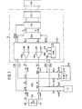
- the telecommunication circuit shown in Fig. 1 includes a line circuit LC which is connected in cascade with a switch circuit HVC between a telecommunication line with conductors LIO and Ll1, connected to a subset TSS, and a switching network SNW.
- LC, HVC and SNW are located in a telecommunication exchange.
- Line circuit LC includes the cascade connection of a SLIC, a Digital Signal Processor DSP, a TransCoder and Filter circuit TCF and a Dual Processor Terminal Controller DPTC.
- Subset TSS includes a normally open hook switch HS connected between the line conductors LIO and U1.
- Switch circuit HVC is for instance of the type disclosed in Belgian patent No. 897 772. It includes 4 pairs of bidirectional switches sw00, sw01 to sw30, sw31 as shown and has line terminals LO and L1 connected to line conductors LIO and LI1 respectively, test terminals TO and T1 connected to a test circuit TC, ringing terminals RGO and RG1 connected to a ringing circuit RC, tip and ring terminals TP and RG connected to the like named outputs of line amplifiers LOAO and LOA1 in the SLIC respectively and terminals STA, STB, SRA, SRB connected to like named terminals of a sensing circuit SENC in the SLIC.
- the line terminals L0/L1 are connected to TP/RG via the series connection of swOO/01, 50 ohms line feed resistors RO/1 and sw10/11 respectively.
- the respective junction points STB and SRA of sw00 and RO and of sw01 and R1 are connected to TC via sw20 and sw21 respectively, whilst the respective junction points STA and SRB of RO and sw10 and of R1 and sw11 are connected to RC via sw30 and sw31 respectively.
- series switches sw00, sw01, sw10 and sw11 are closed, whereas the other shunt switches are open.
- All the switches are controlled by the SLIC so that HVC is able to establish either one of the following connections : between TSS and SLIC (LOAO, LOA1 and SENC); TC and TSS; SLIC (LOAO, LOA1) and TC; RC and TSS; RC and SLIC (SENC).
- the function of TC is to test the connection to TSS and to the SLIC and that of RC is to apply a ringing signal to this line and to SENC in the SLIC.
- RC is able to connect ground through sw30 and the negative battery BA of -48 or -60 Volts in series with a ringing source RS of 90 Volts RMS through sw31.
- the Subscriber Line Interface Circuit SLIC which is integrated on a chip is a two-wire bidirectional circuit on the side of TSS and a four-wire one towards SNW. It has a speech receive input terminal Rx (with ground retum) and a speech transmit output Tx (again with ground retum), Rx and Tx being connected to DSP.
- the SLIC further has a 12 kHz or 16 kHz metering signal input terminal MTCF connected to TCF, data input and output terminals DSP1 and DSP2 connected to DSP and the above mentioned terminals STA, STB, SRA, SRB, TP and RG connected to HVC.
- the sensing circuit SENC included in the SLIC is of the type disclosed in European published application No.
- i the line current comprising a DC component and possibly an AC component constituted by a speech signal and/or a metering signal.
- the digital signal processor DSP converts a digital speech signal received from TCF into an analog speech signal which is then applied to the speech receive terminal Rx of the SLIC. Conversely it converts an analog speech signal received via the speech transmit terminal Tx of the SLIC into a digital version which is applied to TCF.
- DSP also includes an echo canceller circuit.
- ground signalling condition This last condition is called ground signalling condition because it allows signalling in TSS on each of the line conductors by applying a ground thereon. Indeed, because TP and RG are at a low voltage current is able to flow from this ground towards the line circuit;
- DSP2 also receives on its data input terminal DSP2 control data bits transmitted by the SLIC. These bits are the same as those transmitted to DSP1 except that the four bits FR, RNG, CTO and CT1 are respectively replaced by :
- the TCF performs a transcoding operation on digital signals received from the DSP and the DPTC and is also adapted to supply a metering signal MTCF to the SLIC. These operations are described in the Belgian patents 897 771 and 897 773.
- the DPTC performs the general control of the SLIC. Details of this circuit are described in the Belgian patents 898 959 and 898 960.
- circuits TCF and DSP are provided in common for a number of such lines, e.g. 8 lines, as indicated by the multipling arrows.
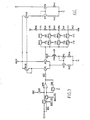
- the output C01 of the sensing circuit SENC is connected to the inputs VEET of both LOAO and LOA1, which have respective feedback resistances R2 and R3, through a DC feedback circuit DCFC which together with the amplifiers LOAO and LOA1, the equal feed resistances RO an R1 and the sensing circuit SENC constitutes a resistance synthesis circuit, i.e. a circuit to convert the value of each of the feed resistances RO and R1 into a wanted resistance value.
- the output C01 of the sensing circuit SENC is also connected via a DC blocking capacitor C1 in series with an amplifier stage OA3 including an operational amplifier, on the one hand to the inverting input INO of LOAO via resistance R4 and, on the other hand, to the non-inverting input N11 of LOA1 through resistance R5 equal to R4.
- the amplifiers LOAO and LOA1, the resistances RO and R1, the sensing circuit SENC, the amplifier stage OA3 and the resistances R4 and R5 constitute an AC impedance synthesis circuit able to convert the resistance value of RO and R1 into a wanted AC impedance.
- the non-inverting inputs NIO of LOAO and Nl1 of LOA1 are connected through equal resistances R6 and R7 to the respective outputs VTI and VRI of a polarity reversal circuit PRC of the type disclosed in the copending Belgian patent application of even date entitled "Polarity reversal circuit".
- the circuit PRC has inputs controlled by the above mentioned drive bits SMPI, HB, BPW, BRO and BR1 and is able to apply a DC supply voltage V+ minus x to VTI and a DC voltage VEET plus x to VRI (normal condition) or vice-versa (reversal condition) or even VEET plus x to both VTI and VRI (ground signalling condition).
- the voltage x is chosen in function of the magnitudes of the speech signal and the metering signal and/or of one or more of the drive bits SMPI, HB, BPW.
- the PRC also provides at its output VX a voltage equal to V + minus 2x which is applied to the DC feedback circuit DCFC.
- the non-inverting input NIO of LOAO and the inverting input IN1 of LOA1 are connected to VAG through respective equal bias resistances R8 and R9.
- the above mentioned outputs MTCF of TCF and Rx of DSP are coupled to the inverting input INO of LOAO and to the non-inverting input NI1 of LOA1 via not shown means (indicated by dashed lines) and respective resistances R10, R11 and R12, R13. R10 and R12 are equal to R11 and R13 respectively.
- the output of the amplifier stage OA3 is also coupled via not shown means (also indicated by a dashed line) to the transmit output Tx.
- the not shown means are without importance for understanding the invention and are for instance of the type disclosed in the above mentioned European patent application.
- the circuit DCFC On the last mentioned output the circuit DCFC generates a regulating voltage VEET which is function of the above line current i and drive bits.
- the current limiting bits CTO and CT1 more particularly control a current limiting circuit CLC which forms part of the DCFC and which will be considered later with reference to Fig. 3.
- the output C01 of the sensing circuit SENC is connected to a circuit controlled by the feed characteristic bit FR and the complement F R thereof. More particularly, this output C01 is connected to the non-inverting input of an operational amplifierOA4 via the series connection, on the one hand of a low pass filter R14, R15, C2 and a transfer gate PG1 and, on the other hand, of a low pass filter R16, C3 and a transfer gate PG2.
- the low pass filter R14, R15, C2 comprises the series resistance R14 and a shunt branch constitued by resistance R15 and capacitance C2 in parallel, whereas the low pass filter R16, C3 comprises the series resistance R16 and the shunt capacitance C3.
- Each of these filters is used to filter the 12 kHz or 16 kHz metering signal from the above mentioned composite AC/DC voltage signal generated at the output C01 of the sensing circuit SENC. Due to the presence of two resistances R14, R15 the filter R14, R15, C2 provides a higher attenuation than the filter R16, C3, as is required in the low ohmic case. This will become clear later. Moreover, these resistances R14 and R15 are external to the chip constituting the SLIC and can therefore be easily replaced by other ones.
- the transfer gates PG1 and PG2 are controlled by bits FR and F R in a reverse way.
- the drive bit FR also controls a PMOS transistor PM1 which is connected in series with a bias resistance R17 between VAG and the inverting input of the amplifier OA4 which has a negative feedback resistance R18.
- the series connection of R17 and PM1 is shunted by a resistance R19.
- transfer gate PG1 is conductive, whereas transfer gate PG2 and transistor PM1 are both blocked.
- the voltage, considered with respect to VAG, and equal to provided at the output of the sensing circuit SENC is attenuated and filtered in the filter circuit R14, R15, C2 and then amplified by a factor equal to 1 +
- R18 R19 so that this factor is then equal to 2.
- transfer gate PG1 is blocked, whereas transfer gate PG2 and transistor PM1 are both conductive.
- the last mentioned voltage is filtered in the filter circuit R16, C3 and then amplified by a factor which is larger than in the low ohmic line condition. In a preferred embodiment so that the gain factor is larger than 5. As will become clear later, this will result in a voltage VEET of higher value and hence in a smaller line current. It should be noted that since in the high ohmic line condition the gain has to be increased, the filter R16, C2 does not include a resistance comparable to R15 and which would decrease this gain.
- the output of amplifier OA4 is connected to a unity gain circuit controlled by the polarity reversal bit BRO and the complement BRO thereof. More particularly, this output is connected via a common resistance R20 and individual PMOS transistors PM2 and PM3 to the non-inverting and inverting inputs of an operational amplifier OA5 respectively. PM2 and PM3 are controlled by the respective bits BRO and BRO. The latter bit BRO also controls PMOS transistor PM4 connected between VAG and the non-inverting input of OAS.
- the latter amplifier OA5 has a negative feedback branch comprising PMOS transistor PM5 and resistance R21 in series, the junction point of PM5 and R31 being connected to the output CL of the current limiting circuit CLC to be considered later.
- the gate of PM5 which is identical to PM3 is connected to the supply voltage V-and PM5 is therefore continuously conductive.
- transistors PM3, PM4 and PM5 are conductive, whereas transistor PM2 is blocked.
- the output voltage, considered with respect to VAG, provided by the amplifier OA5 is amplified by a factor equal to - .
- R20 R21 so that the latter gain factor is equal to -1.
- transistors PM2 and PM5 are conductive, whereas transistors PM3 and PM4 are blocked.
- the voltage, considered with respect to VAG, generated at the output of the amplifier OA5 is amplified by a factor equal to 1.
- the output of amplifier OA5 is connected to the non-inverting input of an operational amplifier OA6 via a filter circuit which comprises series resistances R22 and R23 and shunt capacitance C4.
- the resistance R22 is connected in parallel with the emitter-to-base junction diodes of the diode-connected NPN transistor N1 and PNP transistor P1.
- the purpose of this filter circuit is to filter small residual AC signals, such as speech, as well as to pass to its output large DC signals, such as the one produced when a subscriber goes off hook, substantially without distortion and very rapidly.
- the inverting input of amplifier OA6 is controlled from the output VX of the polarity reversal circuit PRC as well as from a circuit controlled by the battery bit BV and the complement BV thereof.
- the inverting input of OA6 is connected to its output via resistance R24 and the emitter-to-base junction of PNP transistor P2 whose collector is connected to V-.
- the emitter of P2, which constitutes the output VEET is connected to the PRC and to the inputs VEET of both the line amplifiers LOAO and LOA1.
- the circuit controlled by BV and BV includes an operational amplifier OA7 and an associated voltage divider circuit connected between VAUX and VAG and comprising the emitter-to-collector path of PMOS transistor PM6 and resistances R25, R26 and R27 in series.
- the base of transistor PM6 is continuously biased by the constant voltage B1, so that PM6 continuously supplies a constant current to the last mentioned voltage divider.
- the non-inverting input of amplifier OA7 is connected to the bandgap reference voltage B2 and the tapping points TP2 and TP3 of the above voltage divider are connected to its inverting input via respective PMOS transistors PM21 and PM22 which are controlled by the battery bits BV and BV respectively. Tapping point TP1 of this voltage divider is connected to the inverting input of amplifier OA6 via resistance R28.
- the output VX of the polarity reversal circuit PRC is connected to the junction point of three series connected diode connected NPN transistors N2 to N4 and a resistance R29 via the series connection of a resistance R30, the base-to-emitter junctions of NPN transistors N5 and N6 which form a Darlington pair, a resistance R31 and the base-to-emitter junction of a PNP transistor P3 which forms a Common Emitter - Common Collector pair with NPN transistor N7.
- the collectors of N5 and N6 are both connected to the supply voltage V+, and the emitter and collector of transistor P3 are joined to the collector and base of transistor N7 respectively.
- the emitter of the latter transistor N7 is connected to a current source comprising NPN transistors N8, N9 and N10 and resistances R32 and R33. More particularly, this emitter is connected to the supply voltage V-via the collector-to-emitter path of N8 and resistance R32 in series.
- the emitter of N7 is also connected to the base of transistor N9 whose collector-emitter path is connected between VAUX and the base of transistor N8.
- the base of current source transistor N8 is connected to the base of transistor N10 whose emitter is connected to V-via resistance R33 and whose collector is connected to the inverting input of amplifier OA6.
- the voltage at the output VX of the PRC is equal to V + -2x and when calling V(N) the VBE of a transistor N, the voltage at the upper end of resistance R31 is equal to wherein V(R30) is the voltage drop in protection resistance R30.
- the voltage at the lower end of the resistance R31 is eaual to
- the output CLC of filter circuit R16, C3 is also connected, on the one hand to the non-inverting input of operational amplifier OA8 via PMOS transistor PM7 and, on the other hand to the inverting input of OA8 via resistance R34 and PMOS transistor PM8 in series.
- the non-inverting input of OA8 is connected to VAG through bias resistance R35 and its inverting input is connected to its output via PMOS transistor PM9 and resistance R36 in series.
- the gates of transistors PM7 and PM8 are controlled by the Boolean functions 8RO + FR and BRO + F R respectively, whereas the base of transistor PM9 is connected to V-and is therefore continuously conductive.
- transistor PM9 is provided in order to compensate the impedance of PMB.
- the output of amplifier OA8 is connected via a resistance R37 to a first input of a differential amplifier whose other input is connected to tapping points TP4 to TP7 of a voltage divider via the pairs of series connected PMOS transistors PM10, PM11; PM12, PM13; PM14, PM15 and PM16, PM17 controlled by the current limit bits CTO , CTf ; CTO, GTI ; CTO CT1 and CTO, CT1 respeectively.
- the voltage divider comprises resistances R38 to R42 connected in series between bandgap reference voltage B2 and VAG.
- the inputs of the differential amplifier are constituted by the bases of NPN transistors N11 and N12 whose emitters are connected to a common bias current source comprising PMOS transistor PM18, NPN transistors N13 and N14 and resistances R43 and R44.
- the supply source VAUX is connected to V-via the source-to-drain path of PM18 which is controlled by bias source B1, the collector-to-emitter path of diode connected transistor N14 and resistance R44 in series.
- the joined emitters of N11 and N12 are connected to V-via the collector-to-emitter path of current mirror transistor N13 and resistance R43 in series.
- the base of N13 is connected to both the collector and base of N14.
- the collector of N12 is connected to VAUX which is connected to the collector of transistor N11 via the diode connected PMOS transistor PM19 which forms part of a current source/current mirror configuration.
- This configuration further includes PMOS transistor PM20, NPN transistors N15 and N16 and resistances R45 and R46. More particularly, the gate of PM19 is connected to that of PM20 whose source is connected to VAUX and whose drain is connected to V-via the collector-to-emitter path of diode connected transistor N15 and resistance R45 in series.
- the base of transistor N15 is connected to that of transistor N16 whose emitter is connected V-via resistance R46 and whose collector constitutes the output CL of the current limiting circuit CLC and is connected to the junction point of transistor PM5 and resistance R21.
- the circuit just described operates as follows. As long as the input signal applied to the base of transistor N11 is smaller than that applied to the base of transistor N12 and which depends on the value of the current limit bits CTO and CT1, the constant current provided by the current source/current mirror circuit N13, N14, PM18 mainly flows through transistor N12 so that no current flows in the collector-to-emitter path of transistor N16 and that the operation of the circuit including amplifier OA5 is not influenced.
- the function of the circuit R14, R15, C2 is performed by separate filter and voltage divider circuits which are linked by a buffer amplifier in order that the voltage divider circuit should not constitute a load for the filter circuit.
- a drawback of the use of such a buffer amplifier is that it introduces a DC offset in the DC impedance synthesizing loop, that it produces noise and that it occupies a relatively large surface on the chip.
- the circuit R14, R15, C2 has a filter as well as a voltage divider function, so that it may be coupled to the high impedance non-inverting input of operational amplifier OA4 without the use of a buffer amplifier.
- the accuracy of the regulating voltage VEET and therefore of the synthesized DC impedance is increased, the noise factor of the circuit is improved and the required chip surface is decreased.
- the current limiting circuit is controlled from the output of the so-called absolute value circuit including two cascaded amplifiers producing a DC offset and to which the output of the sensing circuit is coupled via a filter circuit.
- the current limiting circuit is directly controlled from the filter circuit output.
Abstract
Description
- The present invention relates to a telecommunication line circuit including line amplifiers whose outputs are coupled to respective line conductors of a telecommunication line via feed resistances, and a resistance synthesis circuit for synthesizing a wanted resistance from said feed resistances, said synthesis circuit having inputs coupled with said feed resistances and an output coupled to supply inputs of said line amplifiers, said output being constituted by the output of an operational amplifier circuit which is controlled by a control voltage and to which said inputs are coupled through a loop current sensing circuit and an AC filter.
- Such a circuit is already known from Belgian patent No. 898049. Therein the control voltage is applied to the non-inverting input of the operational amplifier through a resistance, whilst the filter circuit is coupled to the same input through at least a buffer amplifier in order that this filter circuit should not be loaded by the resistance. Drawbacks of this known circuit are that such a buffer amplifier introduces a DC offset and produces noise so that the accuracy of the DC synthesizing circuit is adversely affected and that noise appears on the line. Moreover, such a buffer amplifier occupies a relatively large surface when the line circuit is integrated on a chip.
- An object of the present invention is to provide a telecommunication line circuit of the above type, but which does not present these drawbacks.
- According to the invention this object is achieved due to the fact that said AC filter is directly connected to the non-inverting input of said operational amplifier circuit whose inverting input is connected to a control circuit to which said control voltage is applied and which is able to transform said control voltage into a control current and to derive this current from said inverting input.
- By transforming the control voltage into a current and deriving it from the inverting input of the operational amplifier, it has been possible to directly connect the filter circuit to the non-inverting input of this amplifier, i.e. without the use of a buffer amplifier. In this way the accuracy of the DC impedance synthesis circuit is increased and the noise performance of the circuit is improved because all unwanted signals are prevented from reaching the line. Also the circuit may be integrated on a smaller chip surface.
- The present invention also relates to an operational amplifier circuit of which an input is coupled via a forward path including a first impedance to at least one of the inputs of an operational amplifier whose inverting input is coupled to the output of the circuit through a feedback path including a second impedance.
- This amplifier circuit is characterized in that said forward and feedback paths include a first and a second number of transistor switches such that the gain of the amplifier circuit is not affected by these switches.
- In this way the effect of the transistor switches required in the forward path of the amplifier is compensated by transistor switches in the feedback path.
- The above mentioned and other objects and features of the invention will become more apparent and the invention itself will be best understood by referring to the following description of a preferred embodiment taken in conjunction with the accompanying drawings wherein :
- Fig. 1 shows a telecommunication circuit including a line circuit according to the invention;
- Figs. 2 and 3 together represent this line circuit in more detail.
- The telecommunication circuit shown in Fig. 1 includes a line circuit LC which is connected in cascade with a switch circuit HVC between a telecommunication line with conductors LIO and Ll1, connected to a subset TSS, and a switching network SNW. LC, HVC and SNW are located in a telecommunication exchange. Line circuit LC includes the cascade connection of a SLIC, a Digital Signal Processor DSP, a TransCoder and Filter circuit TCF and a Dual Processor Terminal Controller DPTC.
- Subset TSS includes a normally open hook switch HS connected between the line conductors LIO and U1.
- Switch circuit HVC is for instance of the type disclosed in Belgian patent No. 897 772. It includes 4 pairs of bidirectional switches sw00, sw01 to sw30, sw31 as shown and has line terminals LO and L1 connected to line conductors LIO and LI1 respectively, test terminals TO and T1 connected to a test circuit TC, ringing terminals RGO and RG1 connected to a ringing circuit RC, tip and ring terminals TP and RG connected to the like named outputs of line amplifiers LOAO and LOA1 in the SLIC respectively and terminals STA, STB, SRA, SRB connected to like named terminals of a sensing circuit SENC in the SLIC. In HVC the line terminals L0/L1 are connected to TP/RG via the series connection of swOO/01, 50 ohms line feed resistors RO/1 and sw10/11 respectively. The respective junction points STB and SRA of sw00 and RO and of sw01 and R1 are connected to TC via sw20 and sw21 respectively, whilst the respective junction points STA and SRB of RO and sw10 and of R1 and sw11 are connected to RC via sw30 and sw31 respectively. As shown for a switched through connection, series switches sw00, sw01, sw10 and sw11 are closed, whereas the other shunt switches are open. All the switches are controlled by the SLIC so that HVC is able to establish either one of the following connections : between TSS and SLIC (LOAO, LOA1 and SENC); TC and TSS; SLIC (LOAO, LOA1) and TC; RC and TSS; RC and SLIC (SENC). The function of TC is to test the connection to TSS and to the SLIC and that of RC is to apply a ringing signal to this line and to SENC in the SLIC. For instance, RC is able to connect ground through sw30 and the negative battery BA of -48 or -60 Volts in series with a ringing source RS of 90 Volts RMS through sw31.
- The Subscriber Line Interface Circuit SLIC which is integrated on a chip is a two-wire bidirectional circuit on the side of TSS and a four-wire one towards SNW. It has a speech receive input terminal Rx ( with ground retum) and a speech transmit output Tx (again with ground retum), Rx and Tx being connected to DSP. The SLIC further has a 12 kHz or 16 kHz metering signal input terminal MTCF connected to TCF, data input and output terminals DSP1 and DSP2 connected to DSP and the above mentioned terminals STA, STB, SRA, SRB, TP and RG connected to HVC. The sensing circuit SENC included in the SLIC is of the type disclosed in European published application No. 85200774.9 and provides at its output a composite DC/AC voltage considered with respect to VAG which is for instance equal to r; a wherein r = RO = R1 and i is the line current comprising a DC component and possibly an AC component constituted by a speech signal and/or a metering signal.
- The digital signal processor DSP converts a digital speech signal received from TCF into an analog speech signal which is then applied to the speech receive terminal Rx of the SLIC. Conversely it converts an analog speech signal received via the speech transmit terminal Tx of the SLIC into a digital version which is applied to TCF. DSP also includes an echo canceller circuit.
- The following drive bits are transmitted by DSP to data input terminal DSP1 of the SLIC :
- -BRO and BR1 : polarity reversal bits indicating that the polarity on RG and on TP has to be made high (1) or low (0) according to the following table :

- This last condition is called ground signalling condition because it allows signalling in TSS on each of the line conductors by applying a ground thereon. Indeed, because TP and RG are at a low voltage current is able to flow from this ground towards the line circuit;
- -FR : a feed characteristic bit to indicate that the synthesized line feed resistance should be high ohmic (0) or low ohmic (1). The meaning of synthesized feed resistance will be explained later;
- -CTO and CT1 : current limit bits indicating four possible maximum line current conditions;
- -BV : a battery bit indicating that the exchange battery V-is -48 Volts (0) or -60 Volts (1);
- -SMPI : a metering signal bit indicating that a metering signal applied to SLIC by TCF has to be allowed in the SLIC (1) or not (0);
- -RNG : a ringing bit indicating that ringing is to be performed (1) or not (0);
- -BPW : a power bit indicating that the SLIC should be put in the power up mode (1) or not (0);
- -HB : a high bias bit indicating that the SLIC should be put in a high bias mode (1) or not (0);
- -RYO, RY1, RY2 : three relay drive bits indicating that a corresponding one of the relays (not shown) having the above mentioned contacts sw00 to sw31 should be operated (1) or not (0).
- Finally, the DSP also receives on its data input terminal DSP2 control data bits transmitted by the SLIC. These bits are the same as those transmitted to DSP1 except that the four bits FR, RNG, CTO and CT1 are respectively replaced by :
- -SHD : a switch hook detection bit indicating that the line loop between SLIC and TSS is open (0) or closed (1 );
- -RT : a ring trip indicating that the ringing signal applied to line by the circuit RC has to be switched off (1) or not (0);
- -OC : an overcurrent or overtemperature bit indicating that the temperature of LOAO and/or LOA1 is above - (1) or below (0) a predetermined value;
- -VPB : a bit indicating that ground detection has to be performed on the line conductors (1) or not (0). In the present case VPB is always 0.
- The TCF performs a transcoding operation on digital signals received from the DSP and the DPTC and is also adapted to supply a metering signal MTCF to the SLIC. These operations are described in the Belgian patents 897 771 and 897 773.
- Finally, the DPTC performs the general control of the SLIC. Details of this circuit are described in the Belgian patents 898 959 and 898 960.
- To be noted that whereas HVC, SLIC and DSP are individually associated to the telephone line, the circuits TCF and DSP are provided in common for a number of such lines, e.g. 8 lines, as indicated by the multipling arrows.
- Reference is now made to Figs. 2 and 3 representing the SLIC of Fig. 1 in more detail. This circuit has some similarities with the one disclosed in Belgian patent no. 898049. This circuit operates with the following voltages :
- V + which is at 0 Volts or ground potential;
- V-which is equal to -48 or -60 Volts e.g. -48 Volts;
- VAUX which is an auxiliary voltage 15 Volts above V-, e.g. -33 Volts;
- VAG which is a voltage half-way between V-and VAUX, i.e. substantially equal to 7,5 Volts above V-, e.g. - 40,5 Volts;
- VEET which is a regulating voltage;
- B1 which is a continuously applied constant voltage equal to about 3 Volts below VAUX;
- B2 which is a so called bandgap reference voltage, e.g. equal to 2.41 Volts above VAG.
- As shown in Fig. 2, the output C01 of the sensing circuit SENC is connected to the inputs VEET of both LOAO and LOA1, which have respective feedback resistances R2 and R3, through a DC feedback circuit DCFC which together with the amplifiers LOAO and LOA1, the equal feed resistances RO an R1 and the sensing circuit SENC constitutes a resistance synthesis circuit, i.e. a circuit to convert the value of each of the feed resistances RO and R1 into a wanted resistance value. The output C01 of the sensing circuit SENC is also connected via a DC blocking capacitor C1 in series with an amplifier stage OA3 including an operational amplifier, on the one hand to the inverting input INO of LOAO via resistance R4 and, on the other hand, to the non-inverting input N11 of LOA1 through resistance R5 equal to R4. The amplifiers LOAO and LOA1, the resistances RO and R1, the sensing circuit SENC, the amplifier stage OA3 and the resistances R4 and R5 constitute an AC impedance synthesis circuit able to convert the resistance value of RO and R1 into a wanted AC impedance.
- The non-inverting inputs NIO of LOAO and Nl1 of LOA1 are connected through equal resistances R6 and R7 to the respective outputs VTI and VRI of a polarity reversal circuit PRC of the type disclosed in the copending Belgian patent application of even date entitled "Polarity reversal circuit". As disclosed in this application the circuit PRC has inputs controlled by the above mentioned drive bits SMPI, HB, BPW, BRO and BR1 and is able to apply a DC supply voltage V+ minus x to VTI and a DC voltage VEET plus x to VRI (normal condition) or vice-versa (reversal condition) or even VEET plus x to both VTI and VRI (ground signalling condition). The voltage x is chosen in function of the magnitudes of the speech signal and the metering signal and/or of one or more of the drive bits SMPI, HB, BPW. The PRC also provides at its output VX a voltage equal to V + minus 2x which is applied to the DC feedback circuit DCFC.
- The non-inverting input NIO of LOAO and the inverting input IN1 of LOA1 are connected to VAG through respective equal bias resistances R8 and R9. The above mentioned outputs MTCF of TCF and Rx of DSP are coupled to the inverting input INO of LOAO and to the non-inverting input NI1 of LOA1 via not shown means (indicated by dashed lines) and respective resistances R10, R11 and R12, R13. R10 and R12 are equal to R11 and R13 respectively. Finally, the output of the amplifier stage OA3 is also coupled via not shown means (also indicated by a dashed line) to the transmit output Tx. The not shown means are without importance for understanding the invention and are for instance of the type disclosed in the above mentioned European patent application.
- The above mentioned DC feedback circuit DCFC which will be described in detail hereinafter has the following terminals :
- -an input connected to the output C01 of the sensing circuit SENC;
- -an input connected to the output VX of the polarity reversal circuit PRC;
- -inputs controlled by the above mentioned drive bits FR, BV, BRO, BR1, CTO and CT1 and by the complements thereof. The function of the other drive bits and of the control bits is not explained in the present description;
- -an output VEET connected to the polarity reversal circuit PRC and to the like named inputs of both the line amplifiers LOAO and LOA1.
- On the last mentioned output the circuit DCFC generates a regulating voltage VEET which is function of the above line current i and drive bits. The current limiting bits CTO and CT1 more particularly control a current limiting circuit CLC which forms part of the DCFC and which will be considered later with reference to Fig. 3.
- The output C01 of the sensing circuit SENC is connected to a circuit controlled by the feed characteristic bit FR and the complement F R thereof. More particularly, this output C01 is connected to the non-inverting input of an operational amplifierOA4 via the series connection, on the one hand of a low pass filter R14, R15, C2 and a transfer gate PG1 and, on the other hand, of a low pass filter R16, C3 and a transfer gate PG2. The low pass filter R14, R15, C2 comprises the series resistance R14 and a shunt branch constitued by resistance R15 and capacitance C2 in parallel, whereas the low pass filter R16, C3 comprises the series resistance R16 and the shunt capacitance C3. Each of these filters is used to filter the 12 kHz or 16 kHz metering signal from the above mentioned composite AC/DC voltage signal generated at the output C01 of the sensing circuit SENC. Due to the presence of two resistances R14, R15 the filter R14, R15, C2 provides a higher attenuation than the filter R16, C3, as is required in the low ohmic case. This will become clear later. Moreover, these resistances R14 and R15 are external to the chip constituting the SLIC and can therefore be easily replaced by other ones. The transfer gates PG1 and PG2 are controlled by bits FR and F R in a reverse way. The drive bit FR also controls a PMOS transistor PM1 which is connected in series with a bias resistance R17 between VAG and the inverting input of the amplifier OA4 which has a negative feedback resistance R18. The series connection of R17 and PM1 is shunted by a resistance R19.
- The circuit just described operates as follows when a low ohmic (FR = 1) or a high ohmic line condition (FR = 0) has to be realised.
- In this case transfer gate PG1 is conductive, whereas transfer gate PG2 and transistor PM1 are both blocked. As a consequence the voltage, considered with respect to VAG, and equal to


- In a preferred embodiment R18 = R19 so that this factor is then equal to 2.
- In this case transfer gate PG1 is blocked, whereas transfer gate PG2 and transistor PM1 are both conductive. As a consequence the last mentioned voltage


- The output of amplifier OA4 is connected to a unity gain circuit controlled by the polarity reversal bit BRO and the complement BRO thereof. More particularly, this output is connected via a common resistance R20 and individual PMOS transistors PM2 and PM3 to the non-inverting and inverting inputs of an operational amplifier OA5 respectively. PM2 and PM3 are controlled by the respective bits BRO and BRO. The latter bit BRO also controls PMOS transistor PM4 connected between VAG and the non-inverting input of OAS. The latter amplifier OA5 has a negative feedback branch comprising PMOS transistor PM5 and resistance R21 in series, the junction point of PM5 and R31 being connected to the output CL of the current limiting circuit CLC to be considered later. The gate of PM5 which is identical to PM3 is connected to the supply voltage V-and PM5 is therefore continuously conductive.
- The circuit just described operates as follows in the normal (BRO = 0) and other (BRO = 1) polarity conditions mentioned above :
- In this case transistors PM3, PM4 and PM5 are conductive, whereas transistor PM2 is blocked. As a consequence the output voltage, considered with respect to VAG, provided by the amplifier OA5 is amplified by a factor equal to -

- In a preferred embodiment R20 = R21 so that the latter gain factor is equal to -1.
- Other conditions (BRO = 1).
- In these cases transistors PM2 and PM5 are conductive, whereas transistors PM3 and PM4 are blocked. As a consequence the voltage, considered with respect to VAG, generated at the output of the amplifier OA5 is amplified by a factor equal to 1.
- It should be noted that the continuously conductive transistor PM5 in the negative feedback path of OA5 is provided in order that its impedance Z should compensate the same impedance of PM3 in the forward path i.e. in the path by which resistance R20 is connected to OAS. Indeed, for instance in the case BRO = 0 the gain factor is in fact equal to


- From the above it follows that the voltage collected from the line is inverted twice, i.e. in SENC and OAS, in the normal condition (BRO = 0) and once in the other conditions (BRO = 1). In this way the signal at the output of amplifier OA5 is independent from the direction of the line current.
- The output of amplifier OA5 is connected to the non-inverting input of an operational amplifier OA6 via a filter circuit which comprises series resistances R22 and R23 and shunt capacitance C4. The resistance R22 is connected in parallel with the emitter-to-base junction diodes of the diode-connected NPN transistor N1 and PNP transistor P1. The purpose of this filter circuit is to filter small residual AC signals, such as speech, as well as to pass to its output large DC signals, such as the one produced when a subscriber goes off hook, substantially without distortion and very rapidly. This is achieved as follows : for a large positively or negatively directed DC voltage variation transistor N1 or PI becomes conductive and short-circuits the resistance R22 due to which the time constant of the filter R22, R23, C4 is reduced so that this voltage variation is rapidly supplied to OA6. On the contrary, for a smaller voltage variation the resistance R22 is not short-circuited so that this variation is more filtered before being supplied to OA6. The voltage applied to the input of OA6 is called V1 + VAG.
- The inverting input of amplifier OA6 is controlled from the output VX of the polarity reversal circuit PRC as well as from a circuit controlled by the battery bit BV and the complement BV thereof. The inverting input of OA6 is connected to its output via resistance R24 and the emitter-to-base junction of PNP transistor P2 whose collector is connected to V-. The emitter of P2, which constitutes the output VEET is connected to the PRC and to the inputs VEET of both the line amplifiers LOAO and LOA1. The circuit controlled by BV and BV includes an operational amplifier OA7 and an associated voltage divider circuit connected between VAUX and VAG and comprising the emitter-to-collector path of PMOS transistor PM6 and resistances R25, R26 and R27 in series. The base of transistor PM6 is continuously biased by the constant voltage B1, so that PM6 continuously supplies a constant current to the last mentioned voltage divider. The non-inverting input of amplifier OA7 is connected to the bandgap reference voltage B2 and the tapping points TP2 and TP3 of the above voltage divider are connected to its inverting input via respective PMOS transistors PM21 and PM22 which are controlled by the battery bits BV and BV respectively. Tapping point TP1 of this voltage divider is connected to the inverting input of amplifier OA6 via resistance R28.
- The circuit just described operates as follows : -in case BV = 0 (battery of -48 Volts) transistors PM21 and PM22 are conductive and blocked respectively so that the reference voltage, say V2 + VAG, applied to the inverting input of amplifier OA6 via resistance R28, is equal to the reference voltage B2, also considered with respect to VAG, multiplied by a gain factor equal to


- The output VX of the polarity reversal circuit PRC is connected to the junction point of three series connected diode connected NPN transistors N2 to N4 and a resistance R29 via the series connection of a resistance R30, the base-to-emitter junctions of NPN transistors N5 and N6 which form a Darlington pair, a resistance R31 and the base-to-emitter junction of a PNP transistor P3 which forms a Common Emitter - Common Collector pair with NPN transistor N7. The collectors of N5 and N6 are both connected to the supply voltage V+, and the emitter and collector of transistor P3 are joined to the collector and base of transistor N7 respectively. The emitter of the latter transistor N7 is connected to a current source comprising NPN transistors N8, N9 and N10 and resistances R32 and R33. More particularly, this emitter is connected to the supply voltage V-via the collector-to-emitter path of N8 and resistance R32 in series. The emitter of N7 is also connected to the base of transistor N9 whose collector-emitter path is connected between VAUX and the base of transistor N8. Finally, the base of current source transistor N8 is connected to the base of transistor N10 whose emitter is connected to V-via resistance R33 and whose collector is connected to the inverting input of amplifier OA6.
- Because the voltage at the output VX of the PRC is equal to V + -2x and when calling V(N) the VBE of a transistor N, the voltage at the upper end of resistance R31 is equal to


- The circuit is now so adjusted, by means of resistance R29 and possibly also by resistance R30, that the VBEs of the transistors are cancelled so that the current I flowing through the resistance R31 is given by

- When calling, as already mentioned :
- V1 + VAG the voltage applied to the non-inverting input of OA6;
- V2 + VAG the reference voltage applied to the inverting input of OA6 via resistance R28,
- one may calculate that the output voltage VEET of OA6 is given by the following relation :


- so that VEET is then given by :

- The current limiting circuit CLC shown in Fig. 3 is now considered.
- The output CLC of filter circuit R16, C3 is also connected, on the one hand to the non-inverting input of operational amplifier OA8 via PMOS transistor PM7 and, on the other hand to the inverting input of OA8 via resistance R34 and PMOS transistor PM8 in series. The non-inverting input of OA8 is connected to VAG through bias resistance R35 and its inverting input is connected to its output via PMOS transistor PM9 and resistance R36 in series. The gates of transistors PM7 and PM8 are controlled by the Boolean functions 8RO + FR and BRO + F R respectively, whereas the base of transistor PM9 is connected to V-and is therefore continuously conductive.
- The circuit just described operates as follows :
- -when FR = 0 (high ohmic line condition) both transistors PM7 and PM8 are blocked and no current limitation is performed;
- -when FR = 1 (low ohmic line condition) the circuit operates either as an inverter (BRO = 0) or as a follower (BRO = 1) in order that in all the conditions (BRO = 1) a signal independent from the direction of the current line should be supplied to the current limiting circuit proper which is connected to the output of amplifier OAB. Indeed :
- -when BRO = 0, transistors PM7 and PM8 are blocked and conductive respectively so that the signal applied to the circuit is multiplied by a gain factor equal to

- -when BRO = 1, transistors PM7 and PM8 are conductive and blocked respectively, so that the gain factor is then equal to 1.
- Again transistor PM9 is provided in order to compensate the impedance of PMB.
- The output of amplifier OA8 is connected via a resistance R37 to a first input of a differential amplifier whose other input is connected to tapping points TP4 to TP7 of a voltage divider via the pairs of series connected PMOS transistors PM10, PM11; PM12, PM13; PM14, PM15 and PM16, PM17 controlled by the current limit bits
CTO , CTf ; CTO,GTI ;CTO CT1 and CTO, CT1 respeectively. The voltage divider comprises resistances R38 to R42 connected in series between bandgap reference voltage B2 and VAG. The inputs of the differential amplifier are constituted by the bases of NPN transistors N11 and N12 whose emitters are connected to a common bias current source comprising PMOS transistor PM18, NPN transistors N13 and N14 and resistances R43 and R44. The supply source VAUX is connected to V-via the source-to-drain path of PM18 which is controlled by bias source B1, the collector-to-emitter path of diode connected transistor N14 and resistance R44 in series. The joined emitters of N11 and N12 are connected to V-via the collector-to-emitter path of current mirror transistor N13 and resistance R43 in series. The base of N13 is connected to both the collector and base of N14. The collector of N12 is connected to VAUX which is connected to the collector of transistor N11 via the diode connected PMOS transistor PM19 which forms part of a current source/current mirror configuration. This configuration further includes PMOS transistor PM20, NPN transistors N15 and N16 and resistances R45 and R46. More particularly, the gate of PM19 is connected to that of PM20 whose source is connected to VAUX and whose drain is connected to V-via the collector-to-emitter path of diode connected transistor N15 and resistance R45 in series. The base of transistor N15 is connected to that of transistor N16 whose emitter is connected V-via resistance R46 and whose collector constitutes the output CL of the current limiting circuit CLC and is connected to the junction point of transistor PM5 and resistance R21. - The circuit just described operates as follows. As long as the input signal applied to the base of transistor N11 is smaller than that applied to the base of transistor N12 and which depends on the value of the current limit bits CTO and CT1, the constant current provided by the current source/current mirror circuit N13, N14, PM18 mainly flows through transistor N12 so that no current flows in the collector-to-emitter path of transistor N16 and that the operation of the circuit including amplifier OA5 is not influenced.
- On the contrary, when due to an increase of the line current, e.g. by a short-circuit, the input signal applied to the base of transistor N11 becomes larger than that applied to the base of transistor N12, the constant current provided by the circuit N13, N14, PM18 mainly flows through transistor N11. It is mirrored in the collector of transistor N16 via transistors PM19, PM20 and N15. As this current is withdrawn from the inverting input of amplifier OA5 less current flows through the feedback resistance R21 thereof so that the output voltage of OA5 is increased. This means that the above mentioned voltage V1 applied to the non-inverting input of amplifier OA6 is also increased and that consequently, as follows from the relation (3), the regulating voltage VEET is increased too. The effect of such an increase is to limit the line current, as required. It is clear from the above that the start of this line current decrease is function of the bits CTO and CT1 which together determine the bias of transistor N12.
- To appreciate the above described circuit the following should be noted. Reference is hereby made to the above mentioned Belgian patent No 898049.
- In the latter patent the function of the circuit R14, R15, C2 is performed by separate filter and voltage divider circuits which are linked by a buffer amplifier in order that the voltage divider circuit should not constitute a load for the filter circuit. A drawback of the use of such a buffer amplifier is that it introduces a DC offset in the DC impedance synthesizing loop, that it produces noise and that it occupies a relatively large surface on the chip. In the circuit, described above the circuit R14, R15, C2 has a filter as well as a voltage divider function, so that it may be coupled to the high impedance non-inverting input of operational amplifier OA4 without the use of a buffer amplifier. Thus the accuracy of the regulating voltage VEET and therefore of the synthesized DC impedance is increased, the noise factor of the circuit is improved and the required chip surface is decreased.
- In the last mentioned Belgian patent use is made of a so-called absolute value circuit including two operational amplifiers (not shown in this patent) to make the DC impedance synthesis independent from the direction of the line current. In the present circuit the same result is achieved by the use of a single amplifier OA5 controlled by the bit BRO. Thus again the present circuit has a better performance than the known one.
- It should also be noted that the present circuit does not affect the DC level of the signals applied to it since these signals are either passed or inverted. This is not the case with the last mentioned absolute value circuit.
- Finally, in the circuit according to the above mentioned Belgian patent, the current limiting circuit is controlled from the output of the so-called absolute value circuit including two cascaded amplifiers producing a DC offset and to which the output of the sensing circuit is coupled via a filter circuit. On the contrary, in the present circuit the current limiting circuit is directly controlled from the filter circuit output.
- While the principles of the invention have been described above in connection with specific apparatus, it is to be clearly understood that this description is made only by way of example and not as a limitation on the scope of the invention.
Claims (18)
Applications Claiming Priority (2)
| Application Number | Priority Date | Filing Date | Title |
|---|---|---|---|
| BE2060894 | 1985-12-20 | ||
| BE2/60894A BE903910R (en) | 1983-10-21 | 1985-12-20 | Telecommunications line circuit with line amplifier - has resistor synthesis circuit and RC filter connected to operational amplifier |
Publications (3)
| Publication Number | Publication Date |
|---|---|
| EP0237656A2 true EP0237656A2 (en) | 1987-09-23 |
| EP0237656A3 EP0237656A3 (en) | 1988-07-27 |
| EP0237656B1 EP0237656B1 (en) | 1992-04-08 |
Family
ID=3865778
Family Applications (1)
| Application Number | Title | Priority Date | Filing Date |
|---|---|---|---|
| EP19860202325 Expired EP0237656B1 (en) | 1985-12-20 | 1986-12-18 | Telecommunication line circuit and amplifier circuit used therein |
Country Status (3)
| Country | Link |
|---|---|
| EP (1) | EP0237656B1 (en) |
| AU (2) | AU589718B2 (en) |
| ES (1) | ES2004501A6 (en) |
Cited By (3)
| Publication number | Priority date | Publication date | Assignee | Title |
|---|---|---|---|---|
| WO1992000643A1 (en) * | 1990-06-26 | 1992-01-09 | Northern Telecom Limited | Line interface circuit |
| WO1993020645A1 (en) * | 1992-04-03 | 1993-10-14 | Northern Telecom Limited | Telephone line interface circuit with voltage switching |
| US5323461A (en) * | 1991-01-31 | 1994-06-21 | Northern Telecom Limited | Telephone line interface circuit with voltage switching |
Family Cites Families (2)
| Publication number | Priority date | Publication date | Assignee | Title |
|---|---|---|---|---|
| US4419995A (en) * | 1981-09-18 | 1983-12-13 | Hochmair Ingeborg | Single channel auditory stimulation system |
| BE898049A (en) * | 1983-10-21 | 1984-04-24 | Bell Telephone Mfg | TELECOMMUNICATION LINE CHAIN AND RELATED VOLTAGE CONVERTER. |
-
1986
- 1986-12-09 AU AU66337/86A patent/AU589718B2/en not_active Ceased
- 1986-12-18 EP EP19860202325 patent/EP0237656B1/en not_active Expired
- 1986-12-19 ES ES8603517A patent/ES2004501A6/en not_active Expired
-
1989
- 1989-08-31 AU AU40883/89A patent/AU613520B2/en not_active Ceased
Cited By (4)
| Publication number | Priority date | Publication date | Assignee | Title |
|---|---|---|---|---|
| WO1992000643A1 (en) * | 1990-06-26 | 1992-01-09 | Northern Telecom Limited | Line interface circuit |
| AU649255B2 (en) * | 1990-06-26 | 1994-05-19 | Northern Telecom Limited | Line interface circuit |
| US5323461A (en) * | 1991-01-31 | 1994-06-21 | Northern Telecom Limited | Telephone line interface circuit with voltage switching |
| WO1993020645A1 (en) * | 1992-04-03 | 1993-10-14 | Northern Telecom Limited | Telephone line interface circuit with voltage switching |
Also Published As
| Publication number | Publication date |
|---|---|
| EP0237656A3 (en) | 1988-07-27 |
| AU589718B2 (en) | 1989-10-19 |
| ES2004501A6 (en) | 1989-01-16 |
| EP0237656B1 (en) | 1992-04-08 |
| AU6633786A (en) | 1987-06-25 |
| AU4088389A (en) | 1989-12-07 |
| AU613520B2 (en) | 1991-08-01 |
Similar Documents
| Publication | Publication Date | Title |
|---|---|---|
| US4041252A (en) | Transformerless two-wire/four-wire hybrid with DC sourcing capability | |
| US4476350A (en) | Battery feed circuit | |
| US4192978A (en) | Operational amplifier hybrid system | |
| EP0503528B1 (en) | Subscriber line interface circuit for ISDN and POTS applications, including echo cancel circuitry | |
| CA1202742A (en) | Loop-start/ground-start line interface circuit | |
| EP0201635B1 (en) | Telecommunication line circuit | |
| US4514595A (en) | Active impedance line feed circuit | |
| EP0212632B1 (en) | Subscriber line interface circuit | |
| US4178485A (en) | Transformerless telephone line circuit | |
| US4472608A (en) | Subscriber line interface circuit | |
| AU644162B2 (en) | Telecommunications line circuit | |
| JP2645022B2 (en) | Subscriber circuit | |
| US6192125B1 (en) | Optical coupling circuit for a data access arrangement (DAA) | |
| EP0237656A2 (en) | Telecommunication line circuit and amplifier circuit used therein | |
| US4538032A (en) | Interface circuit with impedance adaptation means | |
| US4361732A (en) | Trunk interface circuit with current compensation | |
| GB2149618A (en) | Telecommunication line circuit and associated voltage converter | |
| EP0096473B1 (en) | Active impedance line feed circuit | |
| BE903910R (en) | Telecommunications line circuit with line amplifier - has resistor synthesis circuit and RC filter connected to operational amplifier | |
| US4440979A (en) | Current sink for DPT channel unit | |
| EP0241604A2 (en) | Polarity reversal circuit | |
| US4358645A (en) | Loop sensing circuit for use with a subscriber loop interface circuit | |
| US4614840A (en) | Telecommunication line circuit and associated polarity reversal circuit | |
| CA1195446A (en) | Electronic impedance-matched line repeater | |
| BE903911R (en) | Polarity reversing circuit for two telecommunications lines - has reference circuit with outputs coupled to reversing circuit outputs |
Legal Events
| Date | Code | Title | Description |
|---|---|---|---|
| PUAI | Public reference made under article 153(3) epc to a published international application that has entered the european phase |
Free format text: ORIGINAL CODE: 0009012 |
|
| AK | Designated contracting states |
Kind code of ref document: A2 Designated state(s): FR GB IT |
|
| RAP1 | Party data changed (applicant data changed or rights of an application transferred) |
Owner name: ALCATEL N.V. |
|
| RAP3 | Party data changed (applicant data changed or rights of an application transferred) |
Owner name: ALCATEL N.V. |
|
| PUAL | Search report despatched |
Free format text: ORIGINAL CODE: 0009013 |
|
| AK | Designated contracting states |
Kind code of ref document: A3 Designated state(s): FR GB IT |
|
| 17P | Request for examination filed |
Effective date: 19890113 |
|
| 17Q | First examination report despatched |
Effective date: 19910319 |
|
| ITF | It: translation for a ep patent filed |
Owner name: DOTT. ANTONIO SERGI |
|
| GRAA | (expected) grant |
Free format text: ORIGINAL CODE: 0009210 |
|
| AK | Designated contracting states |
Kind code of ref document: B1 Designated state(s): FR GB IT |
|
| ET | Fr: translation filed | ||
| PLBE | No opposition filed within time limit |
Free format text: ORIGINAL CODE: 0009261 |
|
| STAA | Information on the status of an ep patent application or granted ep patent |
Free format text: STATUS: NO OPPOSITION FILED WITHIN TIME LIMIT |
|
| 26N | No opposition filed | ||
| PGFP | Annual fee paid to national office [announced via postgrant information from national office to epo] |
Ref country code: GB Payment date: 19981112 Year of fee payment: 13 |
|
| PGFP | Annual fee paid to national office [announced via postgrant information from national office to epo] |
Ref country code: FR Payment date: 19981113 Year of fee payment: 13 |
|
| PG25 | Lapsed in a contracting state [announced via postgrant information from national office to epo] |
Ref country code: GB Free format text: LAPSE BECAUSE OF NON-PAYMENT OF DUE FEES Effective date: 19991218 |
|
| GBPC | Gb: european patent ceased through non-payment of renewal fee |
Effective date: 19991218 |
|
| PG25 | Lapsed in a contracting state [announced via postgrant information from national office to epo] |
Ref country code: FR Free format text: LAPSE BECAUSE OF NON-PAYMENT OF DUE FEES Effective date: 20000831 |
|
| REG | Reference to a national code |
Ref country code: FR Ref legal event code: ST |
|
| PG25 | Lapsed in a contracting state [announced via postgrant information from national office to epo] |
Ref country code: IT Free format text: LAPSE BECAUSE OF NON-PAYMENT OF DUE FEES;WARNING: LAPSES OF ITALIAN PATENTS WITH EFFECTIVE DATE BEFORE 2007 MAY HAVE OCCURRED AT ANY TIME BEFORE 2007. THE CORRECT EFFECTIVE DATE MAY BE DIFFERENT FROM THE ONE RECORDED. Effective date: 20051218 |