EP0242025A1 - Anisotropic-electroconductive adhesive composition, method for connecting circuits using the same, and connected circuit structure thus obtained - Google Patents
Anisotropic-electroconductive adhesive composition, method for connecting circuits using the same, and connected circuit structure thus obtained Download PDFInfo
- Publication number
- EP0242025A1 EP0242025A1 EP87301263A EP87301263A EP0242025A1 EP 0242025 A1 EP0242025 A1 EP 0242025A1 EP 87301263 A EP87301263 A EP 87301263A EP 87301263 A EP87301263 A EP 87301263A EP 0242025 A1 EP0242025 A1 EP 0242025A1
- Authority
- EP
- European Patent Office
- Prior art keywords
- conductors
- adhesive
- core material
- particles
- electroconductive
- Prior art date
- Legal status (The legal status is an assumption and is not a legal conclusion. Google has not performed a legal analysis and makes no representation as to the accuracy of the status listed.)
- Granted
Links
Images

Classifications
-
- H—ELECTRICITY
- H01—ELECTRIC ELEMENTS
- H01R—ELECTRICALLY-CONDUCTIVE CONNECTIONS; STRUCTURAL ASSOCIATIONS OF A PLURALITY OF MUTUALLY-INSULATED ELECTRICAL CONNECTING ELEMENTS; COUPLING DEVICES; CURRENT COLLECTORS
- H01R4/00—Electrically-conductive connections between two or more conductive members in direct contact, i.e. touching one another; Means for effecting or maintaining such contact; Electrically-conductive connections having two or more spaced connecting locations for conductors and using contact members penetrating insulation
- H01R4/04—Electrically-conductive connections between two or more conductive members in direct contact, i.e. touching one another; Means for effecting or maintaining such contact; Electrically-conductive connections having two or more spaced connecting locations for conductors and using contact members penetrating insulation using electrically conductive adhesives
-
- H—ELECTRICITY
- H01—ELECTRIC ELEMENTS
- H01B—CABLES; CONDUCTORS; INSULATORS; SELECTION OF MATERIALS FOR THEIR CONDUCTIVE, INSULATING OR DIELECTRIC PROPERTIES
- H01B1/00—Conductors or conductive bodies characterised by the conductive materials; Selection of materials as conductors
- H01B1/20—Conductive material dispersed in non-conductive organic material
- H01B1/22—Conductive material dispersed in non-conductive organic material the conductive material comprising metals or alloys
-
- H—ELECTRICITY
- H05—ELECTRIC TECHNIQUES NOT OTHERWISE PROVIDED FOR
- H05K—PRINTED CIRCUITS; CASINGS OR CONSTRUCTIONAL DETAILS OF ELECTRIC APPARATUS; MANUFACTURE OF ASSEMBLAGES OF ELECTRICAL COMPONENTS
- H05K3/00—Apparatus or processes for manufacturing printed circuits
- H05K3/30—Assembling printed circuits with electric components, e.g. with resistor
- H05K3/32—Assembling printed circuits with electric components, e.g. with resistor electrically connecting electric components or wires to printed circuits
- H05K3/321—Assembling printed circuits with electric components, e.g. with resistor electrically connecting electric components or wires to printed circuits by conductive adhesives
- H05K3/323—Assembling printed circuits with electric components, e.g. with resistor electrically connecting electric components or wires to printed circuits by conductive adhesives by applying an anisotropic conductive adhesive layer over an array of pads
-
- H—ELECTRICITY
- H01—ELECTRIC ELEMENTS
- H01L—SEMICONDUCTOR DEVICES NOT COVERED BY CLASS H10
- H01L2224/00—Indexing scheme for arrangements for connecting or disconnecting semiconductor or solid-state bodies and methods related thereto as covered by H01L24/00
- H01L2224/01—Means for bonding being attached to, or being formed on, the surface to be connected, e.g. chip-to-package, die-attach, "first-level" interconnects; Manufacturing methods related thereto
- H01L2224/26—Layer connectors, e.g. plate connectors, solder or adhesive layers; Manufacturing methods related thereto
- H01L2224/28—Structure, shape, material or disposition of the layer connectors prior to the connecting process
- H01L2224/29—Structure, shape, material or disposition of the layer connectors prior to the connecting process of an individual layer connector
- H01L2224/29001—Core members of the layer connector
- H01L2224/29099—Material
- H01L2224/29198—Material with a principal constituent of the material being a combination of two or more materials in the form of a matrix with a filler, i.e. being a hybrid material, e.g. segmented structures, foams
- H01L2224/29298—Fillers
- H01L2224/29299—Base material
- H01L2224/293—Base material with a principal constituent of the material being a metal or a metalloid, e.g. boron [B], silicon [Si], germanium [Ge], arsenic [As], antimony [Sb], tellurium [Te] and polonium [Po], and alloys thereof
-
- H—ELECTRICITY
- H01—ELECTRIC ELEMENTS
- H01L—SEMICONDUCTOR DEVICES NOT COVERED BY CLASS H10
- H01L2224/00—Indexing scheme for arrangements for connecting or disconnecting semiconductor or solid-state bodies and methods related thereto as covered by H01L24/00
- H01L2224/01—Means for bonding being attached to, or being formed on, the surface to be connected, e.g. chip-to-package, die-attach, "first-level" interconnects; Manufacturing methods related thereto
- H01L2224/26—Layer connectors, e.g. plate connectors, solder or adhesive layers; Manufacturing methods related thereto
- H01L2224/28—Structure, shape, material or disposition of the layer connectors prior to the connecting process
- H01L2224/29—Structure, shape, material or disposition of the layer connectors prior to the connecting process of an individual layer connector
- H01L2224/29001—Core members of the layer connector
- H01L2224/29099—Material
- H01L2224/29198—Material with a principal constituent of the material being a combination of two or more materials in the form of a matrix with a filler, i.e. being a hybrid material, e.g. segmented structures, foams
- H01L2224/29298—Fillers
- H01L2224/29399—Coating material
-
- H—ELECTRICITY
- H01—ELECTRIC ELEMENTS
- H01L—SEMICONDUCTOR DEVICES NOT COVERED BY CLASS H10
- H01L2224/00—Indexing scheme for arrangements for connecting or disconnecting semiconductor or solid-state bodies and methods related thereto as covered by H01L24/00
- H01L2224/80—Methods for connecting semiconductor or other solid state bodies using means for bonding being attached to, or being formed on, the surface to be connected
- H01L2224/81—Methods for connecting semiconductor or other solid state bodies using means for bonding being attached to, or being formed on, the surface to be connected using a bump connector
- H01L2224/819—Methods for connecting semiconductor or other solid state bodies using means for bonding being attached to, or being formed on, the surface to be connected using a bump connector with the bump connector not providing any mechanical bonding
- H01L2224/81901—Pressing the bump connector against the bonding areas by means of another connector
- H01L2224/81903—Pressing the bump connector against the bonding areas by means of another connector by means of a layer connector
-
- H—ELECTRICITY
- H01—ELECTRIC ELEMENTS
- H01L—SEMICONDUCTOR DEVICES NOT COVERED BY CLASS H10
- H01L2224/00—Indexing scheme for arrangements for connecting or disconnecting semiconductor or solid-state bodies and methods related thereto as covered by H01L24/00
- H01L2224/80—Methods for connecting semiconductor or other solid state bodies using means for bonding being attached to, or being formed on, the surface to be connected
- H01L2224/83—Methods for connecting semiconductor or other solid state bodies using means for bonding being attached to, or being formed on, the surface to be connected using a layer connector
- H01L2224/838—Bonding techniques
- H01L2224/8385—Bonding techniques using a polymer adhesive, e.g. an adhesive based on silicone, epoxy, polyimide, polyester
- H01L2224/83851—Bonding techniques using a polymer adhesive, e.g. an adhesive based on silicone, epoxy, polyimide, polyester being an anisotropic conductive adhesive
-
- H—ELECTRICITY
- H01—ELECTRIC ELEMENTS
- H01L—SEMICONDUCTOR DEVICES NOT COVERED BY CLASS H10
- H01L2224/00—Indexing scheme for arrangements for connecting or disconnecting semiconductor or solid-state bodies and methods related thereto as covered by H01L24/00
- H01L2224/91—Methods for connecting semiconductor or solid state bodies including different methods provided for in two or more of groups H01L2224/80 - H01L2224/90
- H01L2224/92—Specific sequence of method steps
- H01L2224/921—Connecting a surface with connectors of different types
- H01L2224/9211—Parallel connecting processes
-
- H—ELECTRICITY
- H01—ELECTRIC ELEMENTS
- H01L—SEMICONDUCTOR DEVICES NOT COVERED BY CLASS H10
- H01L2924/00—Indexing scheme for arrangements or methods for connecting or disconnecting semiconductor or solid-state bodies as covered by H01L24/00
- H01L2924/01—Chemical elements
- H01L2924/01019—Potassium [K]
-
- H—ELECTRICITY
- H01—ELECTRIC ELEMENTS
- H01L—SEMICONDUCTOR DEVICES NOT COVERED BY CLASS H10
- H01L2924/00—Indexing scheme for arrangements or methods for connecting or disconnecting semiconductor or solid-state bodies as covered by H01L24/00
- H01L2924/01—Chemical elements
- H01L2924/01079—Gold [Au]
-
- H—ELECTRICITY
- H05—ELECTRIC TECHNIQUES NOT OTHERWISE PROVIDED FOR
- H05K—PRINTED CIRCUITS; CASINGS OR CONSTRUCTIONAL DETAILS OF ELECTRIC APPARATUS; MANUFACTURE OF ASSEMBLAGES OF ELECTRICAL COMPONENTS
- H05K2201/00—Indexing scheme relating to printed circuits covered by H05K1/00
- H05K2201/02—Fillers; Particles; Fibers; Reinforcement materials
- H05K2201/0203—Fillers and particles
- H05K2201/0206—Materials
- H05K2201/0221—Insulating particles having an electrically conductive coating
-
- H—ELECTRICITY
- H05—ELECTRIC TECHNIQUES NOT OTHERWISE PROVIDED FOR
- H05K—PRINTED CIRCUITS; CASINGS OR CONSTRUCTIONAL DETAILS OF ELECTRIC APPARATUS; MANUFACTURE OF ASSEMBLAGES OF ELECTRICAL COMPONENTS
- H05K2201/00—Indexing scheme relating to printed circuits covered by H05K1/00
- H05K2201/02—Fillers; Particles; Fibers; Reinforcement materials
- H05K2201/0203—Fillers and particles
- H05K2201/0206—Materials
- H05K2201/0233—Deformable particles
-
- H—ELECTRICITY
- H05—ELECTRIC TECHNIQUES NOT OTHERWISE PROVIDED FOR
- H05K—PRINTED CIRCUITS; CASINGS OR CONSTRUCTIONAL DETAILS OF ELECTRIC APPARATUS; MANUFACTURE OF ASSEMBLAGES OF ELECTRICAL COMPONENTS
- H05K2201/00—Indexing scheme relating to printed circuits covered by H05K1/00
- H05K2201/06—Thermal details
- H05K2201/068—Thermal details wherein the coefficient of thermal expansion is important
-
- H—ELECTRICITY
- H05—ELECTRIC TECHNIQUES NOT OTHERWISE PROVIDED FOR
- H05K—PRINTED CIRCUITS; CASINGS OR CONSTRUCTIONAL DETAILS OF ELECTRIC APPARATUS; MANUFACTURE OF ASSEMBLAGES OF ELECTRICAL COMPONENTS
- H05K3/00—Apparatus or processes for manufacturing printed circuits
- H05K3/36—Assembling printed circuits with other printed circuits
- H05K3/361—Assembling flexible printed circuits with other printed circuits
-
- Y—GENERAL TAGGING OF NEW TECHNOLOGICAL DEVELOPMENTS; GENERAL TAGGING OF CROSS-SECTIONAL TECHNOLOGIES SPANNING OVER SEVERAL SECTIONS OF THE IPC; TECHNICAL SUBJECTS COVERED BY FORMER USPC CROSS-REFERENCE ART COLLECTIONS [XRACs] AND DIGESTS
- Y10—TECHNICAL SUBJECTS COVERED BY FORMER USPC
- Y10T—TECHNICAL SUBJECTS COVERED BY FORMER US CLASSIFICATION
- Y10T29/00—Metal working
- Y10T29/49—Method of mechanical manufacture
- Y10T29/49002—Electrical device making
- Y10T29/49117—Conductor or circuit manufacturing
- Y10T29/49194—Assembling elongated conductors, e.g., splicing, etc.
Definitions
- This invention relates to an anisotropic-electroconductive adhesive composition for connecting circuits, an adhesive film made from such an adhesive composition, a method for connecting circuits by using these adhesive materials, and a connected circuit structure thus obtained.
- connection of conductors arranged with very fine pitches such as connection of integrated circuits with wiring substrates, connection of display elements with wiring substrates, connection of electric circuits with leads, etc.
- soldering method and a method of using connecting materials such as an electroconductive adhesive, and the like.
- connecting materials since the connecting materials should be formed on only electroconductive portions in these methods, the connection was very difficult in the case of fine circuits with higher density and higher fineness and sometimes adjacent conductors were undesirably connected with such connecting materials.
- connecting materials for connecting conductors have been studied and disclosed in, for example, Japanese Patent Unexamined Publication No. 55-l04007 and U.S. Patent No. 4,ll3,98l, etc.
- Basic ideas of these publications reside in a process for using a so-called anisotropic-electroconductive connecting material wherein a layer of anisotropic-electroconductive connecting material including an electroconductive material such as metal particles is formed between conductors standing opposite to each other, electrical connection between the conductors and electrical insulating properties between adjacent conductors are simultaneously provided by applying pressure or pressure with heating, and the conductors standing opposite to each other are bonded and fixed.
- EP l47856 proposes a process for connecting conductors by melting metal particles dispersed in an insulating adhesive between the conductors. But since the metal particles are melting with heating, the range for connecting conditions is narrow and thus there is a defect in that the reliability at the time of connection is unsatisfactory. That is, even if good connection can be obtained at near the melting point of a metal, but there is a defect in that metal particles flow and are deformed by melting at a temperature higher than the melting point like the conventional soldering to connect adjacent conductors, resulting in losing insulating properties between adjacent conductors (being called "leak") and being unable to apply for fine conductor pitches.
- the rigid metal particles are only present between conductors as mentioned above to make it possible to obtain initial electroconductivity but to make it unsatisfactory to obtain long connection reliability, particularly reliability, for example, in a thermal shock test. Further, it is difficult to control a melting state even at near the melting point from the viewpoint of thermal conductivity and the like. Even if good conductor connecting portions are obtained, since the difference in thermal expansion between an adhesive and the metal particles is large, there is a defect in that the thermal shock resistance is low as mentioned above.
- This invention provides an anisotropic-electroconductive adhesive composition capable of forming connection with high reliability at the time of or after circuit connection overcoming the defects of the prior art, an adhesive film obtained from said adhesive composition, a method for connecting conductors by using these adhesive materials, and a connected conductor structure thus produced and having a low resistance temperature coefficient at conductor connecting portions.
- This invention provides an adhesive composition for connecting conductors and capable of exhibiting anisotropic-electroconductivity by applying pressure comprising 0.l to l5% by volume of electroconductive particles and 99.9 to 85% by volume of electrically insulating adhesive component, each electroconductive particle comprising a polymeric material as a core material and an electrically conductive metal thin layer coated on at least almost the whole surface of said core material, preferably with an aspect ratio of 0.05 to 1.0 and an average particle size of 0.5 to 300 ⁇ m, a ratio of the thermal expansion coefficient of the adhesive component to that of the core material being 0.5/1 to 10/1, and a ratio of the modulus of elasticity in tension of the adhesive component to that of the core material being l.2/l to 0.0l/l.
- This invention further provides an adhesive film for connecting conductors and capable of exhibiting anisotropic-electroconductivity by applying pressure or pressure and heating comprising 0.l to l5% by volume of electroconductive particles and 99.9 to 85% by volume of electrically insulating adhesive component, each electroconductive particle comprising a polymeric material as a core material and an electrically conductive metal thin layer coated on almost whole surface of said core material, preferably with an aspect ratio of 0.05 to l.0 and an average particle size of 0.5 to 300 ⁇ m, a ratio of the thermal expansion coefficient of the adhesive component to that of the core material being 0.5/l to l0/l, and a ratio of the modulus of elasticity in tension of the adhesive component to that of the core material being l.2/l to 0.0l/l.
- This invention still further provides a method for connecting conductors which comprises interposing an adhesive composition or an adhesive film capable of exhibiting anisotropic-electroconductivity by applying pressure or pressure and heating comprising 0.l to l5% by volume of electroconductive particles, each electroconductive particle comprising a polymeric material as a core material, and an electrically conductive metal thin layer coated on almost whole surface of said core material, said electroconductive particles being dispersed in 99.9 to 85% by volume of a [heat sensitive, pressure sensitive, thermosetting and/or photocurable] adhesive component, between electrode conductors standing opposite to each other, and pressing or pressing with heating said circuits so as to make the thickness of the adhesive layer between the circuits in the range of 0.02 to 0.95 of the initial thickness so as to conduct electrical connection and mechanical bonding between the circuits.
- This invention also provides a connected conductor structure comprising conductors standing opposite to each other and connecting materials connecting said conductors mutually electrically, said connecting materials comprising 0.l to l5% by volume of electroconductive particles and 99.9 to 85% by volume of electrically insulating adhesive component, each electroconductive particle comprising a polymeric material as a core material and an electrically conductive metal thin layer coated on almost whole surface of said core material, and said electroconductive particles being fixed between the conductors standing opposite to each other in a deformed state pressed by the conductors.
- Figs. l and 2 are schematic cross-sectional views of the electroconductive particles used in this invention.
- Fig. l the surface of a polymeric core material l is coated with a thin metal layer 2.
- the polymeric core material l has a hollow portion 3.
- the polymeric core materials having structures shown by Fig. l and Fig. 2 are used alone or as a mixture thereof.
- the core material can take any forms of a fully filled body, a hollow body containing a gas such as air therein, a foamed body having cell portions therein, and the like.
- the shape of the polymeric core material l is typically a sphere or sphere-like form and having plastic deformation properties by applying pressure or pressure and heating.
- the polymeric core material may have projections or roughness on the surface, or can be used as agglomerated particles of core material particles.
- polymeric of the polymeric core material means plastics, rubbers, naturally occurring high polymers, a mixture thereof as composites of these materials or copolymers. These polymeric materials may contain one or more crosslinking agents, curing agents and other additives depending on purposes.
- polymers used as the polymeric core material are polyethylenes, polypropylenes, polystyrenes, acrylonitrile-styrene copolymers, acrylonitrile-butadiene-styrene copolymers, polycarbonate, various acrylates such as poly(methyl methacrylate)s, polyvinyl butarals, polyvinyl formals, polyimides, polyamides, polyesters, polyvinyl chlorides, polyvinylidene chlorides, fluorine resins, poly(phenylene oxide)s, poly(phenylene sulfide)s, polymethylpentenes, urea resins, melamine resins, benzoguamine resins, phenol resins, formaline resins, xylene resins, furan resins, diallyl phthalate resins, epoxy resins, polyisocyanate resins, phenoxy resins, silicone resins, etc. These polymeric materials may be modified according to conventional methods. When
- the pressure used for connecting conductors is preferable when it is low so as not to give bad influence to the conductor portions. It is preferable to use the pressure of l00 kg/cm2 or less, more preferably 50 kg/cm2 or less.
- thermal expansion coefficient of the polymeric core material is necessary from the viewpoint of adhesiveness to the coated metal thin layer at the time of thermal deformation.
- thermal expansion coefficient is higher than 20 ⁇ l0 ⁇ 5 (l/°C)
- thermal expansion and shrinkage amounts become so large that the metal thin layer is readily cracked or peeled off.
- the adhesiveness between the metal thin layer and the polymeric core material can be improved by properly selecting a surface activating method such as a plasma or corona treating method, or a surface treating method using various coupling agents, chelating agents, polarity imparting agents, or the like, on the polymeric core material, in addition to consideration of polarity of the polymeric core material and the above-mentioned thermal expansion coefficient.
- a surface activating method such as a plasma or corona treating method, or a surface treating method using various coupling agents, chelating agents, polarity imparting agents, or the like
- metal used as the metal thin layer 2 there can be used various metals, metal oxides and alloys considering the following points:
- metal elements satisfying the above-mentioned conditions (l) and (2) are Zn, Al, Sb, U, Cd, Ga, Ca, Au, Ag, Co, Sn, Se, Fe, Cu, Th, Pb, Ni, Pd, Be, Mg, and Mn. These metal elements can be used alone or as a mixture or alloy thereof. It is possible to add one or more other elements or compounds for special purposes such as for improving hardness, surface tension, etc.
- the metal thin layer 2 can be formed on the polymeric core material l by a physical chemical method such as a vapor deposition method, a sputtering method, an ion plating method, a plating method, or the like; or a chemical method such as a method wherein a small amount of metal is dispersed in a monomer at the time of synthesizing a polymeric core material and the metal powder is adsorbed on polymer particle surfaces after the polymerization, a method wherein a core material having functional groups and a metal is chemically bonded, a method wherein a metal is adsorbed on the core material by using a surface active agent or coupling agent, or the like.
- a physical chemical method such as a vapor deposition method, a sputtering method, an ion plating method, a plating method, or the like
- a chemical method such as a method wherein a small amount of metal is dispersed in a monomer at the time of synthesizing a
- the method for plating the polymeric core material there can be used an electroless plating method conventionally used for forming metal layers.
- the polymeric core material may be subjected to a surface roughening treatment and a hydrophilic treatment, if necessary, and then to a catalyst such as paladium chloride coating step. Then, the polymeric core material is treated in an electroless plating bath at a predetermined temperature such as 20 - 95°C for a predetermined time such as 5 - l20 minutes, if necessary with stirring so as to prevent the agglomeration of the core material.
- the thickness of the plating layer can be controlled by changing the amount of plating solution, plating time, plating temperature, etc.
- nickel plating a nickel-phosphur system or nickel-boron system can be used as a plating solution and sodium hypophosphite, sodium borohydride, or the like can be used as a reducing agent.
- a rochell salt bath, an EDTA (ethylenediaminetetraacetic acid) bath or the like can be used as a plating solution and formaldehyde can be used as a reducing agent.
- a composite metal layer such as a nickel layer + a gold layer, etc. by the plating method.
- a gold layer over a nickel layer
- the use of the substituted type gold plating method is preferable considering the easiness of handling and obtaining the desired thickness.
- the thickness of the metal thin layer is preferably in the range of 0.0l to 5 ⁇ m, more preferably 0.05 to l ⁇ m, and such a thickness can be included in the range of l/5 to l/l000 of the particle size of the electroconductive particles.
- a thickness is preferivelyable so as to reduce the dependency on temperature change, since the electroconductivity is lowered when the thickness is small, and the difference in thermal expansion and shrinkage with respect to the polymeric core material and the adhesive component increases when the thickness is large.
- the metal has sufficient adaptability to deformation due to the thinness of the layer, but it is more preferable to use a metallic material having a large elongation and malleability.
- glass spheres (beads) or glass hollow spheres (balloons) coated with a thin layer of Ag, etc. are used as the electroconductive particles. But since these particles cannot be softened and deformed at the time of pressing with heating, they cannot be used in this invention.
- the electroconductive particles preferably have an average particle size of 0.5 to 300 ⁇ m and an aspect ratio (a ratio of the minimum particle diameter to the maximum particle diameter) of 0.05 to l.0.
- an aspect ratio a ratio of the minimum particle diameter to the maximum particle diameter
- the electroconductive particles preferably have an average particle size of 0.5 to 300 ⁇ m and an aspect ratio (a ratio of the minimum particle diameter to the maximum particle diameter) of 0.05 to l.0.
- the aspect ratio of the electroconductive particles is preferably in the range of 0.05 to l.0 as mentioned above.
- the aspect ratio is outside the above-mentioned range, the particles become too flaky to obtain both the electroconductivity between conductors and insulating properties between adjacent conductors at the same time. Further, there is a strong tendency to lower the adhesiveness to the circuits.
- the electroconductive particles with almost sphere in shape can satisfy the above-mentioned range, but not limited thereto so long as satisfying the above-mentioned conditions. Further, the electroconductive particles may have projections and unevenness on the surface thereof, and may be not only single particle but also agglomerated particles.
- the electroconductive particles are spheres, it is easy to obtain contact of the particles mutually or the particles with conductor surface so as to easily obtain high electroconductivity.
- the electroconductive particles may be present in a single layer at the thickness direction of the connecting material or present in an arrangement of a plurality of particles or in an agglomerated structure.
- Fig. 9 is a schematic cross-sectional view of a connecting material used in this invention.
- numeral ll denotes an electroconductive particle
- numeral l2 an insulating adhesive component
- numeral l9 a polymeric core material
- numeral 20 a metal thin layer.
- the content of the electroconductive particles in the adhesive component is 0.l to l5% by volume.
- the content is less than 0.l% by volume, satisfactory electroconductivity cannot be obtained, while when the content is more than l5% by volume, insulating properties with respect to adjacent conductors are lowered due to an increase of chance for contacting with other particles at the width direction, and transparency of the adhesive film is worsened.
- More preferable range is 0.5 to l0% by volume considering the above-mentioned reasons.
- the adhesive component there can be used heat sensitive, pressure sensitive, thermosetting and/or photocurable adhesives having insulating properties and being used in conventional adhesive sheets.
- the adhesive component preferably has a thermal expansion coefficient of 5 ⁇ l0 ⁇ 4 (l/°C) or less.
- Conventional adhesive sheets comprise a polymer which imparts cohesive force and, if necessary, one or more tackifiers, tackiness regulators, crosslinking agents, anti-aging agents, dispersing agents, etc.
- polystyrene-butadiene block copolymers polystyrene-isoprene block copolymers
- polybutadienes ethyl cellulose, phenoxy resins, polyesters, epoxy resins, polyamides, polyurethanes, natural rubber, synthetic rubbers such as silicone rubbers, and polychloroprenes, polyvinyl ethers, etc.
- tackifier there can be used cyclopentadiene resins, rosin, modified rosins, terpene resins, xylene resins, terpene-phenol resins, alkylphenol resins, coumaron-indene resins, etc., alone or as a mixture thereof, depending on purposes.
- tackiness regulator there can be used various plasticizers such as dioctyl phthalate, etc.
- the crosslinking agent is used for enhancing the cohesive force of the polymer. It is a polyfunctional substance which can react with functional groups of the polymer. Examples of the crosslinking agent are polyiso cyanates, melamine resins, urea resins, phenol resins, amines, acid anhydrides, peroxides, etc. In the case of photocurable polymer, there can be used benzophenone, benzoquinone, etc. as a photosensitizer.
- the anti-aging agent is used when it is necessary to enhance the stability for heat of polymer binder, oxygen, light, and the like.
- examples of the anti-aging agent are stabilizers such as metallic soaps, anti-oxidants such as alkylphenols, ultraviolet absorbing agents such as benzophenones, benzotriazoles, etc. These anti-aging agents may be used alone or as a mixture thereof depending on purposes.
- the dispersing agent is sometimes used for improving dispersing properties of electroconductive particles.
- examples of the dispersing agent are surface active agents of nonionic series, cationic series, anionic series, and ampholytic series. These surface active agents can be used alone or as a mixture thereof.
- the ratio of thermal expansion coefficient of the adhesive component to that of the polymeric core material is 0.5/l to l5/l and the ratio of modulus of elasticity of the adhesive component to that of the polymeric core material is l.2/l to 0.0l/l.
- the thermal expansion coefficient means a linear expansion coefficient at near room temperature and the modulus of elasticity means a modulus of elasticity in tension.
- the above-mentioned ranges are necessary from the viewpoint of connection reliability and long period reliability of the circuit connecting portions.
- the thermal expansion coefficient is outside the above-mentioned range, difference in thermal expansion shrinkage between the polymeric core material and the adhesive component becomes large, the electroconductive particles do not follow the expansion of conductors due to thermal expansion of the adhesive component, resulting in generating undesirably bad contact between the electroconductive particles and the conductors.
- More preferable range is 0.6 to 9 from the same reasons as mentioned above.
- it is necessary to improve the reliability at the time of conductor connection by making the ratio of modulus of elasticity of the polymeric core material almost the same or more as that of the adhesive component.
- the ratio When the ratio is less than 0.0l, the contact of electroconductive particles mutually or electroconductive particles with the conductors easily becomes a point contact which is an insufficient contact at the time of conductor connection due to too high modulus of elasticity of the polymeric core material, which results in producing unsatisfactory electroconductivity.
- the ratio when the ratio is more than l.2, the deformation and flow of the polymeric core material easily take place compared with the adhesive component, so that insulating properties between adjacent conductors cannot be maintained so as to cause leak and cannot be applied to fine conductors. Further, the width of conditions at the time of connection become narrower. More preferable range is l.0 to 0.02 from the same reasons as mentioned above.
- the adhesive composition of this invention can be produced by dissolving the adhesive component comprising a polymer and if necessary one or more additives in a solvent, or dispersing the adhesive component in a medium in a suspended state, or heat melting the adhesive component to give a liquid state, and mixing the electroconductive particles with the liquid adhesive component by a conventional dispersing method using a ball mill, a stirring apparatus, or the like.
- a solvent since the electroconductive particles having the metal thin layer on the polymeric core material have little solubility in a solvent, it is possible to use a solvent. It is more preferable to select a solvent which can dissolve the adhesive component but does not dissolve the polymeric core material. Examples of such a solvent are toluene, methyl ethyl ketone, dioxane, ethyl acetate, etc. It is also a good method wherein the adhesive is emulsified and then the electroconductive particles are dispersed in an aqueous medium.
- the adhesive composition containing the electroconductive particles can be coated directly on one or both conductors to be connected by means of screen printing or using a roll coater to form adhesive layers, or can be formed into a film-like continuous long sheet.
- the adhesive film in the form of continuous long sheet can be produced by forming a connecting material layer on a separator made of paper or plastic film treated with release treatment depending on necessity by means of screen printing or using a roll coater, followed by continuous wind-up. When the adhesive layer has no stickiness, it is possible to wind up the adhesive film without using the separator. Further, it is possible to use a core material such as non-woven fabric for reinforcing the adhesive.
- the thickness of the adhesive film can be determined considering the particle size of electroconductive particles and properties of connecting material. Preferable thickness is l to 300 ⁇ m. When the thickness is less than l ⁇ m, sufficient adhesiveness cannot be obtained, while when the thickness is more than 300 ⁇ m, a larger amount of electroconductive particles are necessary in order to obtain sufficient electroconductivity; this is not preferable from the viewpoint of practical use. More preferable thickness is 3 to l00 ⁇ m by the same reasons as mentioned above.
- the thus obtained adhesive film has considerable transparency.
- the adhesive film has transparency, quality control during the production is easy and the adhesive film has good surface appearance. Further, in the case of adhesion of display elements, it is possible to take a structure wherein an adhernd can be seen through.
- Connection of conductors can be carried out by preliminarily adhering the adhesive film to conductors, and if a separator is present, the separator is peeled off, or coating the adhesive composition on conductors, and if necessary removing a solvent, and then placing another conductors to be connected on the adhesive tape or adhesive composition, followed by bonding by a heat press, a heat roll, or the like.
- Figs. 3 and 4 are schematic cross-sectional views showing a connected state of conductors by using the adhesive film of this invention. Since the adhesive 4 is softened and flowed by the heat and pressure and at the same time the electroconductive particles 8 are softened and flowed to contact mutually, electroconductive adhesion between the conductors 5 and 6 becomes possible.
- numeral 7 denotes an insulating substrate.
- Fig. 3 shows an example wherein electroconductive particles 8 are present in double or more layers between conductors 5 and 6. Such a structure can give high electroconductivity, since the metal layers on the particle surfaces contact each other to form electroconductive paths.
- the coating metal layer is so thin that it can sufficiently follow the deformation of the polymeric core material. Even if it cannot follow the deformation of the polymeric core material and defects such as cracks may be formed on the coating metal thin layer, the electroconductive path can be maintained by contact with conductors or other particles.
- the ratio t/T 0.02 to 0.95, wherein T is the thickness of the adhesive composition (or film) before the connection and t is the thickness between the conductors after connected.
- the ratio of d/D can be used in place of the ratio of t/T.
- the ratio of t/T When the ratio of t/T is less than 0.02, there is a tendency to destroy the electroconductive particles and to easily drop the metal thin layer. On the other hand, when the ratio is more than 0.95, a sufficient areal contact of conductor with electroconductive particles or contact of electroconductive particles each other cannot be obtained, which results in failing to obtain satisfactory connection reliability.
- Preferable range of the ratio of t/T is 0.l0 to 0.90 by the same reasons as mentioned above.
- the spacer particles it is necessary to use those having higher rigidity than the electroconductive particles. That is, it is necessary that the spacer particles hardly show changes in the particle shape by the pressing or pressing with heating at the production of the connected conductor structure.
- the spacer particles may be either electroconductive or insulating, or a mixture of these spacer particles may also be used.
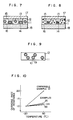
- Figs. 7 and 8 are schematic cross-sectional views of connected conductor structures of this invention.
- the electroconductive particles ll are dispersed in an insulating adhesive component l2 and are interposed between a conductor l3 formed on a substrate l7 and a conductor l4 formed on a substrate l8, and are so arranged as to form areal contact between electroconductive particles mutually or between electroconductive particles and conductor faces with suitable deformation in a pressed state along the conductor surfaces when subjected to pressing or pressing with heating at the time of conductor connection.
- the non-conductor portions l5 and l6 since electroconductive particles are not pressed as those between the conductors, no deformation takes place. Therefore, insulating properties with respect to adjacent circuits can sufficiently be maintained in addition to the selection of the particle size and adding amounts of electroconductive particles.
- the metal coated on the polymeric core material forms an electroconductive path by contacting mutually with other electroconductive particles or with electroconductive conductors under pressure or pressure with heating at the time of connection.
- the polymeric core material can be softened or deformed at the time of connection operation under pressure or pressure with heating, it is possible to maintain the large contact area by properly deforming with pressing the conductor surfaces or electroconductive particles mutually, resulting in obtaining good electroconductivity and reliability.
- the insulating properties with regard to adjacent circuits can sufficiently be maintained, when the selection of the particle size and adding amount of electroconductive particles are also considered as well.
- connection conditions in a very wide range.
- amorphous polymers showing no definite melting points or crosslinked polymers having a wide rubber-state region are used as the core material, it is possible to take the conductor connection conditions (temperature, pressure, time, etc.) very wide, since their softening flow regions (until glass state - rubber state - liquid state regions) are wide. As a result, reliability at the time of connection is remarkably improved and the connection workability is also bettered.
- the degree of softening deformation of the polymeric core material can be set properly depending on their connecting conditions, so that it is possible to control the connecting state. For example, even if the particle size of electroconductive particles at the connecting portions is uneven, it is possible to press a larger electroconductive particle 8 to the size of a smaller electroconductive particle 8′ or less as shown in Fig. 4 by controlling the connecting conditions so as to obtain good connection. Thus, the electroconductive particles can contribute to the electroconductivity effectively. In contrast, in the case of prior art metal particles as shown in Fig. 5, a larger electroconductive particle 9 functions as a spacer and a smaller electroconductive particle 9′ does not contribute to the electroconductivity. Therefore, the number of electroconductive points are reduced to lower the connection reliability.
- the polymeric core material has a thermal expansion coefficient similar to that of the adhesive component, the adaptability to the temperature change after connection are high and long term connection reliability representative by thermal shock resistance is excellent.
- the conductor connection portion according to this invention When the conductor connection portion according to this invention is subjected to a temperature change, stress is acted between the circuits 5 and 6 so as to separate each other by thermal expansion and shrinkage at the direction of y axis by the adhesive component 4 which has a relatively larger thermal expansion coefficient than the materials of the circuits 5 and 6. Since the thermal expansion coefficient of the polymeric core material l and that of the adhesive component 4 are very close, and the metal layer 2 is sufficiently thin, sufficient deformation at the thickness direction of the conductors 5 and 6 is possible and thus the electroconductive connection of the conductors can be maintained well. In this time, the adhesive component 4 is also to show thermal expansion and shrinkage at the direction of x axis. But since the modulus of elasticity of the adhesive component 4 is relatively sufficiently small compared with metallic conductors, the deformation is substantially inhibitted. Further, since the modulus of elasticity is small, the thermal stress is easily relaxed.
- connected conductor structure since the electroconductive particles can be properly deformed when pressed along the conductor surfaces so as to maintain the contact area large, it is possible to effectively maintain the contact area of, for example, a transparent electroconductive film, which was impossible to be soldered according to a prior art technique. Further, it is not particularly necessary to conduct a surface treatment such as Au or Ni plating on the transparent electroconductive film.
- connected circuit structures can also be obtained as to other various conductor surfaces such as Sn, Cr, solder, etc.
- the contact area with the conductors can be taken large and the thermal expansion coefficients of the polymeric core material and the adhesive component are very similar, broadening of the distance between the connected conductors can be solved without giving any influences by thermal expansion.
- the contact state between the electroconductive particles and the conductors can be maintained well, and the resistance change against the temperature change at the connecting portion can be reduced to remarkably small.
- Electroconductive particles coated with Au and having different coating layer thickness as shown in Table l were prepared by using as a polymeric core material Finepearl (a trade name of polystyrene spherical particles, manufactured by Sumitomo Chemical Co., Ltd., specific gravity l.05) having different average particle sizes and by an electroless plating method comprising the following steps (a) to (e).
- Finepearl a trade name of polystyrene spherical particles, manufactured by Sumitomo Chemical Co., Ltd., specific gravity l.05
- a polymeric core material was stirred compulsorily in methanol and subjected to a pretreatment including both degreasing and roughening followed by separation of the methanol by filtration.
- the polymeric core material was dispersed in 200 ml of Circuit Prep 33l6 (a trade name for an activation treating solution comprising PdCl + HCl + SnCl2, manufactured by Japan Electroplating Engineers Co., Ltd.) and stirred at 25°C for 20 minutes for activation, followed by washing with water and filtration.
- Circuit Prep 33l6 a trade name for an activation treating solution comprising PdCl + HCl + SnCl2, manufactured by Japan Electroplating Engineers Co., Ltd.
- the polymeric core material subjected to the activation treatment was immersed in a solution of Blue Sumer (a trade name for an electroless Ni plating solution, manufactured by Japan Kanigen Co., Ltd., bath capacity 300 ⁇ dm2/l) and stirred compulsorily at 90°C for 30 minutes.
- Blue Sumer a trade name for an electroless Ni plating solution, manufactured by Japan Kanigen Co., Ltd., bath capacity 300 ⁇ dm2/l
- the plating solution amount was calculated from the surface areas of the particles.
- the substitution plating of Au was carried out to give electroconductive particles having an Au coating (thickness 0.l ⁇ m) over Ni surfaces.
- the plating solution Lectroles Prep (a trade name for an electroless gold plating solution, manufactured by Japan Electroplating Engineers Co., Ltd.) was used. The plating treatment was conducted at 90°C for l0 minutes, followed by sufficient washing with water and drying at 80°C for 2 hours.
- Adhesive compositions containing electroconductive particles were prepared by adding polystyrene spherical particles coated with Au plating with the particle size and the coating plating layer thickness as listed in Table l to an adhesive solution comprising l00 parts of styrene-butadiene block copolymer (MI 2.6 TAFUPLEN, a trade name, mfd. by Asahi Chemical Co., Ltd.), 40 parts of a terpene series tackifier (CLEARON P-l25, a trade name, mfd. by Yushi Kogyo Co., Ltd.) and 200 parts of toluene in amounts as listed in Table l, followed by ultrasonic dispersion.
- MI TAFUPLEN a trade name, mfd. by Asahi Chemical Co., Ltd.
- a terpene series tackifier CLARON P-l25, a trade name, mfd. by Yushi Kogyo Co.,
- Each adhesive composition obtained as mentioned above was coated on a separator (a polyester film treated with silicone) by using a bar coater and dried at l00°C for 5 to 30 minutes depending on thickness to remove the solvent and to obtain an adhesive film.
- Table l The evaluation results are shown in Table l. In each Example, since each adhesive sheet has transparency, the positioning of conductors was easy. Table l also shows properties of connected conductor structures. The connected structures obtained in individual Examples showed good electroconductive resistances and good insulating properties with respect to adjacent conductors. These properties were still good after reliability test.
- Examples l to 9 The process of Examples l to 9 was repeated except for the kinds of electroconductive particles were changed. That is, in Examples l0 and ll, epoxy spherical particles (TORAYPEAL, a trade name, mfd. by Toray Industries, Inc.) were used as the polymeric core material and a Cu layer with 0.2 ⁇ m thick was formed on the core particles and a Ni layer with 0.2 ⁇ m thick was formed thereon to give a complex layer of metals. In Examples l2 and l3, an Au layer with 0.2 ⁇ m thick was formed on an epoxy sperical particle. As the plating solutions, those of Ni and Au used in Examples l to 9 were used.
- TORAYPEAL epoxy spherical particles
- Cu plating solution there was used Circuit Prep (a trade name for an electroless copper plating solution, mfd. by Japan Electroplating Engineers Co., Ltd.). The electroless plating was carried out at 30°C for 30 minutes.
- the adhesive component and the evaluation were the same as described in Examples l to 9. The evaluation results were shown in Table l. In each Example, good properties were obtained at initial stage and after evaluation of reliability.
- Films were prepared and evaluated in the same manner as described in Examples l to l3 except for changing the kinds of electroconductive particles. That is, as the electroconductive particles, there were used atomized Ni spheres coated with Au (Comparative Example 2), glass spheres coated with Ag (Comparative Example 3), and solder particles having a melting point of l50°C (Comparative Example 4).
- the atomized Ni spheres was available from Takeuchi Metal Foil & Powder Engineering Co., Ltd., the glass spheres were available from Toshiba Ballotini Co., Ltd. and the solder particles were available from Nippon Genma Co., Ltd.
- the Au coating was conducted by using the same electroless Au plating solution as used in Examples l to 9. Further, the electroless Ag plating was conducted by using ALGNA-ET (a trade name, mfd. by Degussa Co., Ltd., in West Germany) at room temperature.
- Electroconductive particles were obtained by coating (sputtering as described in Japanese Patent Unexamined Publication No. 56-l30469) spherical particles of acrylonitrile-butadiene rubber (NBR) (Nipol DN 2l4, a trade name, mfd. by Japanese GEON Co., Ltd., acrylonitrile content 33%, Mooney viscosity 78) with Al by vapor deposition.
- NBR acrylonitrile-butadiene rubber
- transparent electroconductive glass having a conductor with the same pitches as the FPC and 0.5 mm thick was press bonded thereto between a pair of rolls under conditions of 25°C - 5 kg/cm2 - 2 seconds
- Example l4 a rise in resistance value in the reliability test was relatively large, but within the range causing no problem in practical use.
- Example l6 Higher level of the resistance values in Examples l4 to l6 than Examples l to l3 seems to be drived from containing conductor resistance of transparent electroconductive glass. In Example l6, the ultraviolet light was irradiated from the glass conductor side.
- the coating of a polymeric core material was carried out by using the same Ag plating solution as used in Comparative Example 3 and plating of Ag in 0.2 ⁇ m thick.
- a powdery polyimide mfd. by Rhone-Poulenc S.A.
- a thermoplastic polyester BYRON 300, a trade name, mfd. by TOYOBO Co., Ltd., molecular weight ( n) about 20,000, Tg 7°C
- the same NBR as used in Examples l4 to l6 was used.
- the same acrylic rubber as used in Examples l4 to l6 was used as the adhesive component.
- polyester the same thermoplastic polyester as used for the polymeric core material was used.
- polymeric core materials there were used those of 270 mesh pass and 325 mesh on in Examples l7 and l8, and those of l50 mesh pass and l70 mesh on in Example l9.
- Example l9 FPC (Cu thickness, 35 ⁇ m) having conductors of a pitch of 0.4 mm (circuit width 0.2 mm) and transparent electroconductive glass was used.
- Comparative Example 5 there was taken a combination of the polymeric core material having a larger thermal expansion coefficient and a smaller modulus of elasticity than the adhesive component. But when heated so as to flow the adhesive component, leak was generated due to greater flowability of the polymeric core material.
- Example 20 the adhesive composition was heated at l90°C and film casted between heated rolls to produce a film by hot melt coating, followed by preliminary adhesion to an FPC.
- Example 2l an adhesive composition dissolved in a solvent (30% solution of methyl ethyl ketone, in this case) as in Examples l to 9 was directly coated on an FPC by silk screen printing, followed by removal of the solvent by drying to give the FPC having thereon the adhesive composition.
- the FPC having pitches of l.27 mm (Cu foil conductors with width 0.635 mm, and circuit thickness 35 ⁇ m) was used.
- Example 20 As is clear from Table 3, good properties are obtained in Examples 20 and 2l. In Example 20, since no solvent was used, the working circumstances were good. In Example 2l, since the adhesive composition was directly coated on the conductor, it was not necessary to conduct a preliminary adhesion operation at the time of circuit connection. Further, it was impossible to measure a total light transmittance of only the adhesive composition layer, but since the adhesive composition layer had the same transparency as in Example 2l after preliminary adhesion to the FPC, the registering of conductors was easy.
- Table 4 shows combinations of the polymeric core materials and adhesive components used in the above-mentioned Examples and Comparative Examples and properties of these materials (thermal expansion coefficients and modulus of elasticity). As shown in Table 4, better results were obtained when the ratio of thermal expansion coefficients (adhesive component/electroconductive particles) is 0.66 to 8.93 and the ratio of modulus of elasticity (adhesive component/electroconductive particles) is 0.02 to l.2.
- Example ll Using the adhesive film obtained in Example ll and the same combination of conductors as in Example l4 (FPC/transparent electroconductive glass, pitch 0.2 mm), influences by connection conditions were examined.
- Example 24 since the distance between the circuits was reduced to 3 ⁇ m which value was the same as the average particle size of the electroconductive particles, the contact points and contact areas with the conductors were remarkably increased. In Example 25, since individual electroconductive particles were sufficiently pressed and deformed in a single particle layer, the contact areas with the conductors were further increased.
- Example l2 Using the adhesive film obtained in Example l2 and the same combination of circuits as in Examples 22 to 25 (FPC/transparent electroconductive glass), influences by connection conditions were examined.
- Reliability was evaluated by subjecting a pair of conductors connected by using an adhesive film or the like to l0 cycles of a thermal shock test, one cycle comprising -40°C for 30 minutes/+l00°C for 30 minutes, measuring resistance and compared with an initial resistance value.
- the thermal shock test is the most important and reliable test method as a practical test, since it can estimate the length of life by the evaluation in a short time with the most severe conditions.
- Total light transmittance was measured according to JIS K-67l4 using a digital turbidimeter NDH-20D manufactured by NIPPON DENSHOKU Co., Ltd.
- a specimen was prepared by pressing with heating or a solvent removal method in the case of a thermal reactive system to give a sheet of about 500 ⁇ m thick.
- the thermal expansion coefficient was measured by using a thermal mechanical analyser (TMA-l500 manufactured by SHINKU RIKOU Co., Ltd.).
- the modulus of elasticity was measured by using this specimen with a Tensilon UTM-l manufactured by TOYO BALDWIN Co., Ltd. according to ASTM D882-64T.
- Electroconductive particles having an average particle size of 20 ⁇ m were prepared by coating Au, Ag or Ni layers by an electroless plating method on the surfaces of the same epoxy resin particles as used in Examples l0 to l3 used as the polymeric core material.
- the thickness of each metal layer was 0.2 ⁇ m.
- thermoplastic polyester BYRON 300, a trade name, mfd. by TOYOBO Co., Ltd., molecular weight ( n ) 20,000, Tg 7°C
- alkylphenol resin HITANOL 2400, a trade name, mfd. by HITACHI Chemical Co., Ltd., softening point l00°C
- the adhesive solution was mixed with the electroconductive particles mentioned above, coated on a separator (silicone treated polyester film) with a bar coater, and dried at ll0°C for 5 minutes to give a film-like connecting material having 5% by volume of the electroconductive particles and a thickness of 25 ⁇ m.
- a connecting material of connecting width of 3 mm and length of l00 mm was placed and pressed with heating at l50°C and a pressure of l0 kg/cm2 for 5 seconds for preliminary bonding to give a connecting material attached FPC.
- the separator was peeled off, and transparent electroconductive glass (indium oxide circuit, glass thickness l mm) having the same pitch as the FPC was placed thereon so as to register the conductors under a microscope and pressed with heating at l70°C under a pressure of 20 kg/cm2 for l0 seconds for conductor connection.
- transparent electroconductive glass indium oxide circuit, glass thickness l mm
- connection resistance of the conductors at -20°C and +80°C was measured by using a Multimeter and insulating properties between adjacent conductors were also checked. Insulating properties were evaluated as good when the value was l07 ⁇ or more. Measured results of the resistance were expressed by a changing rate of resistance at 80°C taking the value at -20°C as l.0.
- Examples 33 to 35 were repeated except for using solder particles having a particle size of 20 ⁇ m and a melting point of l70°C without polymeric core material as the electroconductive particles.
- the adhesive film preparation and evaluation thereof were carried out in the same manner as described in Example 36 except that at the preparation of the connecting material atomized Ni (mfd. by Fukuda Metal & Powder Co., Ltd., average particle size l0 ⁇ m, almost spherical) was added in addition to the Ni coated polystyrene particles.
- atomized Ni mfd. by Fukuda Metal & Powder Co., Ltd., average particle size l0 ⁇ m, almost spherical
- Example 37-2 and 37-4 the thickness after conductor connection was controlled by the particle size (l0 ⁇ m) of the electroconductive Ni particles which were used as the spacer particles.
- the electroconductive spacer having the smaller particle size than that of electroconductive particles made from polymeric core material, the electroconductive particles made from polymeric core material were present between the conductors in a slightly pressed state together with Ni particles to obtain a preferable connection state.
- Example 37-l wherein connection was carried out at l30°C, the thickness between the conductors was l8 ⁇ m which was larger than the spacer particle size of l0 ⁇ m, since flowability of both the polymeric core material and the adhesive component was insufficient.
- the temperature is to be raised higher or other means, it is possible to control the thickness to the spacer particle size.
- Example 37 The process of Example 37 was repeated except for using an insulating silica powder (ELSIL, a trade name, mfd. by Japan Aerosil Co., Ltd., particle size l0 ⁇ , sperical) in place of atomized Ni as the spacer particles.
- ELSIL insulating silica powder
- Example 38 The process of Example 38 was repeated except for using particles having an average particle size of 3 ⁇ m (the Ni coating layer having a thickness of 0.l ⁇ m) as the electroconductive particles so as to give a film-like connecting material of l5 ⁇ m thick and containing 2% by volume of the electroconductive particles.
- This Example corresponds to the use of spacer particles having a larger particle size than the electroconductive particles.
- the softened deformation region of the polymeric core material is sufficiently large compared with a metal having a constant melting point, it becomes possible to employ wider conditions for conductor connection operation, resulting in improving the reliability at the time of connection.
- the thermal expansion coefficient of the polymeric core material is close to that of the adhesive component, even if the distance between the connecting conductors becomes large due to the thermal expansion of the adhesive component, good contact state between the particles and the conductors can be maintained by the thermal expansion of the electroconductive particles.
- control of connecting state can be carried out by a relatively easy method such as a thickness measurement.
- the adhesive film has transparency, registration of fine conductors can easily be carried out by an aid of transmitting light.
- this invention is very significant from the viewpoint of saving resourses.
- electroconductive particles which comprise polymeric core materials and coated thereon metal thin layers having electroconductivity are used, they can properly be softened or deformed between conductor surfaces or by electroconductive particles mutually by pressing or pressing with heating at the time of conductor connection, so as to maintain the contact area large.
- the polymeric core material has rigidity and thermal expansion and shrinkage properties very close to those of the adhesive component compared with prior art metal particles and can follow the deformation of the adhesive component due to thermal expansion and shrinkage depending on temperature changes, it is possible to make the connected conductor structure small in resistance change.
- the polymeric core materials can take a structure wherein the electroconductive metal thin layers are present in compressed form in contact with conductor surfaces due to the elasticity of the polymeric core materials, they have no selectivity for conductor materials such as transparent electroconductive films. Thus it becomes possible to obtain effective connected conductor structures excellent in reliability using a non-treated transparent electroconductive film which required a special surface treatment according to a prior art technique.
- the core material of electroconductive particles is a polymer
- a wide range of connecting conditions can be employed due to wide range of softening and deformation of the polymer, which results in providing stable connected conductor structures with little deviation.
- the connected conductor structure of this invention uses metals effectively in its electroconductive particles, this invention is also significant from the viewpoint of saving resources.
Abstract
Description
- This invention relates to an anisotropic-electroconductive adhesive composition for connecting circuits, an adhesive film made from such an adhesive composition, a method for connecting circuits by using these adhesive materials, and a connected circuit structure thus obtained.
- As methods for connecting conductors arranged with very fine pitches such as connection of integrated circuits with wiring substrates, connection of display elements with wiring substrates, connection of electric circuits with leads, etc., there have widely been used a soldering method, and a method of using connecting materials such as an electroconductive adhesive, and the like. But, since the connecting materials should be formed on only electroconductive portions in these methods, the connection was very difficult in the case of fine circuits with higher density and higher fineness and sometimes adjacent conductors were undesirably connected with such connecting materials.
- Recently, connecting materials for connecting conductors have been studied and disclosed in, for example, Japanese Patent Unexamined Publication No. 55-l04007 and U.S. Patent No. 4,ll3,98l, etc. Basic ideas of these publications reside in a process for using a so-called anisotropic-electroconductive connecting material wherein a layer of anisotropic-electroconductive connecting material including an electroconductive material such as metal particles is formed between conductors standing opposite to each other, electrical connection between the conductors and electrical insulating properties between adjacent conductors are simultaneously provided by applying pressure or pressure with heating, and the conductors standing opposite to each other are bonded and fixed.
- But in these methods, since the electrical conduction between the conductors was obtained mainly by contact of a plurality of electroconductive materials such as metal particles in many cases, the contact areas between particles or between a particle and a conductor surface was insufficient due to rigidity of metal particles and reliability of conduction was insufficient.
- On the other hand, in order to improve the initial connection reliability or to reduce the production cost using the same idea for electrical conduction as mentioned above, there have been proposed methods for obtaining anisotropic-electroconductive connection by using particles having electroconductive layers on the surfaces of electroconductive particles or insulating particles which were used as core materials (e.g. Japanese Patent Unexamined Publication Nos. 56-l22l93, and 58-lll202). But when metal particles, alumina, glass and the like were used as the core material, the contact areas between particles or a particle and a conductor surface were insufficient due to the rigidity of core materials and thus the reliability of conduction was unsatisfactory.
- The above-mentioned prior art technics make it possible to obtain anisotropic electroconductivity at the time of conductor connection, but cannot provide reliability at the connected portion for practical use. This is shown by Comparative Examples l to 4 in Table l mentioned below.
- In order to improve the connection reliability, EP l47856, for example, proposes a process for connecting conductors by melting metal particles dispersed in an insulating adhesive between the conductors. But since the metal particles are melting with heating, the range for connecting conditions is narrow and thus there is a defect in that the reliability at the time of connection is unsatisfactory. That is, even if good connection can be obtained at near the melting point of a metal, but there is a defect in that metal particles flow and are deformed by melting at a temperature higher than the melting point like the conventional soldering to connect adjacent conductors, resulting in losing insulating properties between adjacent conductors (being called "leak") and being unable to apply for fine conductor pitches. Further, since the melting of the metal does not take place at a temperature lower than the melting point of the metal, the rigid metal particles are only present between conductors as mentioned above to make it possible to obtain initial electroconductivity but to make it unsatisfactory to obtain long connection reliability, particularly reliability, for example, in a thermal shock test. Further, it is difficult to control a melting state even at near the melting point from the viewpoint of thermal conductivity and the like. Even if good conductor connecting portions are obtained, since the difference in thermal expansion between an adhesive and the metal particles is large, there is a defect in that the thermal shock resistance is low as mentioned above.
- In conductor connection for displays, one of major application fields of these anisotropic-electroconductive connecting materials, there have often been used transparent electroconductive films forming electroconductive circuits with thin layers of metal oxides such as tin oxides, indium oxide, titanium oxide, or aluminum, chromium, or the like on transparent substrates made from glass, plastics, and the like. But heat melting metal particles such as solder have poor wettability for conductor surfaces because of their extremely large surface tension and do not alloy an oxidation surface of aluminum or the like or oxide circuit, so that there are defects in that the wettability with the conductor surfaces is insufficient, and a changing rate of resistance to temperature change at connecting portions is large.
- Thus, in the use for display devices such as liquid crystal display devices (LCD), electroluminescence (EL) plasma or fluorescence display tubes, there are problems for practical uses in that display at high temperatures becomes unclear, or the display becomes impossible. In order to improve such problems, a thin layer of Au or Ni is formed on the transparent electroconductive film by plating or sputtering so as to increase the surface tension of the conductors. But such a method requires complicated steps and higher treating techniques, so that the production cost of products is undesirably raised.
- This invention provides an anisotropic-electroconductive adhesive composition capable of forming connection with high reliability at the time of or after circuit connection overcoming the defects of the prior art, an adhesive film obtained from said adhesive composition, a method for connecting conductors by using these adhesive materials, and a connected conductor structure thus produced and having a low resistance temperature coefficient at conductor connecting portions.
- This invention provides an adhesive composition for connecting conductors and capable of exhibiting anisotropic-electroconductivity by applying pressure comprising 0.l to l5% by volume of electroconductive particles and 99.9 to 85% by volume of electrically insulating adhesive component, each electroconductive particle comprising a polymeric material as a core material and an electrically conductive metal thin layer coated on at least almost the whole surface of said core material, preferably with an aspect ratio of 0.05 to 1.0 and an average particle size of 0.5 to 300 µm, a ratio of the thermal expansion coefficient of the adhesive component to that of the core material being 0.5/1 to 10/1, and a ratio of the modulus of elasticity in tension of the adhesive component to that of the core material being l.2/l to 0.0l/l.
- This invention further provides an adhesive film for connecting conductors and capable of exhibiting anisotropic-electroconductivity by applying pressure or pressure and heating comprising 0.l to l5% by volume of electroconductive particles and 99.9 to 85% by volume of electrically insulating adhesive component, each electroconductive particle comprising a polymeric material as a core material and an electrically conductive metal thin layer coated on almost whole surface of said core material, preferably with an aspect ratio of 0.05 to l.0 and an average particle size of 0.5 to 300 µm, a ratio of the thermal expansion coefficient of the adhesive component to that of the core material being 0.5/l to l0/l, and a ratio of the modulus of elasticity in tension of the adhesive component to that of the core material being l.2/l to 0.0l/l.
- This invention still further provides a method for connecting conductors which comprises
interposing an adhesive composition or an adhesive film capable of exhibiting anisotropic-electroconductivity by applying pressure or pressure and heating comprising 0.l to l5% by volume of electroconductive particles, each electroconductive particle comprising a polymeric material as a core material, and an electrically conductive metal thin layer coated on almost whole surface of said core material, said electroconductive particles being dispersed in 99.9 to 85% by volume of a [heat sensitive, pressure sensitive, thermosetting and/or photocurable] adhesive component, between electrode conductors standing opposite to each other, and
pressing or pressing with heating said circuits so as to make the thickness of the adhesive layer between the circuits in the range of 0.02 to 0.95 of the initial thickness so as to conduct electrical connection and mechanical bonding between the circuits. - This invention also provides a connected conductor structure comprising conductors standing opposite to each other and connecting materials connecting said conductors mutually electrically, said connecting materials comprising 0.l to l5% by volume of electroconductive particles and 99.9 to 85% by volume of electrically insulating adhesive component, each electroconductive particle comprising a polymeric material as a core material and an electrically conductive metal thin layer coated on almost whole surface of said core material, and said electroconductive particles being fixed between the conductors standing opposite to each other in a deformed state pressed by the conductors.
-
- Figs. l and 2 are schematic cross-sectional views of electroconductive particles used in this invention.
- Figs. 3 and 4 are schematic cross-sectional views showing a connected state of conductors by using the adhesive film of this invention.
- Fig. 5 is a schematic cross-sectional view of circuit connected portion using prior art electroconductive particles.
- Fig. 6 is a schematic cross-sectional view of conductor connected portion using electroconductive particles according to this invention.
- Figs. 7 and 8 are schematic cross-sectional views of connected circuit structures of this invention.
- Fig. 9 is a schematic cross-sectional view of a connecting material used in this invention.
- Fig. 10 is a graph showing a relationship between the changing rate of resistance and the temperature.
- The adhesive composition and the adhesive film of this invention are explained referring to drawings. Figs. l and 2 are schematic cross-sectional views of the electroconductive particles used in this invention. In Fig. l, the surface of a polymeric core material l is coated with a
thin metal layer 2. In Fig. 2, the polymeric core material l has a hollow portion 3. - The polymeric core materials having structures shown by Fig. l and Fig. 2 are used alone or as a mixture thereof.
- The core material can take any forms of a fully filled body, a hollow body containing a gas such as air therein, a foamed body having cell portions therein, and the like.
- The shape of the polymeric core material l is typically a sphere or sphere-like form and having plastic deformation properties by applying pressure or pressure and heating. The polymeric core material may have projections or roughness on the surface, or can be used as agglomerated particles of core material particles.
- The term "polymeric" of the polymeric core material means plastics, rubbers, naturally occurring high polymers, a mixture thereof as composites of these materials or copolymers. These polymeric materials may contain one or more crosslinking agents, curing agents and other additives depending on purposes. Examples of polymers used as the polymeric core material are polyethylenes, polypropylenes, polystyrenes, acrylonitrile-styrene copolymers, acrylonitrile-butadiene-styrene copolymers, polycarbonate, various acrylates such as poly(methyl methacrylate)s, polyvinyl butarals, polyvinyl formals, polyimides, polyamides, polyesters, polyvinyl chlorides, polyvinylidene chlorides, fluorine resins, poly(phenylene oxide)s, poly(phenylene sulfide)s, polymethylpentenes, urea resins, melamine resins, benzoguamine resins, phenol resins, formaline resins, xylene resins, furan resins, diallyl phthalate resins, epoxy resins, polyisocyanate resins, phenoxy resins, silicone resins, etc. These polymeric materials may be modified according to conventional methods. When a thermosetting resin is used as the polymeric core material, the degree of curing is not limited so long as it does not damage the mixing with the adhesive component. These polymers may be used alone or as a mixture thereof.
- Further, the selection of these polymers is determined by considering the following points:
- (l) To be softened or deformed under a pressure of l00 kg/cm² or less at the temperature of connecting circuits, i.e., from room temperature to 400°C.
- (2) To have a thermal expansion coefficient of 20 × l0⁻⁵ to 2 × l0⁻⁵ (l/°C) at near room temperature.
- (3) To have a modulus of elasticity (in tension) of almost the same value or higher as that of the adhesive component.
- (4) To have good adhesiveness with the coated metal thin layer.
- To be softened or deformed under pressure or under pressure with heating at the time of connecting conductors is necessary to increase the contact areas between electroconductive particles mutually or between the electroconductive particles and the conductors at the time of conductor connection. It is possible to use pressure-sensitive connection by means of a so-called pressure-sensitive adhesive at room temperature and to use heat-sensitive connection with heating upto 400°C in addition to pressing. When the heating temperature is higher than 400°C, there is a fear of giving thermal damages on conductor substrates. Thus, it is not preferable to use the temperature of higher than 400°C. Further, since there often arises a problem of heat stability of connection conductors in the case of at room temperature bonding, it is preferable that the polymeric core material is softened or deformed at l00° to 250°C.
- The pressure used for connecting conductors is preferable when it is low so as not to give bad influence to the conductor portions. It is preferable to use the pressure of l00 kg/cm² or less, more preferably 50 kg/cm² or less.
- The limitation to the thermal expansion coefficient of the polymeric core material is necessary from the viewpoint of adhesiveness to the coated metal thin layer at the time of thermal deformation. When the thermal expansion coefficient is higher than 20 × l0⁻⁵ (l/°C), thermal expansion and shrinkage amounts become so large that the metal thin layer is readily cracked or peeled off.
- To have the modulus of elasticity (in tension) of almost the same value or higher as that of the adhesive component is necessary to obtain a suitable connecting state at the time of circuit connection under pressure or under pressure with heating.
- The adhesiveness between the metal thin layer and the polymeric core material can be improved by properly selecting a surface activating method such as a plasma or corona treating method, or a surface treating method using various coupling agents, chelating agents, polarity imparting agents, or the like, on the polymeric core material, in addition to consideration of polarity of the polymeric core material and the above-mentioned thermal expansion coefficient. When the adhesiveness is improved, the peeling of the metal thin layer can be prevented and at the same time good electroconductivity and insulating properties can be obtained.
- As the metal used as the metal
thin layer 2, there can be used various metals, metal oxides and alloys considering the following points: - (l) To be a good electrical conductor preferably having a resistivity of l00 × l0⁻⁶ Ω-cm or less, more preferably l0 × l0⁻⁶ Ω-cm.
- (2) To have a thermal expansion coefficient of l.0 × l0⁻⁵ to 4.0 × l0⁻⁵ (l/°C) at near room temperature.
- Examples of metal elements satisfying the above-mentioned conditions (l) and (2) are Zn, Al, Sb, U, Cd, Ga, Ca, Au, Ag, Co, Sn, Se, Fe, Cu, Th, Pb, Ni, Pd, Be, Mg, and Mn. These metal elements can be used alone or as a mixture or alloy thereof. It is possible to add one or more other elements or compounds for special purposes such as for improving hardness, surface tension, etc.
- The metal
thin layer 2 can be formed on the polymeric core material l by a physical chemical method such as a vapor deposition method, a sputtering method, an ion plating method, a plating method, or the like; or a chemical method such as a method wherein a small amount of metal is dispersed in a monomer at the time of synthesizing a polymeric core material and the metal powder is adsorbed on polymer particle surfaces after the polymerization, a method wherein a core material having functional groups and a metal is chemically bonded, a method wherein a metal is adsorbed on the core material by using a surface active agent or coupling agent, or the like. - As the method for plating the polymeric core material, there can be used an electroless plating method conventionally used for forming metal layers. For example, the polymeric core material may be subjected to a surface roughening treatment and a hydrophilic treatment, if necessary, and then to a catalyst such as paladium chloride coating step. Then, the polymeric core material is treated in an electroless plating bath at a predetermined temperature such as 20 - 95°C for a predetermined time such as 5 - l20 minutes, if necessary with stirring so as to prevent the agglomeration of the core material. The thickness of the plating layer can be controlled by changing the amount of plating solution, plating time, plating temperature, etc.
- In the case of nickel plating, a nickel-phosphur system or nickel-boron system can be used as a plating solution and sodium hypophosphite, sodium borohydride, or the like can be used as a reducing agent. In the case of copper plating, a rochell salt bath, an EDTA (ethylenediaminetetraacetic acid) bath or the like can be used as a plating solution and formaldehyde can be used as a reducing agent.
- It is also possible to form a composite metal layer such as a nickel layer + a gold layer, etc. by the plating method. For example, in the case of forming a gold layer over a nickel layer, there can be used either a reduced type or a substituted type gold cyanide system as a plating solution. But the use of the substituted type gold plating method is preferable considering the easiness of handling and obtaining the desired thickness. When a nickel plated article is treated in a gold plating solution at a predetermined temperature for a predetermined time, there can be obtained electroconductive particles having a composite layer of polymeric core material/Ni/Au.
- The thickness of the metal thin layer is preferably in the range of 0.0l to 5 µm, more preferably 0.05 to l µm, and such a thickness can be included in the range of l/5 to l/l000 of the particle size of the electroconductive particles. Such a thickness is preferable so as to reduce the dependency on temperature change, since the electroconductivity is lowered when the thickness is small, and the difference in thermal expansion and shrinkage with respect to the polymeric core material and the adhesive component increases when the thickness is large. Further, the metal has sufficient adaptability to deformation due to the thinness of the layer, but it is more preferable to use a metallic material having a large elongation and malleability.
- According to a prior art technique, glass spheres (beads) or glass hollow spheres (balloons) coated with a thin layer of Ag, etc. are used as the electroconductive particles. But since these particles cannot be softened and deformed at the time of pressing with heating, they cannot be used in this invention.
- The electroconductive particles preferably have an average particle size of 0.5 to 300 µm and an aspect ratio (a ratio of the minimum particle diameter to the maximum particle diameter) of 0.05 to l.0. When the average particle size is less than 0.5 µm, a large amount of the electroconductive particles become necessary, which results in increasing the packing particle number and undesirably lowering the adhesiveness to the conductors. On the other hand, when the average particle size is larger than 300 µm, spaces between adjacent conductors are connected so as to leak due to the largeness of the particles, so that such particles cannot be used for connecting fine conductors. In order to prevent the generation of leak, it is necessary to select electroconductive particles having a smaller particle size than the space of conductors to be connected. Considering safety, it is preferable to use electroconductive particles having a maximum particle size of l/2 to l/4 of the space width of conductors.
- The aspect ratio of the electroconductive particles is preferably in the range of 0.05 to l.0 as mentioned above. When the aspect ratio is outside the above-mentioned range, the particles become too flaky to obtain both the electroconductivity between conductors and insulating properties between adjacent conductors at the same time. Further, there is a strong tendency to lower the adhesiveness to the circuits.
- The electroconductive particles with almost sphere in shape can satisfy the above-mentioned range, but not limited thereto so long as satisfying the above-mentioned conditions. Further, the electroconductive particles may have projections and unevenness on the surface thereof, and may be not only single particle but also agglomerated particles.
- As the particle size, an average particle size is employed and it is convenient to use a scanning type electron microscope for measuring the shape of particles and the particle size. The average particle size D can be obtained by the following equation:
D = Σ nd/Σ n
wherein n is the number of particles having a particle size of d. - When the electroconductive particles are spheres, it is easy to obtain contact of the particles mutually or the particles with conductor surface so as to easily obtain high electroconductivity.
- The electroconductive particles may be present in a single layer at the thickness direction of the connecting material or present in an arrangement of a plurality of particles or in an agglomerated structure. Fig. 9 is a schematic cross-sectional view of a connecting material used in this invention. In Fig. 9, numeral ll denotes an electroconductive particle, numeral l2 an insulating adhesive component, numeral l9 a polymeric core material and numeral 20 a metal thin layer.
- The content of the electroconductive particles in the adhesive component is 0.l to l5% by volume. When the content is less than 0.l% by volume, satisfactory electroconductivity cannot be obtained, while when the content is more than l5% by volume, insulating properties with respect to adjacent conductors are lowered due to an increase of chance for contacting with other particles at the width direction, and transparency of the adhesive film is worsened. More preferable range is 0.5 to l0% by volume considering the above-mentioned reasons.
- As the adhesive component, there can be used heat sensitive, pressure sensitive, thermosetting and/or photocurable adhesives having insulating properties and being used in conventional adhesive sheets. The adhesive component preferably has a thermal expansion coefficient of 5 × l0⁻⁴ (l/°C) or less. Conventional adhesive sheets comprise a polymer which imparts cohesive force and, if necessary, one or more tackifiers, tackiness regulators, crosslinking agents, anti-aging agents, dispersing agents, etc.
- As the polymer, there can be used ethylene-vinyl acetate copolymers, ethylene-vinyl acetate copolymer modifiers, polyethylenes, ethylene-propylene copolymers, ethylene-acrylic acid copolymers, ethylene-acrylic acid ester copolymers, ethylene-acrylate copolymers, acrylic acid ester rubbers, polyisobutylene, atactic polypropylene, polyvinyl butyrals, acrylonitrile-butadiene copolymers, styrene-butadiene block copolymers, styrene-isoprene block copolymers, polybutadienes, ethyl cellulose, phenoxy resins, polyesters, epoxy resins, polyamides, polyurethanes, natural rubber, synthetic rubbers such as silicone rubbers, and polychloroprenes, polyvinyl ethers, etc. These polymers can be used alone or as a mixture thereof.
- As the tackifier, there can be used cyclopentadiene resins, rosin, modified rosins, terpene resins, xylene resins, terpene-phenol resins, alkylphenol resins, coumaron-indene resins, etc., alone or as a mixture thereof, depending on purposes. As the tackiness regulator, there can be used various plasticizers such as dioctyl phthalate, etc.
- The crosslinking agent is used for enhancing the cohesive force of the polymer. It is a polyfunctional substance which can react with functional groups of the polymer. Examples of the crosslinking agent are polyiso cyanates, melamine resins, urea resins, phenol resins, amines, acid anhydrides, peroxides, etc. In the case of photocurable polymer, there can be used benzophenone, benzoquinone, etc. as a photosensitizer.
- The anti-aging agent is used when it is necessary to enhance the stability for heat of polymer binder, oxygen, light, and the like. Examples of the anti-aging agent are stabilizers such as metallic soaps, anti-oxidants such as alkylphenols, ultraviolet absorbing agents such as benzophenones, benzotriazoles, etc. These anti-aging agents may be used alone or as a mixture thereof depending on purposes.
- The dispersing agent is sometimes used for improving dispersing properties of electroconductive particles. Examples of the dispersing agent are surface active agents of nonionic series, cationic series, anionic series, and ampholytic series. These surface active agents can be used alone or as a mixture thereof.
- It is preferable that the ratio of thermal expansion coefficient of the adhesive component to that of the polymeric core material is 0.5/l to l5/l and the ratio of modulus of elasticity of the adhesive component to that of the polymeric core material is l.2/l to 0.0l/l. The thermal expansion coefficient means a linear expansion coefficient at near room temperature and the modulus of elasticity means a modulus of elasticity in tension.
- The above-mentioned ranges are necessary from the viewpoint of connection reliability and long period reliability of the circuit connecting portions. When the thermal expansion coefficient is outside the above-mentioned range, difference in thermal expansion shrinkage between the polymeric core material and the adhesive component becomes large, the electroconductive particles do not follow the expansion of conductors due to thermal expansion of the adhesive component, resulting in generating undesirably bad contact between the electroconductive particles and the conductors. More preferable range is 0.6 to 9 from the same reasons as mentioned above. On the other hand, it is necessary to improve the reliability at the time of conductor connection by making the ratio of modulus of elasticity of the polymeric core material almost the same or more as that of the adhesive component. When the ratio is less than 0.0l, the contact of electroconductive particles mutually or electroconductive particles with the conductors easily becomes a point contact which is an insufficient contact at the time of conductor connection due to too high modulus of elasticity of the polymeric core material, which results in producing unsatisfactory electroconductivity. On the other hand, when the ratio is more than l.2, the deformation and flow of the polymeric core material easily take place compared with the adhesive component, so that insulating properties between adjacent conductors cannot be maintained so as to cause leak and cannot be applied to fine conductors. Further, the width of conditions at the time of connection become narrower. More preferable range is l.0 to 0.02 from the same reasons as mentioned above.
- The adhesive composition of this invention can be produced by dissolving the adhesive component comprising a polymer and if necessary one or more additives in a solvent, or dispersing the adhesive component in a medium in a suspended state, or heat melting the adhesive component to give a liquid state, and mixing the electroconductive particles with the liquid adhesive component by a conventional dispersing method using a ball mill, a stirring apparatus, or the like.
- As to the use of a solvent, since the electroconductive particles having the metal thin layer on the polymeric core material have little solubility in a solvent, it is possible to use a solvent. It is more preferable to select a solvent which can dissolve the adhesive component but does not dissolve the polymeric core material. Examples of such a solvent are toluene, methyl ethyl ketone, dioxane, ethyl acetate, etc. It is also a good method wherein the adhesive is emulsified and then the electroconductive particles are dispersed in an aqueous medium.
- The adhesive composition containing the electroconductive particles can be coated directly on one or both conductors to be connected by means of screen printing or using a roll coater to form adhesive layers, or can be formed into a film-like continuous long sheet. The adhesive film in the form of continuous long sheet can be produced by forming a connecting material layer on a separator made of paper or plastic film treated with release treatment depending on necessity by means of screen printing or using a roll coater, followed by continuous wind-up. When the adhesive layer has no stickiness, it is possible to wind up the adhesive film without using the separator. Further, it is possible to use a core material such as non-woven fabric for reinforcing the adhesive.
- When a solvent or a dispersing medium is contained in the adhesive composition in the production process mentioned above, it is possible to obtain an adhesive film wherein the electroconductive particles have denser arrangement at the thickness direction by applying a volume shrinkage phenomenon at the thickness direction at the time of drying the solvent. On the other hand, in a hot melt coating process in the absence of a solvent, it is possible to prevent environmental pollution due to a solvent at the time of production.
- The thickness of the adhesive film can be determined considering the particle size of electroconductive particles and properties of connecting material. Preferable thickness is l to 300 µm. When the thickness is less than l µm, sufficient adhesiveness cannot be obtained, while when the thickness is more than 300 µm, a larger amount of electroconductive particles are necessary in order to obtain sufficient electroconductivity; this is not preferable from the viewpoint of practical use. More preferable thickness is 3 to l00 µm by the same reasons as mentioned above.
- The thus obtained adhesive film has considerable transparency. When the adhesive film has transparency, quality control during the production is easy and the adhesive film has good surface appearance. Further, in the case of adhesion of display elements, it is possible to take a structure wherein an adhernd can be seen through.
- Connection of conductors can be carried out by preliminarily adhering the adhesive film to conductors, and if a separator is present, the separator is peeled off, or coating the adhesive composition on conductors, and if necessary removing a solvent, and then placing another conductors to be connected on the adhesive tape or adhesive composition, followed by bonding by a heat press, a heat roll, or the like.
- Figs. 3 and 4 are schematic cross-sectional views showing a connected state of conductors by using the adhesive film of this invention. Since the adhesive 4 is softened and flowed by the heat and pressure and at the same time the
electroconductive particles 8 are softened and flowed to contact mutually, electroconductive adhesion between theconductors numeral 7 denotes an insulating substrate. - Fig. 3 shows an example wherein
electroconductive particles 8 are present in double or more layers betweenconductors - At the time of connection with heating and pressing, the coating metal layer is so thin that it can sufficiently follow the deformation of the polymeric core material. Even if it cannot follow the deformation of the polymeric core material and defects such as cracks may be formed on the coating metal thin layer, the electroconductive path can be maintained by contact with conductors or other particles.
- In order to obtain the most suitable connecting state, it is necessary to make the ratio t/T = 0.02 to 0.95, wherein T is the thickness of the adhesive composition (or film) before the connection and t is the thickness between the conductors after connected. In this case, when the electroconductive particles having a particle size of D are present in a single particle state along the thickness direction before the connection, the ratio of d/D, wherein d is the particle size after connection, can be used in place of the ratio of t/T.
- When the ratio of t/T is less than 0.02, there is a tendency to destroy the electroconductive particles and to easily drop the metal thin layer. On the other hand, when the ratio is more than 0.95, a sufficient areal contact of conductor with electroconductive particles or contact of electroconductive particles each other cannot be obtained, which results in failing to obtain satisfactory connection reliability. Preferable range of the ratio of t/T is 0.l0 to 0.90 by the same reasons as mentioned above.
- As methods for obtaining the most suitable connecting state simply, there are a method of inserting spacers made of a rigid body having a desired thickness between the conductors at the time of connecting operation, a method of mixing spacer particles having a particle size smaller than that of the electroconductive particles but equal to the desired thickness between the conductors after connection, with the adhesive composition or adhesive film, etc. Since the electroconductive particles used in this invention can deform freely, the desired thickness can be obtained simply by applying the above-mentioned methods.
- As the spacer particles, it is necessary to use those having higher rigidity than the electroconductive particles. That is, it is necessary that the spacer particles hardly show changes in the particle shape by the pressing or pressing with heating at the production of the connected conductor structure. On the other hand, the spacer particles may be either electroconductive or insulating, or a mixture of these spacer particles may also be used.
- Figs. 7 and 8 are schematic cross-sectional views of connected conductor structures of this invention. In Figs. 7 and 8, the electroconductive particles ll are dispersed in an insulating adhesive component l2 and are interposed between a conductor l3 formed on a substrate l7 and a conductor l4 formed on a substrate l8, and are so arranged as to form areal contact between electroconductive particles mutually or between electroconductive particles and conductor faces with suitable deformation in a pressed state along the conductor surfaces when subjected to pressing or pressing with heating at the time of conductor connection. On the other hand, between the non-conductor portions l5 and l6, since electroconductive particles are not pressed as those between the conductors, no deformation takes place. Therefore, insulating properties with respect to adjacent circuits can sufficiently be maintained in addition to the selection of the particle size and adding amounts of electroconductive particles.
- As explained above, in the adhesive composition or film and the connected conductor structure of this invention, the metal coated on the polymeric core material forms an electroconductive path by contacting mutually with other electroconductive particles or with electroconductive conductors under pressure or pressure with heating at the time of connection.
- At this time, since the polymeric core material can be softened or deformed at the time of connection operation under pressure or pressure with heating, it is possible to maintain the large contact area by properly deforming with pressing the conductor surfaces or electroconductive particles mutually, resulting in obtaining good electroconductivity and reliability. On the other hand, since particles in insulating conductor portions are not so pressed as those between the conductors, the insulating properties with regard to adjacent circuits can sufficiently be maintained, when the selection of the particle size and adding amount of electroconductive particles are also considered as well.
- Further, since it is possible to set the softening deformation range of the polymeric core material in a desired range by proper selecting or combining thermal properties of polymeric core materials, it is possible to take the connection conditions in a very wide range. For example, when amorphous polymers showing no definite melting points or crosslinked polymers having a wide rubber-state region are used as the core material, it is possible to take the conductor connection conditions (temperature, pressure, time, etc.) very wide, since their softening flow regions (until glass state - rubber state - liquid state regions) are wide. As a result, reliability at the time of connection is remarkably improved and the connection workability is also bettered.
- In addition, the degree of softening deformation of the polymeric core material can be set properly depending on their connecting conditions, so that it is possible to control the connecting state. For example, even if the particle size of electroconductive particles at the connecting portions is uneven, it is possible to press a
larger electroconductive particle 8 to the size of asmaller electroconductive particle 8′ or less as shown in Fig. 4 by controlling the connecting conditions so as to obtain good connection. Thus, the electroconductive particles can contribute to the electroconductivity effectively. In contrast, in the case of prior art metal particles as shown in Fig. 5, alarger electroconductive particle 9 functions as a spacer and asmaller electroconductive particle 9′ does not contribute to the electroconductivity. Therefore, the number of electroconductive points are reduced to lower the connection reliability. - As to the electroconductive particles suitably pressed between the conductors, since the polymeric core material has a thermal expansion coefficient similar to that of the adhesive component, the adaptability to the temperature change after connection are high and long term connection reliability representative by thermal shock resistance is excellent.
- This can be explained referring to Fig. 6. When the conductor connection portion according to this invention is subjected to a temperature change, stress is acted between the
circuits adhesive component 4 which has a relatively larger thermal expansion coefficient than the materials of thecircuits adhesive component 4 are very close, and themetal layer 2 is sufficiently thin, sufficient deformation at the thickness direction of theconductors adhesive component 4 is also to show thermal expansion and shrinkage at the direction of x axis. But since the modulus of elasticity of theadhesive component 4 is relatively sufficiently small compared with metallic conductors, the deformation is substantially inhibitted. Further, since the modulus of elasticity is small, the thermal stress is easily relaxed. - On the other hand, in order to control the connecting state effectively, it is preferable to co-use spacer particles having higher rigidity than that of the electroconductive particles by adding the spacer particles to the connecting material. In such a case, since the electroconductive particles can be deformed optionally, it is possible to obtain a connected conductor structure having the desired thickness.
- In the connected conductor structure according to this invention, since the electroconductive particles can be properly deformed when pressed along the conductor surfaces so as to maintain the contact area large, it is possible to effectively maintain the contact area of, for example, a transparent electroconductive film, which was impossible to be soldered according to a prior art technique. Further, it is not particularly necessary to conduct a surface treatment such as Au or Ni plating on the transparent electroconductive film. In addition, connected circuit structures can also be obtained as to other various conductor surfaces such as Sn, Cr, solder, etc.
- Since the contact area with the conductors can be taken large and the thermal expansion coefficients of the polymeric core material and the adhesive component are very similar, broadening of the distance between the connected conductors can be solved without giving any influences by thermal expansion. Thus the contact state between the electroconductive particles and the conductors can be maintained well, and the resistance change against the temperature change at the connecting portion can be reduced to remarkably small.
- This invention is illustrated by way of the following Examples, in which all parts and percents are by weight unless otherwise specified.
- Electroconductive particles coated with Au and having different coating layer thickness as shown in Table l were prepared by using as a polymeric core material Finepearl (a trade name of polystyrene spherical particles, manufactured by Sumitomo Chemical Co., Ltd., specific gravity l.05) having different average particle sizes and by an electroless plating method comprising the following steps (a) to (e).
- A polymeric core material was stirred compulsorily in methanol and subjected to a pretreatment including both degreasing and roughening followed by separation of the methanol by filtration.
- Then, the polymeric core material was dispersed in 200 ml of Circuit Prep 33l6 (a trade name for an activation treating solution comprising PdCl + HCl + SnCl₂, manufactured by Japan Electroplating Engineers Co., Ltd.) and stirred at 25°C for 20 minutes for activation, followed by washing with water and filtration.
- The polymeric core material subjected to the activation treatment was immersed in a solution of Blue Sumer (a trade name for an electroless Ni plating solution, manufactured by Japan Kanigen Co., Ltd., bath capacity 300 µdm²/ℓ) and stirred compulsorily at 90°C for 30 minutes.
- The plating solution amount was calculated from the surface areas of the particles.
- On the surfaces of Ni coated polystyrene particles, the substitution plating of Au was carried out to give electroconductive particles having an Au coating (thickness 0.l µm) over Ni surfaces. As the plating solution, Lectroles Prep (a trade name for an electroless gold plating solution, manufactured by Japan Electroplating Engineers Co., Ltd.) was used. The plating treatment was conducted at 90°C for l0 minutes, followed by sufficient washing with water and drying at 80°C for 2 hours.
- Adhesive compositions containing electroconductive particles were prepared by adding polystyrene spherical particles coated with Au plating with the particle size and the coating plating layer thickness as listed in Table l to an adhesive solution comprising l00 parts of styrene-butadiene block copolymer (MI 2.6 TAFUPLEN, a trade name, mfd. by Asahi Chemical Co., Ltd.), 40 parts of a terpene series tackifier (CLEARON P-l25, a trade name, mfd. by Yushi Kogyo Co., Ltd.) and 200 parts of toluene in amounts as listed in Table l, followed by ultrasonic dispersion.
- Each adhesive composition obtained as mentioned above was coated on a separator (a polyester film treated with silicone) by using a bar coater and dried at l00°C for 5 to 30 minutes depending on thickness to remove the solvent and to obtain an adhesive film.
- On a flexible plate circuit (FPC) of total circuit width of l00 mm having each circuit of line width of 0.l mm, pitch 0.2 mm and
thickness 35 µm, the above- mentioned adhesive film cut with adhesive width of 3 mm and length of l00 mm was placed and pressed with heating at l20°C - l0 kg/cm² for 5 seconds to give a preliminary bonded connection portion attached FPC. - After peeling off the separator, another FPC with the same pitch was placed on the separator-peeled-off-surface and adjusted so as to meet the FPC conductors under a microscope, followed by conductor connection under a pressure of 20 kg/cm² at l50°C for 20 seconds.
- The evaluation results are shown in Table l. In each Example, since each adhesive sheet has transparency, the positioning of conductors was easy. Table l also shows properties of connected conductor structures. The connected structures obtained in individual Examples showed good electroconductive resistances and good insulating properties with respect to adjacent conductors. These properties were still good after reliability test.
- In Comparative Example l, the charge amount of the electroconductive particles was as large as 20% by volume. The positioning of the conductors was easy but there took place leak after the conductor connection.
- The process of Examples l to 9 was repeated except for the kinds of electroconductive particles were changed. That is, in Examples l0 and ll, epoxy spherical particles (TORAYPEAL, a trade name, mfd. by Toray Industries, Inc.) were used as the polymeric core material and a Cu layer with 0.2 µm thick was formed on the core particles and a Ni layer with 0.2 µm thick was formed thereon to give a complex layer of metals. In Examples l2 and l3, an Au layer with 0.2 µm thick was formed on an epoxy sperical particle. As the plating solutions, those of Ni and Au used in Examples l to 9 were used. As the Cu plating solution, there was used Circuit Prep (a trade name for an electroless copper plating solution, mfd. by Japan Electroplating Engineers Co., Ltd.). The electroless plating was carried out at 30°C for 30 minutes. The adhesive component and the evaluation were the same as described in Examples l to 9. The evaluation results were shown in Table l. In each Example, good properties were obtained at initial stage and after evaluation of reliability.
- Further, in Examples l0 and ll, it was admitted that the adhesive films had electroconductive particles agglomerated in a chain state at the thickness direction. Such a phenomenon seems to be caused by preferential shrinkage of the adhesive component at the film thickness direction during the solvent drying step at the time of film production. This is a preferable form as an anisotropic-electroconductive material. Such a phenomenon easily takes place when the particle size of electroconductive particles is relatively small compared with the film thickness.
- Films were prepared and evaluated in the same manner as described in Examples l to l3 except for changing the kinds of electroconductive particles. That is, as the electroconductive particles, there were used atomized Ni spheres coated with Au (Comparative Example 2), glass spheres coated with Ag (Comparative Example 3), and solder particles having a melting point of l50°C (Comparative Example 4).
- The atomized Ni spheres was available from Takeuchi Metal Foil & Powder Engineering Co., Ltd., the glass spheres were available from Toshiba Ballotini Co., Ltd. and the solder particles were available from Nippon Genma Co., Ltd. The Au coating was conducted by using the same electroless Au plating solution as used in Examples l to 9. Further, the electroless Ag plating was conducted by using ALGNA-ET (a trade name, mfd. by Degussa Co., Ltd., in West Germany) at room temperature.
- The results are shown in Table l. The resistance at initial stage is good, but there takes place bad electroconductivity (open) in the reliability test.
- Observation of the cross-section of conductor connection portions of Comparative Examples 2 to 4 by use of a scanning type electron microscope revealed that the electroconductive particles were not deformed but contacted in dot-like state with the conductors.


- Electroconductive particles were obtained by coating (sputtering as described in Japanese Patent Unexamined Publication No. 56-l30469) spherical particles of acrylonitrile-butadiene rubber (NBR) (Nipol DN 2l4, a trade name, mfd. by Japanese GEON Co., Ltd.,
acrylonitrile content 33%, Mooney viscosity 78) with Al by vapor deposition. - These electroconductive particles were mixed and dispersed in an acrylic adhesive (TEISAN EXP-24, a trade name, mfd. by TEIKOKO CHEMICAL INDUSTRY, Co., Ltd., containing 5% of acrylic acid as functional groups, Tg = -40°C, viscosity l000 cps/25% toluene solution at 25°C) having a curing agent as shown in Table 2. After preliminary adhering the resulting adhesive composition to an FPC at room temperature, transparent electroconductive glass having a conductor with the same pitches as the FPC and 0.5 mm thick was press bonded thereto between a pair of rolls under conditions of 25°C - 5 kg/cm² - 2 seconds. Then, the resulting product was subjected to post cure as shown in Table 2. These products were evaluated in the same manner as described in Examples l to 9 and the results were listed in Table 3.

- In Examples l4 to l6, since a pressure-sensitive adhesive was used as a major component of the adhesive, it was possible to carry out conductor connection at room temperature. Further, since it was possible to connect by press bonding between rolls, it was possible to conduct the conductor connection in a short time.
- In Example l4, a rise in resistance value in the reliability test was relatively large, but within the range causing no problem in practical use.
- In Examples l5 and l6, since the connected portions were provided with heat resistance by crosslinking cure using heat or ultraviolet light, the rise in resistance values after the reliability test was small.
- Higher level of the resistance values in Examples l4 to l6 than Examples l to l3 seems to be drived from containing conductor resistance of transparent electroconductive glass. In Example l6, the ultraviolet light was irradiated from the glass conductor side.
- In order to change properties of the polymeric core materials and adhesive components, the combination of individual materials was changed. Combination of individual materials and test results were shown in Table 3.
- The coating of a polymeric core material was carried out by using the same Ag plating solution as used in Comparative Example 3 and plating of Ag in 0.2 µm thick. As the polymeric core material, a powdery polyimide (mfd. by Rhone-Poulenc S.A.) was used. As the polyester, a thermoplastic polyester (BYRON 300, a trade name, mfd. by TOYOBO Co., Ltd., molecular weight (n) about 20,000,

Tg 7°C) was used. The same NBR as used in Examples l4 to l6 was used. The same acrylic rubber as used in Examples l4 to l6 was used as the adhesive component. As the polyester, the same thermoplastic polyester as used for the polymeric core material was used. As the polymeric core materials, there were used those of 270 mesh pass and 325 mesh on in Examples l7 and l8, and those of l50 mesh pass and l70 mesh on in Example l9. - In Example l9, FPC (Cu thickness, 35 µm) having conductors of a pitch of 0.4 mm (circuit width 0.2 mm) and transparent electroconductive glass was used.
- The evaluation was conducted in the same manner as described in Examples l4 to l6. In Examples l8 and l9 and Comparative Example 5, the connection conditions were changed to 70°C - 20 kg/cm² - 20 seconds in order to increase the adhesiveness of the adhesive components.
- The results were shown in Table 3. As is clear from Table 3, good properties were obtained in all the Examples. Particularly in Example l9, since the same material was used for the polymeric core material and the adhesive component, particularly excellent properties were shown in the adaptability at the time of thermal expansion and shrinkage and in the reliability test.
- In Comparative Example 5, there was taken a combination of the polymeric core material having a larger thermal expansion coefficient and a smaller modulus of elasticity than the adhesive component. But when heated so as to flow the adhesive component, leak was generated due to greater flowability of the polymeric core material.
- Using particles having an average particle size of 300 µm (maximum particle size 350 µm) as the electroconductive particles, production of adhesive compositions and films was changed. That is, as the polymeric core material, epoxy particles (TORAY PEAL, TORAY INDUSTRIES, Inc.) were used, and Ni layer was formed thereon by electroless plating in the same manner as described in Examples l to 9. As the adhesive component, the polyester used in Example l8 was used.
- In Example 20, the adhesive composition was heated at l90°C and film casted between heated rolls to produce a film by hot melt coating, followed by preliminary adhesion to an FPC.
- In Example 2l, an adhesive composition dissolved in a solvent (30% solution of methyl ethyl ketone, in this case) as in Examples l to 9 was directly coated on an FPC by silk screen printing, followed by removal of the solvent by drying to give the FPC having thereon the adhesive composition.
- In Examples 20 and 2l, the FPC having pitches of l.27 mm (Cu foil conductors with width 0.635 mm, and
circuit thickness 35 µm) was used. - Properties obtained when transparent electroconductive glass having the same pitches as the FPC was connected were shown in Table 3.
- As is clear from Table 3, good properties are obtained in Examples 20 and 2l. In Example 20, since no solvent was used, the working circumstances were good. In Example 2l, since the adhesive composition was directly coated on the conductor, it was not necessary to conduct a preliminary adhesion operation at the time of circuit connection. Further, it was impossible to measure a total light transmittance of only the adhesive composition layer, but since the adhesive composition layer had the same transparency as in Example 2l after preliminary adhesion to the FPC, the registering of conductors was easy.
- Table 4 shows combinations of the polymeric core materials and adhesive components used in the above-mentioned Examples and Comparative Examples and properties of these materials (thermal expansion coefficients and modulus of elasticity). As shown in Table 4, better results were obtained when the ratio of thermal expansion coefficients (adhesive component/electroconductive particles) is 0.66 to 8.93 and the ratio of modulus of elasticity (adhesive component/electroconductive particles) is 0.02 to l.2.


- Using the adhesive film obtained in Example ll and the same combination of conductors as in Example l4 (FPC/transparent electroconductive glass, pitch 0.2 mm), influences by connection conditions were examined.
- The results are shown in Table 5. As is clear from Table 5, better results are obtained in wide connection conditions of temperatures of l30° to l80°C, pressures of 5 kg/cm² to 50 kg/cm², and periods of 5 to 50 seconds. The ratio of the adhesive film thickness before to after the connection was 0.02 to 0.50.
- In Examples 22 and 23, several electroconductive particles were aligned at the film thickness direction with compressed deformation and contacted with the conductors.
- In Example 24, since the distance between the circuits was reduced to 3 µm which value was the same as the average particle size of the electroconductive particles, the contact points and contact areas with the conductors were remarkably increased. In Example 25, since individual electroconductive particles were sufficiently pressed and deformed in a single particle layer, the contact areas with the conductors were further increased.
- In individual Examples, it was possible to obtain conductor connections with good initial properties in both the conduction resistance and insulating resistance, and with little increase in the resistances after the reliability test.
- Using the adhesive film obtained in Example l2 and the same combination of circuits as in Examples 22 to 25 (FPC/transparent electroconductive glass), influences by connection conditions were examined.
- The results are shown in Table 5. As is clear from Table 5, it was possible to obtain connections with high reliability in the same wide connection conditions as in Examples 22 to 25.
- In Examples 26 to 32, since the adhesive film thickness was the same as the particle size of electroconductive particles, the electroconductive particles were deformed in a single particle layer between the conductors. The ratio of the thickness change was 0.30 to 0.90.
- Using the adhesive film obtained in Comparative Example 4, the evaluation was carried out in the same manner as described in Examples 26 to 32. The results are shown in Table 5.
- When the temperature at the time of connection was lower than the melting point (l50°C) of solder particles, the reliability at the thermal shock test was low, while when the connection temperature was l80°C which is higher than the melting point of solder particles, the solder particles melted and spreaded to adjacent conductors to generate leak. When the connection temperature was l50°C which temperature is the same as the melting point of solder particles, the reliability was low in the case of using a short time or low pressure, while the time or pressure was in excess, leak was generated. Most suitable connection conditions were in a very narrow range.


- In Tables l, 3 and 5, the evaluations were conducted under the following conditions.
- Resistance between electrodes oppositely faced each other of two connected conductors was measured by using a Multimeter (manufactured by TAKEDA RIKEN Co., Ltd., connection area 0.l mm × 3 mm). The value larger than l0³ Ω was evaluated as "open".
- Resistance between adjacent conductors of two connected conductors was measured by using a high megohm meter (manufactured by TAKEDA RIKEN Co., Ltd.). The value lower than l0⁶ Ω was evaluated as "leak".
- Reliability was evaluated by subjecting a pair of conductors connected by using an adhesive film or the like to l0 cycles of a thermal shock test, one cycle comprising -40°C for 30 minutes/+l00°C for 30 minutes, measuring resistance and compared with an initial resistance value. The thermal shock test is the most important and reliable test method as a practical test, since it can estimate the length of life by the evaluation in a short time with the most severe conditions.
- Total light transmittance was measured according to JIS K-67l4 using a digital turbidimeter NDH-20D manufactured by NIPPON DENSHOKU Co., Ltd.
- A specimen was prepared by pressing with heating or a solvent removal method in the case of a thermal reactive system to give a sheet of about 500 µm thick. Using this specimen, the thermal expansion coefficient was measured by using a thermal mechanical analyser (TMA-l500 manufactured by SHINKU RIKOU Co., Ltd.). The modulus of elasticity was measured by using this specimen with a Tensilon UTM-l manufactured by TOYO BALDWIN Co., Ltd. according to ASTM D882-64T.
- Electroconductive particles having an average particle size of 20 µm were prepared by coating Au, Ag or Ni layers by an electroless plating method on the surfaces of the same epoxy resin particles as used in Examples l0 to l3 used as the polymeric core material. The thickness of each metal layer was 0.2 µm.
- On the other hand, l00 parts of thermoplastic polyester (BYRON 300, a trade name, mfd. by TOYOBO Co., Ltd., molecular weight (n) 20,000,

Tg 7°C) and 20 parts of alkylphenol resin (HITANOL 2400, a trade name, mfd. by HITACHI Chemical Co., Ltd., softening point l00°C) were dissolved in 280 parts of methyl ethyl ketone to give an adhesive solution having a solid content of 30%. - The adhesive solution was mixed with the electroconductive particles mentioned above, coated on a separator (silicone treated polyester film) with a bar coater, and dried at ll0°C for 5 minutes to give a film-like connecting material having 5% by volume of the electroconductive particles and a thickness of 25 µm.
- On a l00 mm width of a connector of flexible printed circuit (FPC) having copper conductors (each conductor has 0.l mm width, a pitch of 0.2 mm and 35 µm thickness) a connecting material of connecting width of 3 mm and length of l00 mm was placed and pressed with heating at l50°C and a pressure of l0 kg/cm² for 5 seconds for preliminary bonding to give a connecting material attached FPC. Then, the separator was peeled off, and transparent electroconductive glass (indium oxide circuit, glass thickness l mm) having the same pitch as the FPC was placed thereon so as to register the conductors under a microscope and pressed with heating at l70°C under a pressure of 20 kg/cm² for l0 seconds for conductor connection.
- Conductor connected portions were held in a constant temperature bath, and connection resistance of the conductors at -20°C and +80°C was measured by using a Multimeter and insulating properties between adjacent conductors were also checked. Insulating properties were evaluated as good when the value was l0⁷ Ω or more. Measured results of the resistance were expressed by a changing rate of resistance at 80°C taking the value at -20°C as l.0.
- The results are shown in Table 6 and Fig. l0. As is clear from these results, there is obtained a positive changing rate wherein higher resistance was obtained at higher temperature side. In Examples 33 to 35, the changing rate of resistance was as stable as l.l to l.2 times. When the conductor connection portions were observed by using a microscope from the transparent electroconductive film side, it was admitted that electroconductive particles were pressed flat at conductor surface to increase contact areas. In Table 6, the change in thickness means the ratio of the conductor distance after connection (t) to the thickness of the connecting material before connection (T), i.e. t/T.
- The process of Examples 33 to 35 were repeated except for using solder particles having a particle size of 20 µm and a melting point of l70°C without polymeric core material as the electroconductive particles.
- The results are shown in Table 6 and Fig. l0. The change rate was about 2 times as large as those of Examples 33 to 35.
- When the connecting portions were observed, the Cu conductor surface of the FPC side was wetted with solder and connected well, but the transparent electroconductive film side was not wetted with solder and only contacted with in a point-state. Therefore, since the deformation of solder particles is slight due to metal compared with the large change in thermal expansion and shrinkage of the adhesive layer, the solder particles form unstable contact with the conductor surface of transparent electroconductive glass, which seems resulting in large changing rate of resistance.
- In an adhesive solution comprising l00 parts of styrene-butadiene block copolymer (TAFUPLEN, a trade name, mfd. by Asahi Chemical Co., Ltd., MI 2.6), 40 parts of rosin modified phenol resin (Tamanol, a trade name, mfd. by Arakawa Chemical Co., Ltd.) and 200 parts of toluene, polystyrene particles coated with Ni layer were dispersed. A connecting material containing 2% by volume of electroconductive particles and having a thickness of 35 µm was obtained in the same manner as described in Examples 33 to 35. The average particle size of electroconductive particles was 30 µm and the thickness of Ni coating layer was about 0.5 µm.
- Conductor connection was carried out and evaluated in the same manner as described in Examples 33 to 35. The results obtained by changing the connecting conditions are shown in Table 6, wherein the changing rates of resistance at individual connecting conditions are small and good.
- The adhesive film preparation and evaluation thereof were carried out in the same manner as described in Example 36 except that at the preparation of the connecting material atomized Ni (mfd. by Fukuda Metal & Powder Co., Ltd., average particle size l0 µm, almost spherical) was added in addition to the Ni coated polystyrene particles.
- The results are shown in Table 6. The changing rate of resistance was good. Further, in Examples 37-2 and 37-4, the thickness after conductor connection was controlled by the particle size (l0 µm) of the electroconductive Ni particles which were used as the spacer particles. By the use of electroconductive spacer having the smaller particle size than that of electroconductive particles made from polymeric core material, the electroconductive particles made from polymeric core material were present between the conductors in a slightly pressed state together with Ni particles to obtain a preferable connection state. In Example 37-l wherein connection was carried out at l30°C, the thickness between the conductors was l8 µm which was larger than the spacer particle size of l0 µm, since flowability of both the polymeric core material and the adhesive component was insufficient. When the temperature is to be raised higher or other means, it is possible to control the thickness to the spacer particle size.
- The process of Example 37 was repeated except for using an insulating silica powder (ELSIL, a trade name, mfd. by Japan Aerosil Co., Ltd., particle size l0 µ, sperical) in place of atomized Ni as the spacer particles.
- The results are shown in Table 6. As is clear from Table 6, it was possible to obtain good resistance changing rate and good control of thickness of connected circuits.
- The addition of insulating spacer particles seems to be effective for preventing the leak between conductors. Further, the addition of a so called low thermal expansion material such as silica, or the like is effective for lowering the thermal expansion coefficient of the whole matrix (the adhesive in this Example). These effects in combination were also obtained in this Example.
- The process of Example 38 was repeated except for using particles having an average particle size of 3 µm (the Ni coating layer having a thickness of 0.l µm) as the electroconductive particles so as to give a film-like connecting material of l5 µm thick and containing 2% by volume of the electroconductive particles. This Example corresponds to the use of spacer particles having a larger particle size than the electroconductive particles.
- The results are shown in Table 6. As is clear from Table 6, good resistance changing rate was obtained and the thickness between conductors after connection could be reduced to the same size as the particle size of spacer particles. Observation of cross-section of connected portion by an electron microscope revealed that several electroconductive particles were aligned in agglomerated state between the conductors.


- As explained above, in the adhesive composition and adhesive film for conductor connection and a process for connecting conductors by using such an adhesive composition or film, since electroconductive particles which comprise polymeric core materials and coated thereon metal thin layers having electroconductivity are used, they can properly be deformed by pressing at the time of conductor connection so as to maintain the contact area large, which results in obtaining excellent electroconductivity and good reliability. On the other hand, in insulating circuit portions, since the pressure is not so applied as to the electroconductive particles between the conductors, the insulating properties between adjacent conductors can be maintained sufficiently. Therefore, the present invention can be applied to connection of fine conductors.
- Further, since the softened deformation region of the polymeric core material is sufficiently large compared with a metal having a constant melting point, it becomes possible to employ wider conditions for conductor connection operation, resulting in improving the reliability at the time of connection.
- Further, the thermal expansion coefficient of the polymeric core material is close to that of the adhesive component, even if the distance between the connecting conductors becomes large due to the thermal expansion of the adhesive component, good contact state between the particles and the conductors can be maintained by the thermal expansion of the electroconductive particles.
- In addition, the control of connecting state can be carried out by a relatively easy method such as a thickness measurement. Moreover, since the adhesive film has transparency, registration of fine conductors can easily be carried out by an aid of transmitting light. Further, since the electroconductive particles use metals effectively, this invention is very significant from the viewpoint of saving resourses.
- As to the connected conductor structure according to this invention, since electroconductive particles which comprise polymeric core materials and coated thereon metal thin layers having electroconductivity are used, they can properly be softened or deformed between conductor surfaces or by electroconductive particles mutually by pressing or pressing with heating at the time of conductor connection, so as to maintain the contact area large. Further, since the polymeric core material has rigidity and thermal expansion and shrinkage properties very close to those of the adhesive component compared with prior art metal particles and can follow the deformation of the adhesive component due to thermal expansion and shrinkage depending on temperature changes, it is possible to make the connected conductor structure small in resistance change. Moreover, since the polymeric core materials can take a structure wherein the electroconductive metal thin layers are present in compressed form in contact with conductor surfaces due to the elasticity of the polymeric core materials, they have no selectivity for conductor materials such as transparent electroconductive films. Thus it becomes possible to obtain effective connected conductor structures excellent in reliability using a non-treated transparent electroconductive film which required a special surface treatment according to a prior art technique.
- Further, in the connected conductor structure of this invention, since the core material of electroconductive particles is a polymer, a wide range of connecting conditions can be employed due to wide range of softening and deformation of the polymer, which results in providing stable connected conductor structures with little deviation.
- In addition, when spacer particles are co-used in the connecting material, it becomes possible to control the conductor distance in the connected conductor structure.
- Further, the connected conductor structure of this invention uses metals effectively in its electroconductive particles, this invention is also significant from the viewpoint of saving resources.
Claims (10)
interposing an adhesive composition or an adhesive film capable of exhibiting anisotropic-electroconductivity by applying pressure or pressure with heating comprising 0.l to l5% by volume of electroconductive particles, each electroconductive particle comprising a polymeric material as a core material and an electrically conductive metal thin layer coated on at least almost the whole surface of said core material, said electroconductive particles being dispersed in 99.9 to 85% by volume of an adhesive component, between conductors which are electrode circuits standing opposite to each other, and
pressing or pressing with heating said conductors so as to make the thickness of the adhesive layer between the conductors in the range of 0.02 to 0.95 of the initial thickness so as to produce an electrical connection and mechanical bonding between the conductors.
Applications Claiming Priority (4)
| Application Number | Priority Date | Filing Date | Title |
|---|---|---|---|
| JP61031088A JPS62188184A (en) | 1986-02-14 | 1986-02-14 | Adhesive compound with anisotropic conductivity and adhesivefilm for circuit connection and connection of circuits usingthose materials |
| JP31088/86 | 1986-02-14 | ||
| JP4946586A JPS62206772A (en) | 1986-03-06 | 1986-03-06 | Circuit connection structure |
| JP49465/86 | 1986-03-06 |
Publications (2)
| Publication Number | Publication Date |
|---|---|
| EP0242025A1 true EP0242025A1 (en) | 1987-10-21 |
| EP0242025B1 EP0242025B1 (en) | 1991-05-29 |
Family
ID=26369544
Family Applications (1)
| Application Number | Title | Priority Date | Filing Date |
|---|---|---|---|
| EP87301263A Expired - Lifetime EP0242025B1 (en) | 1986-02-14 | 1987-02-13 | Anisotropic-electroconductive adhesive composition, method for connecting circuits using the same, and connected circuit structure thus obtained |
Country Status (3)
| Country | Link |
|---|---|
| US (1) | US4740657A (en) |
| EP (1) | EP0242025B1 (en) |
| DE (1) | DE3770318D1 (en) |
Cited By (20)
| Publication number | Priority date | Publication date | Assignee | Title |
|---|---|---|---|---|
| EP0303384A2 (en) * | 1987-08-10 | 1989-02-15 | Minnesota Mining And Manufacturing Company | Flexible connector tape |
| EP0348561A1 (en) * | 1987-04-08 | 1990-01-03 | Toray Silicone Company, Ltd. | Electroconductive silicone rubber particles |
| EP0351047A2 (en) * | 1988-07-14 | 1990-01-17 | Bowthorpe-Hellermann Limited | Thermally curable adhesives and method of bonding |
| EP0372880A2 (en) * | 1988-12-05 | 1990-06-13 | Hitachi Chemical Co., Ltd. | Composition for circuit connection, method for connection using the same, and connected structure of semiconductor chips |
| EP0387066A1 (en) * | 1989-03-09 | 1990-09-12 | Hitachi Chemical Co., Ltd. | Process for connecting circuits and adhesive film used therefor |
| EP0413614A2 (en) * | 1989-08-18 | 1991-02-20 | Semiconductor Energy Laboratory Co., Ltd. | Electrical connections and a method for making the same |
| WO1993001248A1 (en) * | 1991-07-12 | 1993-01-21 | Minnesota Mining And Manufacturing Company | Anisotropic conductive adhesive film |
| US5235741A (en) * | 1989-08-18 | 1993-08-17 | Semiconductor Energy Laboratory Co., Ltd. | Electrical connection and method for making the same |
| EP0691660A1 (en) * | 1994-05-10 | 1996-01-10 | Hitachi Chemical Co., Ltd. | Anisotropically electroconductive resin film |
| US5710612A (en) * | 1989-09-01 | 1998-01-20 | Semiconductor Energy Laboratory Co., Ltd. | Liquid crystal device and manufacturing method therefor with anisotropic conductive adhesive connecting glass substrate and glass auxiliary substrate |
| WO2000024005A1 (en) * | 1998-10-19 | 2000-04-27 | Dynal Particles As | Particles |
| US6103551A (en) * | 1996-03-06 | 2000-08-15 | Matsushita Electric Industrial Co., Ltd. | Semiconductor unit and method for manufacturing the same |
| EP1172824A1 (en) * | 1999-02-22 | 2002-01-16 | Nippon Chemical Industrial Company Limited | Conductive electrolessly plated powder, its producing method, and conductive material containing the plated powder |
| WO2002013205A1 (en) * | 2000-08-04 | 2002-02-14 | Sekisui Chemical Co., Ltd. | Conductive fine particles, method for plating fine particles, and substrate structural body |
| US6452280B1 (en) | 1996-03-06 | 2002-09-17 | Matsushita Electric Industrial Co., Ltd. | Flip chip semiconductor apparatus with projecting electrodes and method for producing same |
| EP1780731A1 (en) * | 2005-10-31 | 2007-05-02 | Korea Electronics Technology Institute | Method for fabricating conductive particle and anisotropic conductive film using the same |
| EP2202755A1 (en) * | 2007-10-24 | 2010-06-30 | Sekisui Chemical Co., Ltd. | Electrically conductive microparticle, anisotropic electrically conductive material, connection structure, and method for production of electrically conductive microparticle |
| EP2251910A3 (en) * | 2006-04-26 | 2011-05-18 | Hitachi Chemical Company, Ltd. | Adhesive tape and solar cell module using the same |
| EP2339695A1 (en) * | 2006-08-25 | 2011-06-29 | Hitachi Chemical Company, Ltd. | Circuit connecting material, connection structure for circuit member using the same and production method thereof |
| WO2013178692A1 (en) * | 2012-05-29 | 2013-12-05 | Conpart As | Isotropic conductive adhesive |
Families Citing this family (131)
| Publication number | Priority date | Publication date | Assignee | Title |
|---|---|---|---|---|
| JPH0428145Y2 (en) * | 1987-09-09 | 1992-07-07 | ||
| US5631447A (en) * | 1988-02-05 | 1997-05-20 | Raychem Limited | Uses of uniaxially electrically conductive articles |
| US5147210A (en) * | 1988-03-03 | 1992-09-15 | Western Digital Corporation | Polymer film interconnect |
| DE3913966B4 (en) * | 1988-04-28 | 2005-06-02 | Ibiden Co., Ltd., Ogaki | Adhesive dispersion for electroless plating, and use for producing a printed circuit |
| JPH0717162Y2 (en) * | 1988-05-13 | 1995-04-19 | ミノルタ株式会社 | Flexible printed circuit board |
| JPH025375A (en) * | 1988-06-24 | 1990-01-10 | Toshiba Corp | Actual fitting of electronic component |
| JPH0291360U (en) * | 1988-12-29 | 1990-07-19 | ||
| US4999460A (en) * | 1989-08-10 | 1991-03-12 | Casio Computer Co., Ltd. | Conductive connecting structure |
| US5180888A (en) * | 1989-08-10 | 1993-01-19 | Casio Computer Co., Ltd. | Conductive bonding agent and a conductive connecting method |
| US5123986A (en) * | 1989-08-10 | 1992-06-23 | Casio Computer Co., Ltd. | Conductive connecting method |
| US5334330A (en) * | 1990-03-30 | 1994-08-02 | The Whitaker Corporation | Anisotropically electrically conductive composition with thermal dissipation capabilities |
| US5819406A (en) * | 1990-08-29 | 1998-10-13 | Canon Kabushiki Kaisha | Method for forming an electrical circuit member |
| US5087494A (en) * | 1991-04-12 | 1992-02-11 | Minnesota Mining And Manufacturing Company | Electrically conductive adhesive tape |
| US5162613A (en) * | 1991-07-01 | 1992-11-10 | At&T Bell Laboratories | Integrated circuit interconnection technique |
| US5225966A (en) * | 1991-07-24 | 1993-07-06 | At&T Bell Laboratories | Conductive adhesive film techniques |
| JPH05196952A (en) * | 1991-10-02 | 1993-08-06 | Canon Inc | Structure and method for electric connection |
| JP3338527B2 (en) * | 1992-10-07 | 2002-10-28 | 富士通株式会社 | High density laminated connector and connector design method |
| US5445308A (en) * | 1993-03-29 | 1995-08-29 | Nelson; Richard D. | Thermally conductive connection with matrix material and randomly dispersed filler containing liquid metal |
| US5620795A (en) * | 1993-11-10 | 1997-04-15 | Minnesota Mining And Manufacturing Company | Adhesives containing electrically conductive agents |
| DE69526287T2 (en) * | 1994-01-27 | 2002-10-31 | Loctite Ireland Ltd | COMPILATIONS AND METHODS FOR ARRANGING ANISOTROPICALLY CONDUCTING TRACKS AND CONNECTIONS BETWEEN TWO SETS OF LADDERS |
| US5463190A (en) * | 1994-04-04 | 1995-10-31 | Motorola, Inc. | Electrically conductive adhesive |
| DE19517062A1 (en) * | 1994-06-29 | 1996-01-25 | Bosch Gmbh Robert | Anisotropically conductive adhesive and method for producing an anisotropically conductive adhesive |
| WO1996000969A1 (en) * | 1994-06-29 | 1996-01-11 | Robert Bosch Gmbh | Anisotropically conducting adhesive and process for its production |
| US5531942A (en) * | 1994-06-16 | 1996-07-02 | Fry's Metals, Inc. | Method of making electroconductive adhesive particles for Z-axis application |
| US5637176A (en) * | 1994-06-16 | 1997-06-10 | Fry's Metals, Inc. | Methods for producing ordered Z-axis adhesive materials, materials so produced, and devices, incorporating such materials |
| EP0710058A3 (en) * | 1994-10-14 | 1997-07-09 | Samsung Display Devices Co Ltd | Inhibiting short-circuits between electrically conductive paths |
| US5565261A (en) * | 1994-10-31 | 1996-10-15 | Motorola, Inc. | Selective call radio having a ceramic substrate for circuit device interconnection |
| US5685939A (en) * | 1995-03-10 | 1997-11-11 | Minnesota Mining And Manufacturing Company | Process for making a Z-axis adhesive and establishing electrical interconnection therewith |
| US6223429B1 (en) * | 1995-06-13 | 2001-05-01 | Hitachi Chemical Company, Ltd. | Method of production of semiconductor device |
| WO1997003143A1 (en) | 1995-07-10 | 1997-01-30 | Minnesota Mining And Manufacturing Company | Screen printable adhesive compositions |
| US20010028953A1 (en) * | 1998-11-16 | 2001-10-11 | 3M Innovative Properties Company | Adhesive compositions and methods of use |
| US5851644A (en) * | 1995-08-01 | 1998-12-22 | Loctite (Ireland) Limited | Films and coatings having anisotropic conductive pathways therein |
| US5932339A (en) * | 1995-08-22 | 1999-08-03 | Bridgestone Corporation | Anisotropically electricity conductive film comprising thermosetting adhesive agent and electrically conductive particles |
| EP0767048B1 (en) * | 1995-10-06 | 2002-11-27 | CCS Technology, Inc. | Method for manufacturing a thermoplastic shrinkable sleeve for cables |
| KR100206866B1 (en) * | 1995-10-19 | 1999-07-01 | 구본준 | Semiconductor apparatus |
| KR0157905B1 (en) * | 1995-10-19 | 1998-12-01 | 문정환 | Semiconductor device |
| US5861661A (en) * | 1995-12-27 | 1999-01-19 | Industrial Technology Research Institute | Composite bump tape automated bonded structure |
| US6008072A (en) * | 1995-12-27 | 1999-12-28 | Industrial Technology Research Institute | Tape automated bonding method |
| US5749997A (en) * | 1995-12-27 | 1998-05-12 | Industrial Technology Research Institute | Composite bump tape automated bonding method and bonded structure |
| US6194780B1 (en) | 1995-12-27 | 2001-02-27 | Industrial Technology Research Institute | Tape automated bonding method and bonded structure |
| US6147870A (en) * | 1996-01-05 | 2000-11-14 | Honeywell International Inc. | Printed circuit assembly having locally enhanced wiring density |
| US5890915A (en) * | 1996-05-17 | 1999-04-06 | Minnesota Mining And Manufacturing Company | Electrical and thermal conducting structure with resilient conducting paths |
| US6103359A (en) * | 1996-05-22 | 2000-08-15 | Jsr Corporation | Process and apparatus for manufacturing an anisotropic conductor sheet and a magnetic mold piece for the same |
| US5711063A (en) * | 1996-06-11 | 1998-01-27 | Seagate Technology, Inc. | Method of forming a suspension fabricated from silicon |
| US5916641A (en) * | 1996-08-01 | 1999-06-29 | Loctite (Ireland) Limited | Method of forming a monolayer of particles |
| US6402876B1 (en) | 1997-08-01 | 2002-06-11 | Loctite (R&D) Ireland | Method of forming a monolayer of particles, and products formed thereby |
| US6977025B2 (en) * | 1996-08-01 | 2005-12-20 | Loctite (R&D) Limited | Method of forming a monolayer of particles having at least two different sizes, and products formed thereby |
| JP3878677B2 (en) | 1996-08-01 | 2007-02-07 | ロックタイト(アイルランド)リミテッド | Method for forming a single layer of particles and product formed thereby |
| US6036813A (en) * | 1996-08-20 | 2000-03-14 | Seagate Technology, Inc. | Method of making anisotropic conductive adhesive interconnects for head attachment in rigid disc drive device for manufacturing a groove bearing |
| KR100384314B1 (en) * | 1996-12-27 | 2003-05-16 | 마츠시타 덴끼 산교 가부시키가이샤 | Method and device for mounting electronic component on circuit board |
| US5879570A (en) * | 1997-01-14 | 1999-03-09 | Seagate Technology, Inc. | One piece flexure for a hard disc file head with selective nickel plating |
| JPH10261849A (en) * | 1997-03-19 | 1998-09-29 | Fujitsu Ltd | Flexible printed board and connection printed board structure |
| EP0979854B1 (en) | 1997-03-31 | 2006-10-04 | Hitachi Chemical Company, Ltd. | Circuit connecting material, and structure and method of connecting circuit terminal |
| US6118351A (en) * | 1997-06-10 | 2000-09-12 | Lucent Technologies Inc. | Micromagnetic device for power processing applications and method of manufacture therefor |
| US6440750B1 (en) | 1997-06-10 | 2002-08-27 | Agere Systems Guardian Corporation | Method of making integrated circuit having a micromagnetic device |
| JP3678547B2 (en) * | 1997-07-24 | 2005-08-03 | ソニーケミカル株式会社 | Multilayer anisotropic conductive adhesive and method for producing the same |
| JP3379456B2 (en) * | 1998-12-25 | 2003-02-24 | ソニーケミカル株式会社 | Anisotropic conductive adhesive film |
| US6218446B1 (en) | 1999-01-11 | 2001-04-17 | Dymax Corporation | Radiation curable formulation for producing electrically conductive resinous material, method of use, and article produced |
| US6255714B1 (en) | 1999-06-22 | 2001-07-03 | Agere Systems Guardian Corporation | Integrated circuit having a micromagnetic device including a ferromagnetic core and method of manufacture therefor |
| JP2001015551A (en) * | 1999-06-29 | 2001-01-19 | Toshiba Corp | Semiconductor device and its manufacture |
| JP2001031929A (en) * | 1999-07-21 | 2001-02-06 | Sony Chem Corp | Connected structure |
| US6323432B1 (en) | 1999-08-10 | 2001-11-27 | International Business Machines Corporation | Manufacture of dendrites and their use |
| JP2001077501A (en) * | 1999-09-03 | 2001-03-23 | Seiko Epson Corp | Flexible wiring board, optoelectronic device and electronic apparatus |
| WO2001034668A1 (en) * | 1999-11-05 | 2001-05-17 | Motorola, Inc. | Ultraviolet absorbing electrically conductive anisotropic adhesive |
| US6346750B1 (en) * | 2000-04-28 | 2002-02-12 | Micron Technology, Inc. | Resistance-reducing conductive adhesives for attachment of electronic components |
| EP1329911A4 (en) * | 2000-08-04 | 2006-11-08 | Sekisui Chemical Co Ltd | Conductive fine particles, method for plating fine particles, and substrate structural body |
| US6703566B1 (en) * | 2000-10-25 | 2004-03-09 | Sae Magnetics (H.K.), Ltd. | Bonding structure for a hard disk drive suspension using anisotropic conductive film |
| US6923882B2 (en) * | 2001-03-26 | 2005-08-02 | Honeywell International Inc. | Compliant pre-form interconnect |
| FR2824185B1 (en) * | 2001-04-25 | 2004-06-25 | Gemplus Card Int | DIRECT OR INDIRECT DEFERRATION OF ANISOTROPIC ADHESIVE FOR CHUCKING CHIPS ON A PLATE |
| US6884833B2 (en) * | 2001-06-29 | 2005-04-26 | 3M Innovative Properties Company | Devices, compositions, and methods incorporating adhesives whose performance is enhanced by organophilic clay constituents |
| FR2833749B1 (en) * | 2001-12-14 | 2004-04-02 | Thales Sa | COOLING OF AN ELECTRONIC TUBE |
| US6777071B2 (en) * | 2002-04-25 | 2004-08-17 | Micron Technology, Inc. | Electrical interconnect using locally conductive adhesive |
| JP2004051755A (en) * | 2002-07-18 | 2004-02-19 | Ricoh Co Ltd | Elastic electrical conductive resin and elastic electrical conductive joint structure |
| US8518304B1 (en) | 2003-03-31 | 2013-08-27 | The Research Foundation Of State University Of New York | Nano-structure enhancements for anisotropic conductive material and thermal interposers |
| US7645512B1 (en) * | 2003-03-31 | 2010-01-12 | The Research Foundation Of The State University Of New York | Nano-structure enhancements for anisotropic conductive adhesive and thermal interposers |
| CN100370547C (en) * | 2003-04-11 | 2008-02-20 | 新科实业有限公司 | System and method for improving lead wire connection for hard disk driver actuator |
| DE102004005999B4 (en) * | 2004-02-06 | 2009-02-12 | Nippon Chemical Industrial Co., Ltd. | Conductive electroless metallized powder and method of making the same |
| DE102004006000B4 (en) * | 2004-02-06 | 2017-12-21 | Nippon Chemical Industrial Co., Ltd. | Conductive electroless metallized powder and method of making the same |
| JP3705288B2 (en) * | 2004-02-24 | 2005-10-12 | Jsr株式会社 | Circuit board inspection adapter and circuit board inspection device |
| DE102004014214B3 (en) * | 2004-03-23 | 2005-09-15 | Fraunhofer-Gesellschaft zur Förderung der angewandten Forschung e.V. | Gluing system for fastening transponder chip to substrate uses thick layer of electrically conducting glue with matrix loaded with conducting particles forming bridges between electrodes |
| JP2005303090A (en) * | 2004-04-13 | 2005-10-27 | Toshiba Corp | Wiring board and its manufacturing method |
| DE102004029589A1 (en) * | 2004-06-18 | 2005-12-29 | Tesa Ag | Electrically anisotropically conductive hotmelt adhesive for the implantation of electrical modules in a card body |
| US7888604B2 (en) * | 2005-04-11 | 2011-02-15 | 3M Innovative Properties Company | Connection method of a flexible printed circuit board with two printed circuit boards, and electric or electronic component with parts connected by the connection method |
| US8286713B2 (en) * | 2005-05-18 | 2012-10-16 | Argus Subsea, Inc. | Oil and gas well completion system and method of installation |
| JP4803350B2 (en) * | 2005-06-03 | 2011-10-26 | 信越化学工業株式会社 | Crimpable anisotropic conductive resin composition and method for connecting fine electrodes |
| US8802214B2 (en) * | 2005-06-13 | 2014-08-12 | Trillion Science, Inc. | Non-random array anisotropic conductive film (ACF) and manufacturing processes |
| US20060280912A1 (en) * | 2005-06-13 | 2006-12-14 | Rong-Chang Liang | Non-random array anisotropic conductive film (ACF) and manufacturing processes |
| JP5034206B2 (en) * | 2005-10-03 | 2012-09-26 | 株式会社デンソー | Conductive adhesive |
| JP2007256898A (en) * | 2006-02-24 | 2007-10-04 | Seiko Epson Corp | Optical element and method for manufacturing same |
| US7355122B2 (en) * | 2006-03-31 | 2008-04-08 | Azura Energy Systems, Inc. | Sealed eurytopic make-break connector utilizing a conductive elastomer contact |
| US7923488B2 (en) * | 2006-10-16 | 2011-04-12 | Trillion Science, Inc. | Epoxy compositions |
| JP4737177B2 (en) * | 2006-10-31 | 2011-07-27 | 日立化成工業株式会社 | Circuit connection structure |
| JP2008153470A (en) * | 2006-12-18 | 2008-07-03 | Renesas Technology Corp | Semiconductor apparatus and manufacturing method of semiconductor apparatus |
| CN102174299B (en) * | 2007-05-15 | 2014-01-29 | 日立化成株式会社 | Circuit-connecting material, and connection structure for circuit member |
| GB0710425D0 (en) * | 2007-06-01 | 2007-07-11 | Hexcel Composites Ltd | Improved structural adhesive materials |
| KR101475100B1 (en) * | 2007-07-06 | 2014-12-22 | 세키스이가가쿠 고교가부시키가이샤 | Electroconductive fine particles,anisotropic electroconductive material,and connection structure |
| US20090014852A1 (en) * | 2007-07-11 | 2009-01-15 | Hsin-Hui Lee | Flip-Chip Packaging with Stud Bumps |
| JP2009186707A (en) * | 2008-02-06 | 2009-08-20 | Seiko Epson Corp | Method of manufacturing electro-optical device and electro-optical device |
| DE102008013412B3 (en) * | 2008-03-10 | 2009-10-15 | Siemens Aktiengesellschaft | Manufacturing process for radiation detector module for detecting X-ray or gamma radiation, by contacting electrically conductive contact elements on a part of first and/or second contact areas of corresponding first and second components |
| WO2009135985A1 (en) * | 2008-05-09 | 2009-11-12 | Stora Enso Oyj | An apparatus, a method for establishing a conductive pattern on a planar insulating substrate, the planar insulating substrate and a chipset thereof |
| JP5503644B2 (en) * | 2008-06-10 | 2014-05-28 | コーニンクレッカ フィリップス エヌ ヴェ | Electronic fabric |
| JP5184335B2 (en) * | 2008-12-26 | 2013-04-17 | 株式会社フジクラ | Printed wiring board, manufacturing method thereof, and connection method of printed wiring board |
| NO333507B1 (en) * | 2009-06-22 | 2013-06-24 | Condalign As | A method of making an anisotropic conductive layer and an object produced therefrom |
| KR101056435B1 (en) * | 2009-10-05 | 2011-08-11 | 삼성모바일디스플레이주식회사 | Anisotropic conductive film and display device including same |
| US8907692B2 (en) * | 2009-12-18 | 2014-12-09 | Stmicroelectronics Asia Pacific Pte. Ltd. | Methods of using a conductive composite material |
| KR20130077816A (en) * | 2010-04-22 | 2013-07-09 | 세키스이가가쿠 고교가부시키가이샤 | Anisotropic conductive material and connection structure |
| US8816807B2 (en) * | 2010-05-21 | 2014-08-26 | Purdue Research Foundation | Controlled self assembly of anisotropic conductive adhesives based on ferromagnetic particles |
| KR101156266B1 (en) * | 2010-09-01 | 2012-06-13 | 삼성에스디아이 주식회사 | Connecting structure between battery cell and connecting tab |
| GB201018380D0 (en) | 2010-10-29 | 2010-12-15 | Conpart As | Process |
| GB201018379D0 (en) | 2010-10-29 | 2010-12-15 | Conpart As | Conductive rf particles |
| JP5650611B2 (en) * | 2011-08-23 | 2015-01-07 | デクセリアルズ株式会社 | Anisotropic conductive film, method for manufacturing anisotropic conductive film, connection method, and joined body |
| US9475963B2 (en) | 2011-09-15 | 2016-10-25 | Trillion Science, Inc. | Fixed array ACFs with multi-tier partially embedded particle morphology and their manufacturing processes |
| US9102851B2 (en) | 2011-09-15 | 2015-08-11 | Trillion Science, Inc. | Microcavity carrier belt and method of manufacture |
| US20140305486A1 (en) * | 2012-02-23 | 2014-10-16 | National Institute Of Advanced Industrial Science And Technology | Intergrated multi-junction photovoltaic device |
| DE102012106425A1 (en) * | 2012-07-17 | 2014-01-23 | Epcos Ag | module |
| KR101909436B1 (en) * | 2012-08-10 | 2018-10-18 | 엘지디스플레이 주식회사 | Display apparatus and method for manufacturing the same |
| US9572247B2 (en) * | 2012-12-12 | 2017-02-14 | Hana Micron Inc. | Memory card systems comprising flexible integrated circuit element packages, and methods for manufacturing said memory card systems |
| US9352539B2 (en) | 2013-03-12 | 2016-05-31 | Trillion Science, Inc. | Microcavity carrier with image enhancement for laser ablation |
| US9374898B2 (en) * | 2013-04-24 | 2016-06-21 | Apple Inc. | Electrical and mechanical interconnection for electronic components |
| TWI506068B (en) * | 2013-09-27 | 2015-11-01 | Univ Nat Chiao Tung | Fabrication method of anisotropic polymer spheres by pressing technique |
| CN203707402U (en) * | 2013-12-05 | 2014-07-09 | 番禺得意精密电子工业有限公司 | Electric connector |
| JP6347635B2 (en) * | 2014-03-19 | 2018-06-27 | デクセリアルズ株式会社 | Anisotropic conductive adhesive |
| US10104772B2 (en) * | 2014-08-19 | 2018-10-16 | International Business Machines Incorporated | Metallized particle interconnect with solder components |
| JP2016089153A (en) * | 2014-10-29 | 2016-05-23 | デクセリアルズ株式会社 | Conductive material |
| US20160186017A1 (en) * | 2014-12-30 | 2016-06-30 | Allen Howard Engel | Anisotropic Conductive Adhesive |
| US10079079B1 (en) * | 2015-06-01 | 2018-09-18 | Rhode Island Board Of Education, State Of Rhode Island And Providence Plantations | Systems and methods for providing highly flexible and conductive composite material with tunable properties |
| US20160351288A1 (en) * | 2015-06-01 | 2016-12-01 | Rhode Island Board Of Education, State Of Rhode Island And Providence Plantations | Systems and methods for providing tunable multifunctional composites |
| WO2018092798A1 (en) * | 2016-11-18 | 2018-05-24 | 矢崎総業株式会社 | Method of forming circuit body and circuit body |
| CN110235530A (en) * | 2017-02-13 | 2019-09-13 | 拓自达电线株式会社 | Printed wiring board |
| US10224301B2 (en) * | 2017-07-05 | 2019-03-05 | Advanced Semiconductor Engineering, Inc. | Semiconductor package device and method of manufacturing the same |
| KR102502104B1 (en) * | 2021-02-25 | 2023-02-23 | 주식회사 아이에스시 | Connector for electrical connection |
Citations (3)
| Publication number | Priority date | Publication date | Assignee | Title |
|---|---|---|---|---|
| WO1984002423A1 (en) * | 1982-12-11 | 1984-06-21 | Kennedy John W | Formable polymer composition |
| EP0140619A2 (en) * | 1983-10-14 | 1985-05-08 | Hitachi Chemical Co., Ltd. | Anisotropic-electroconductive adhesive film and circuit connecting method using the same |
| WO1985004980A1 (en) * | 1984-04-19 | 1985-11-07 | Amp Incorporated | Anisotropically conductive adhesive composition |
Family Cites Families (14)
| Publication number | Priority date | Publication date | Assignee | Title |
|---|---|---|---|---|
| US4113981A (en) * | 1974-08-14 | 1978-09-12 | Kabushiki Kaisha Seikosha | Electrically conductive adhesive connecting arrays of conductors |
| US4003621A (en) * | 1975-06-16 | 1977-01-18 | Technical Wire Products, Inc. | Electrical connector employing conductive rectilinear elements |
| US4356505A (en) * | 1978-08-04 | 1982-10-26 | Bell Telephone Laboratories, Incorporated | Conductive adhesive system including a conductivity enhancer |
| JPS5656174U (en) * | 1979-10-04 | 1981-05-15 | ||
| US4450188A (en) * | 1980-04-18 | 1984-05-22 | Shinroku Kawasumi | Process for the preparation of precious metal-coated particles |
| US4496475A (en) * | 1980-09-15 | 1985-01-29 | Potters Industries, Inc. | Conductive paste, electroconductive body and fabrication of same |
| US4401843A (en) * | 1981-03-31 | 1983-08-30 | Rogers Corporation | Miniaturized bus bars and methods of fabrication thereof |
| JPS6052187B2 (en) * | 1981-05-20 | 1985-11-18 | 株式会社精工舎 | conductive adhesive |
| US4425263A (en) * | 1981-06-03 | 1984-01-10 | E. I. Du Pont De Nemours & Co. | Flexible screen-printable conductive composition |
| JPS5964685A (en) * | 1982-10-05 | 1984-04-12 | Shin Etsu Polymer Co Ltd | Anisotropically conductive, heat-bondable film |
| US4595604A (en) * | 1984-07-18 | 1986-06-17 | Rohm And Haas Company | Conductive compositions that are directly solderable and flexible and that can be bonded directly to substrates |
| JPS6147760A (en) * | 1984-08-16 | 1986-03-08 | Shin Etsu Polymer Co Ltd | Anisotropic electrically conductive adhesive |
| US4642421A (en) * | 1984-10-04 | 1987-02-10 | Amp Incorporated | Adhesive electrical interconnecting means |
| US4659872A (en) * | 1985-04-30 | 1987-04-21 | Amp Incorporated | Flexible flat multiconductor cable |
-
1987
- 1987-02-12 US US07/013,904 patent/US4740657A/en not_active Expired - Lifetime
- 1987-02-13 DE DE8787301263T patent/DE3770318D1/en not_active Expired - Lifetime
- 1987-02-13 EP EP87301263A patent/EP0242025B1/en not_active Expired - Lifetime
Patent Citations (3)
| Publication number | Priority date | Publication date | Assignee | Title |
|---|---|---|---|---|
| WO1984002423A1 (en) * | 1982-12-11 | 1984-06-21 | Kennedy John W | Formable polymer composition |
| EP0140619A2 (en) * | 1983-10-14 | 1985-05-08 | Hitachi Chemical Co., Ltd. | Anisotropic-electroconductive adhesive film and circuit connecting method using the same |
| WO1985004980A1 (en) * | 1984-04-19 | 1985-11-07 | Amp Incorporated | Anisotropically conductive adhesive composition |
Non-Patent Citations (1)
| Title |
|---|
| CENTRAL PATENT INDEX - BASIC ABSTRACTS JOURNAL, Section A, An= 85187 230, Derwent Publications, London, GB; JP-A-60 115 678 (MATSUSHITA ELEC. IND. K.K.) 22-06-1985 * |
Cited By (41)
| Publication number | Priority date | Publication date | Assignee | Title |
|---|---|---|---|---|
| EP0348561A1 (en) * | 1987-04-08 | 1990-01-03 | Toray Silicone Company, Ltd. | Electroconductive silicone rubber particles |
| EP0303384A3 (en) * | 1987-08-10 | 1989-10-25 | Minnesota Mining And Manufacturing Company | Flexible connector tape |
| EP0303384A2 (en) * | 1987-08-10 | 1989-02-15 | Minnesota Mining And Manufacturing Company | Flexible connector tape |
| EP0351047A3 (en) * | 1988-07-14 | 1991-11-06 | Bowthorpe-Hellermann Limited | Thermally curable adhesives and method of bonding |
| EP0351047A2 (en) * | 1988-07-14 | 1990-01-17 | Bowthorpe-Hellermann Limited | Thermally curable adhesives and method of bonding |
| EP0372880A3 (en) * | 1988-12-05 | 1990-08-16 | Hitachi Chemical Co., Ltd. | Composition for circuit connection, method for connection using the same, and connected structure of semiconductor chips |
| US5001542A (en) * | 1988-12-05 | 1991-03-19 | Hitachi Chemical Company | Composition for circuit connection, method for connection using the same, and connected structure of semiconductor chips |
| EP0372880A2 (en) * | 1988-12-05 | 1990-06-13 | Hitachi Chemical Co., Ltd. | Composition for circuit connection, method for connection using the same, and connected structure of semiconductor chips |
| US5843251A (en) * | 1989-03-09 | 1998-12-01 | Hitachi Chemical Co., Ltd. | Process for connecting circuits and adhesive film used therefor |
| EP0387066A1 (en) * | 1989-03-09 | 1990-09-12 | Hitachi Chemical Co., Ltd. | Process for connecting circuits and adhesive film used therefor |
| EP0413614A2 (en) * | 1989-08-18 | 1991-02-20 | Semiconductor Energy Laboratory Co., Ltd. | Electrical connections and a method for making the same |
| EP0413614A3 (en) * | 1989-08-18 | 1991-09-11 | Semiconductor Energy Laboratory Co., Ltd. | Electrical connections and a method for making the same |
| US5155301A (en) * | 1989-08-18 | 1992-10-13 | Semiconductor Energy Laboratory Co., Ltd. | Electrical connection and method for making the same |
| US5235741A (en) * | 1989-08-18 | 1993-08-17 | Semiconductor Energy Laboratory Co., Ltd. | Electrical connection and method for making the same |
| US6404476B1 (en) | 1989-09-01 | 2002-06-11 | Semiconductor Energy Laboratory Co., Ltd. | Device having an improved connective structure between two electrodes |
| US6956635B2 (en) | 1989-09-01 | 2005-10-18 | Semiconductor Energy Laboratory Co., Ltd. | Liquid crystal device and manufacturing method therefor |
| US5710612A (en) * | 1989-09-01 | 1998-01-20 | Semiconductor Energy Laboratory Co., Ltd. | Liquid crystal device and manufacturing method therefor with anisotropic conductive adhesive connecting glass substrate and glass auxiliary substrate |
| WO1993001248A1 (en) * | 1991-07-12 | 1993-01-21 | Minnesota Mining And Manufacturing Company | Anisotropic conductive adhesive film |
| US5330684A (en) * | 1991-07-12 | 1994-07-19 | Minnesota Mining And Manufacturing Company | Anisotropic conductive adhesive film |
| US6042894A (en) * | 1994-05-10 | 2000-03-28 | Hitachi Chemical Company, Ltd. | Anisotropically electroconductive resin film |
| EP0691660A1 (en) * | 1994-05-10 | 1996-01-10 | Hitachi Chemical Co., Ltd. | Anisotropically electroconductive resin film |
| US6103551A (en) * | 1996-03-06 | 2000-08-15 | Matsushita Electric Industrial Co., Ltd. | Semiconductor unit and method for manufacturing the same |
| US6452280B1 (en) | 1996-03-06 | 2002-09-17 | Matsushita Electric Industrial Co., Ltd. | Flip chip semiconductor apparatus with projecting electrodes and method for producing same |
| US6787233B1 (en) | 1998-10-19 | 2004-09-07 | Dynal Biotech Asa | Particles |
| WO2000024005A1 (en) * | 1998-10-19 | 2000-04-27 | Dynal Particles As | Particles |
| EP1172824A1 (en) * | 1999-02-22 | 2002-01-16 | Nippon Chemical Industrial Company Limited | Conductive electrolessly plated powder, its producing method, and conductive material containing the plated powder |
| EP1172824A4 (en) * | 1999-02-22 | 2005-09-21 | Nippon Chemical Ind Company Lt | Conductive electrolessly plated powder, its producing method, and conductive material containing the plated powder |
| WO2002013205A1 (en) * | 2000-08-04 | 2002-02-14 | Sekisui Chemical Co., Ltd. | Conductive fine particles, method for plating fine particles, and substrate structural body |
| US7226660B2 (en) | 2000-08-04 | 2007-06-05 | Sekisui Chemical Co., Ltd. | Conductive fine particles, method for plating fine particles, and substrate structural body |
| EP1780731A1 (en) * | 2005-10-31 | 2007-05-02 | Korea Electronics Technology Institute | Method for fabricating conductive particle and anisotropic conductive film using the same |
| EP2421054A1 (en) * | 2006-04-26 | 2012-02-22 | Hitachi Chemical Co., Ltd. | Adhesive tape and solar cell module using the same |
| EP2251910A3 (en) * | 2006-04-26 | 2011-05-18 | Hitachi Chemical Company, Ltd. | Adhesive tape and solar cell module using the same |
| US8969706B2 (en) | 2006-04-26 | 2015-03-03 | Hitachi Chemical Company, Ltd. | Adhesive tape and solar cell module using the same |
| US8969707B2 (en) | 2006-04-26 | 2015-03-03 | Hitachi Chemical Company, Ltd. | Adhesive tape and solar cell module using the same |
| EP2339695A1 (en) * | 2006-08-25 | 2011-06-29 | Hitachi Chemical Company, Ltd. | Circuit connecting material, connection structure for circuit member using the same and production method thereof |
| EP2202755A4 (en) * | 2007-10-24 | 2011-03-30 | Sekisui Chemical Co Ltd | Electrically conductive microparticle, anisotropic electrically conductive material, connection structure, and method for production of electrically conductive microparticle |
| EP2202755A1 (en) * | 2007-10-24 | 2010-06-30 | Sekisui Chemical Co., Ltd. | Electrically conductive microparticle, anisotropic electrically conductive material, connection structure, and method for production of electrically conductive microparticle |
| WO2013178692A1 (en) * | 2012-05-29 | 2013-12-05 | Conpart As | Isotropic conductive adhesive |
| GB2505035A (en) * | 2012-05-29 | 2014-02-19 | Conpart As | Isotropic conductive adhesive |
| GB2505035B (en) * | 2012-05-29 | 2014-10-29 | Conpart As | Isotropic conductive adhesive |
| US9758702B2 (en) | 2012-05-29 | 2017-09-12 | Conpart As | Isotropic conductive adhesive |
Also Published As
| Publication number | Publication date |
|---|---|
| US4740657A (en) | 1988-04-26 |
| EP0242025B1 (en) | 1991-05-29 |
| DE3770318D1 (en) | 1991-07-04 |
Similar Documents
| Publication | Publication Date | Title |
|---|---|---|
| EP0242025B1 (en) | Anisotropic-electroconductive adhesive composition, method for connecting circuits using the same, and connected circuit structure thus obtained | |
| JP2586154B2 (en) | Circuit connection composition, connection method using the same, and semiconductor chip connection structure | |
| KR0173324B1 (en) | Micro spherical spacer and its application of lcd | |
| EP0893484B1 (en) | Multilayer anisotropic electroconductive adhesive and method for manufacturing same | |
| JPS62188184A (en) | Adhesive compound with anisotropic conductivity and adhesivefilm for circuit connection and connection of circuits usingthose materials | |
| JP2895872B2 (en) | Anisotropic conductive material, anisotropic conductive adhesive, method for electrically connecting electrodes using the anisotropic conductive adhesive, and electric circuit board formed by the method | |
| JP2546262B2 (en) | Circuit connecting member and method of manufacturing the same | |
| WO2007099965A1 (en) | Circuit connecting material, connection structure for circuit member using the same, and method for producing such connection structure | |
| JPS6177278A (en) | Connection member for circuit | |
| JPH083081B2 (en) | Adhesive composition for circuit connection | |
| JP3741841B2 (en) | Anisotropic conductive adhesive | |
| JP3280139B2 (en) | Display panel | |
| JP3420809B2 (en) | Conductive particles and anisotropic conductive adhesive using the same | |
| JPH11209714A (en) | Anisotropically electroconductive adhesive | |
| JP2007035574A (en) | Conductive particulates, anisotropic conductive material, and connection structural body | |
| JP3241276B2 (en) | Conductive microsphere and liquid crystal display device | |
| JPH06103819A (en) | Anisotropic conductive adhesive film | |
| JPH0773066B2 (en) | Circuit connection member | |
| JP4107769B2 (en) | Conductivity imparting particles for anisotropic conductive adhesive and anisotropic conductive adhesive using the same | |
| JPS62206772A (en) | Circuit connection structure | |
| JP2002260446A (en) | Conductive fine particle and conductive connecting structure | |
| JP5143329B2 (en) | Manufacturing method of circuit connection body | |
| JPH0521094A (en) | Anisotropic electric conductive adhesive agent | |
| JP2823799B2 (en) | Anisotropic conductive adhesive | |
| JPS63301407A (en) | Connecting material for circuit |
Legal Events
| Date | Code | Title | Description |
|---|---|---|---|
| PUAI | Public reference made under article 153(3) epc to a published international application that has entered the european phase |
Free format text: ORIGINAL CODE: 0009012 |
|
| AK | Designated contracting states |
Kind code of ref document: A1 Designated state(s): DE GB IT NL |
|
| 17P | Request for examination filed |
Effective date: 19880516 |
|
| 17Q | First examination report despatched |
Effective date: 19891004 |
|
| GRAA | (expected) grant |
Free format text: ORIGINAL CODE: 0009210 |
|
| AK | Designated contracting states |
Kind code of ref document: B1 Designated state(s): DE GB IT NL |
|
| ITF | It: translation for a ep patent filed |
Owner name: JACOBACCI & PERANI S.P.A. |
|
| REF | Corresponds to: |
Ref document number: 3770318 Country of ref document: DE Date of ref document: 19910704 |
|
| PLBE | No opposition filed within time limit |
Free format text: ORIGINAL CODE: 0009261 |
|
| STAA | Information on the status of an ep patent application or granted ep patent |
Free format text: STATUS: NO OPPOSITION FILED WITHIN TIME LIMIT |
|
| 26N | No opposition filed | ||
| REG | Reference to a national code |
Ref country code: GB Ref legal event code: IF02 |
|
| PGFP | Annual fee paid to national office [announced via postgrant information from national office to epo] |
Ref country code: GB Payment date: 20060208 Year of fee payment: 20 |
|
| PGFP | Annual fee paid to national office [announced via postgrant information from national office to epo] |
Ref country code: DE Payment date: 20060209 Year of fee payment: 20 |
|
| PGFP | Annual fee paid to national office [announced via postgrant information from national office to epo] |
Ref country code: NL Payment date: 20060215 Year of fee payment: 20 |
|
| PGFP | Annual fee paid to national office [announced via postgrant information from national office to epo] |
Ref country code: IT Payment date: 20060228 Year of fee payment: 20 |
|
| PG25 | Lapsed in a contracting state [announced via postgrant information from national office to epo] |
Ref country code: GB Free format text: LAPSE BECAUSE OF EXPIRATION OF PROTECTION Effective date: 20070212 |
|
| PG25 | Lapsed in a contracting state [announced via postgrant information from national office to epo] |
Ref country code: NL Free format text: LAPSE BECAUSE OF EXPIRATION OF PROTECTION Effective date: 20070213 |
|
| REG | Reference to a national code |
Ref country code: GB Ref legal event code: PE20 |
|
| NLV7 | Nl: ceased due to reaching the maximum lifetime of a patent |
Effective date: 20070213 |