EP0244112A2 - A method and apparatus for addressing video rams and refreshing a video monitor with a variable resolution - Google Patents
A method and apparatus for addressing video rams and refreshing a video monitor with a variable resolution Download PDFInfo
- Publication number
- EP0244112A2 EP0244112A2 EP87303151A EP87303151A EP0244112A2 EP 0244112 A2 EP0244112 A2 EP 0244112A2 EP 87303151 A EP87303151 A EP 87303151A EP 87303151 A EP87303151 A EP 87303151A EP 0244112 A2 EP0244112 A2 EP 0244112A2
- Authority
- EP
- European Patent Office
- Prior art keywords
- providing
- bit
- physical address
- state
- data
- Prior art date
- Legal status (The legal status is an assumption and is not a legal conclusion. Google has not performed a legal analysis and makes no representation as to the accuracy of the status listed.)
- Withdrawn
Links
Images


Classifications
-
- G—PHYSICS
- G09—EDUCATION; CRYPTOGRAPHY; DISPLAY; ADVERTISING; SEALS
- G09G—ARRANGEMENTS OR CIRCUITS FOR CONTROL OF INDICATING DEVICES USING STATIC MEANS TO PRESENT VARIABLE INFORMATION
- G09G5/00—Control arrangements or circuits for visual indicators common to cathode-ray tube indicators and other visual indicators
- G09G5/36—Control arrangements or circuits for visual indicators common to cathode-ray tube indicators and other visual indicators characterised by the display of a graphic pattern, e.g. using an all-points-addressable [APA] memory
- G09G5/39—Control of the bit-mapped memory
-
- G—PHYSICS
- G09—EDUCATION; CRYPTOGRAPHY; DISPLAY; ADVERTISING; SEALS
- G09G—ARRANGEMENTS OR CIRCUITS FOR CONTROL OF INDICATING DEVICES USING STATIC MEANS TO PRESENT VARIABLE INFORMATION
- G09G2352/00—Parallel handling of streams of display data
-
- G—PHYSICS
- G09—EDUCATION; CRYPTOGRAPHY; DISPLAY; ADVERTISING; SEALS
- G09G—ARRANGEMENTS OR CIRCUITS FOR CONTROL OF INDICATING DEVICES USING STATIC MEANS TO PRESENT VARIABLE INFORMATION
- G09G5/00—Control arrangements or circuits for visual indicators common to cathode-ray tube indicators and other visual indicators
- G09G5/36—Control arrangements or circuits for visual indicators common to cathode-ray tube indicators and other visual indicators characterised by the display of a graphic pattern, e.g. using an all-points-addressable [APA] memory
Definitions
- the present invention relates to graphics controllers in general and in particular to a method and apparatus comprising a graphics controller having the capacity for translating X and Y array addresses of words in a bit map into corresponding physical row and column addresses of the words in memory chips without the need for an intermediate linear address, for selectively addressing either 16 bit words or 1 bit words in the bit map and for refreshing a video monitor using bit aligned, as distinguished from word aligned, video screen and window data.
- Video systems comprise graphics controllers and video monitors.
- a typical graphics controller there are provided a bit map, a circuit for storing video data in the bit map and a circuit for reading the video data from the bit map onto a video monitor.
- the operations which take place during the storing of the data in the bit map and the reading of the data from the bit map to the video monitor take place in what are commonly called memory update and video monitor refresh modes, respectively.
- a typical bit map may be thought of as a large array of memory locations comprising a plurality of multi-bit words.
- a 4K x 4K bit map of 16-bit words comprises a total of over one million words with 256 words in each row of the bit map.
- the location of each word in the bit map is identified by an X and a Y logical or array address.
- the bit map actually comprises a plurality of memory chips.
- a typical memory chip may comprise 1K x 1K storage locations. Therefore, if 1K x 1K memory chips are used, 16 such memory chips are required to store one million 16-bit words.
- the location of each bit in the memory chip is identified by a row and a column physical address conveniently called RAD and CAD, respectively.
- the apparatus required for translating logical addresses of a word in a bit map to corresponding physical addresses of the bit in a memory chip comprised a graphics controller and a random access memory (RAM) controller.
- the RAM controller typically comprised a table look-up memory and an address sequencer.
- the graphics controller was provided with the X and Y logical addresses of data words in a bit map and the width of the rows as measured in words in the X direction in the memory chips. From this information, the graphics controller generated corresponding linear addresses as follows:
- linear addresses thus generated were then sent to the RAM controller where they were used to generate corresponding row and column physical addresses as well as chip select signals.
- the number of bits in a bit map in a video system far exceeds the number of pixels on the monitor screen in--the system.
- video data when video data is presented on the screen, it is taken from only a portion of the bit map. For example, when writing to the screen there are provided a starting address X S ,Y S and an ending address X E ,Y E which correspond to and identify a block of words in the bit map to be displayed on the screen. The data thus identified is then scanned and written to the screen.
- a portion or a section, i.e. window, of a screen of video data is replaced with other data.
- the replaced window is called an apparent window and is identified by the starting and ending addresses X AS ,Y AS and X AE ,Y AE of words in the bit map, respectively.
- the replacing window is called a real window and is identified by the starting and ending addresses X RS ,Y RS and X RE ,Y RE of words in the bit map, respectively.
- the data in the bit map to be displayed on the screen is scanned in a regular fashion one line at a time as the physical addresses are generated from the logical addresses.
- the address generating apparatus encounters the starting address of an apparent window, it substitutes for the apparent window the data identified by the real addresses X RS' Y RS' X RE and Y RE .
- Method and apparatus comprising a video memory and means for. displaying video data on a monitor screen and/or in a window on the screen wherein the first and/or last bit of the displayed data on the screen and/or in the window on the screen may correspond to any bit in a word in the video memory.
- decoder There is provided a decoder, a chip size register, a bit map size register, an array address input bus, a physical address output bus, and a data/mask bus.
- the array address input bus is provided for sending an X and Y array address of a word in a bit map from a graphics microprocessor to the decoder.
- the physical address output bus is provided for sending a row and column physical address of the word from the decoder to "memory chips.
- the chip size register and the bit map size register are provided for controlling the translation of the array address to a corresponding physical address in the decoder.
- the data/mask bus is provided for sending data and mask information to the memory chips.
- bit map For purposes of describing the translation of array addresses to physical addresses, there is provided a rectangular bit map comprising 4K x 4K rows and columns of 16-bit words with -256 words in each row. Corresponding to the bit map there are provided 16 1K x 1K memory chips. The memory chips are organized in such a manner that each of the memory chips stores one bit from each of the 16-bit words in the bit map. For example, bit 0 of all of the words in the bit map is stored on chip 0, bit 1 of all of the words is stored on chip 1, bit 2 of all of the words is stored on chip 2, etc. As a consequence, whenever a word is addressed, all 16 memory chips are automatically selected simultaneously thus eliminating the need to generate a specific chip select signal.
- Each array address comprises 24 bits, e.g. X 0 -X 11 and Y 0 -Y 11 .
- the remaining 20 bits, e.g. X 4 -X 11 and Y 0 -Y 11 are sufficient to address the 1K x 1K memory chips.
- array address bits X 4 -X 11 and Y 0 -Y 11 in the decoder to generate the row and column physical addresses RAD and CAD depends on the bit map size and the chip size. For example, with a 4K x 4 K bit map and 16 1K x 1K memory chips, array address bits Y 0 -Y 9 are used directly as the physical row address R A D and array address bits X 4 -X 11 , Y 10 and Y 11 are used directly as the physical column address CAD .
- array address bits Y 0 -Y 8 are used directly as the physical row address RAD
- array address bits X 4 -X 11 and Y 9 are used directly as the physical column address CAD
- array address bits Y 10 and Y 11 are used directly to select one of the four banks.
- array address bits Y 0 -Y 7 are used directly as the physical row address RAD
- array address bits X 4 -X 11 are used directly as the physical column address CAD
- array address bits Y 8 -Y 11 are used directly to select one of the 16 banks.
- bits Xp-X 3 are used to generate the mask and identify one of the 16 bits of a word addressed by the remaining address bits X 4 -X 11 and Y 0 -Y 11 . In this manner, the identified bit can be changed in the addressed word.
- a video data assembly first-in, first-out memory circuit (VDAF) and associated control signal generators.
- the VDAF is provided for allowing.the display of bit aligned, as distinguished from word aligned, data on a video monitor. For example, when a full screen of data is to be written to the monitor, the starting and ending addresses of the corresponding data in the bit map are examined. If the examined addresses indicate that the data to be displayed is not word aligned, e.g. the left edge of the displayed data corresponds to the third bit in each of the data words involved, the data words are transferred out of the bit map but only the bits to be displayed are transmitted out of the VDAF to the screen.
- the method and apparatus used for displaying a screen of bit aligned data are also used for displaying bit aligned windows of data, i.e. blocks of data which comprise less than a full screen.
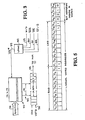
- a video display system designated generally as 1.
- a system bus designated generally as 2.
- a central processing unit CPU
- a system memory coupled to the bus 2 by means of a bus 3
- a DMA controller coupled to the bus 2 by means of a plurality of control buses 10, 11, 12 and 13, there is provided a plurality of graphics controllers designated generally as 14, 15, 16 and 17.
- Controllers 14-17 are also designated 0-n to show that any number of controllers may be cascaded on the bus 2.
- Each of the controllers 14-17 comprise a quad pixel data manager (QPDM) designated generally as 20, a video random access memory (VRAM) designated generally as 21 comprising a plurality of 4 memory planes 21a, 21b, 21c and 21d, and a plurality of video shift registers or 4 video data assembly first-in, first-out memory circuits (VDAF's) designated generally as 22.
- the VRAM 21 is coupled to the QPDM 20 by means of a 64 bit line display memory bus 23.
- the video shift registers or VDAF's 22 are coupled to the VRAM-21 by means of a video data bus 24. Control signals are provided to the video shift registers or VDAF's 22 by the QPDM 20 by means of a control bus 25.
- the outputs of the video shift registers or VDAF's 22 of the controllers 14-17 are coupled to a color look-up table 30 by means of a plurality of signal lines 31, 32, 33 and 34, respectively.
- the output of the color look-up table 30 is coupled to a video monitor 35 comprising a screen 37 by means of a video data bus 36.
- each of the QPDM's 20 in the controllers 14-17 there is provided a sync signal bus 40.
- the sync signal bus 40 is provided for synchronizing all of the QPDM's 20 in the controllers 14-17.
- a graphics microprocessor 50 for executing instructions stored in each of the graphics controllers 14-17 a graphics microprocessor 50, a video refresh circuit 51, a decoder 52, a chip size register 53, a bit map size register 54, an arbiter circuit 55, a memory sequencer circuit 56, and a start bit strobe (SBSTB) generator 57.
- a graphics microprocessor 50 for executing instructions stored in each of the graphics controllers 14-17 a graphics microprocessor 50, a video refresh circuit 51, a decoder 52, a chip size register 53, a bit map size register 54, an arbiter circuit 55, a memory sequencer circuit 56, and a start bit strobe (SBSTB) generator 57.
- SBSTB start bit strobe
- the graphics microprocessor 50 is coupled to the VRAM 21 by means of the display memory bus 23, which for purposes of the present invention is also called a data/mask bus, to the decoder 52 by means of a pair of 12 bit line X and Y logical address buses 60 and 61 and to the arbiter circuit 55 by means of an update request (U REQ ) control signal line 62.
- the video refresh circuit 51 is coupled to the decoder 52 by means of a pair of 12 bit line X and Y logical address buses 63 and 64 and to the arbiter 55 by means of a video request (VREQ) control signal line 65.
- VREQ video request
- the decoder 52 is coupled to the VRAM 21 by means of a 12 bit line RAD/CAD/BANK SELECT physical address bus 70.
- the chip size register 53 is coupled to the decoder 52 by means of a bus 71.
- the bit map size register 54 is coupled to the decoder 52 by means of a signal line 72.
- the arbiter 55 is coupled to the memory sequencer 56 and to the decoder 52 by means of a video acknowledge (V ACK ) control signal line 73 and an update acknowledge (U ACK ) control signal line 74.
- the memory sequencer 56 is coupled to the decoder circuit 52 by means of a row output enable (ROE) control signal line 75 and a column output enable (COE) control signal line 76, to the VRAM 21 and a 16-to-8 multiplexer 77 by means of a pair of video strobe (VSTB) control signal lines 78,79, to the VRAM 21 by means of a write enable (WE) control signal line 80, a row address strobe (RAS) control signal line 81, a column address strobe ( CAS ) control signal line 82 and a transfer/gate enable (XF7G) control signal line 83.
- the lines 81, 82 and 83 are also coupled to corresponding inputs of the SBSTB generator 57.
- the memory sequencer 56 is also coupled to the VDAF's 22 by means of a data strobe (DSTB) control signal line 84, a 3 bit line control data A/B (CDAT A/B) control signal bus 85 and to a full ( FULL ) control signal line 86.
- DSTB data strobe
- CDAT A/B 3 bit line control data A/B
- FULL full
- the SBSTB generator 57 is coupled to the VDAF's 22 by means of a start bit strobe (SBSTB) control signal line 87.
- the multiplexer 77 is coupled to the VDAF's 22 by means of an 8 bit line data bus 88 and to the VRAM 21 by means of a 16 bit line data bus 24.
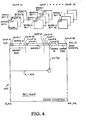
- the VRAM 21 comprises 16 identical memory chips designated chip 0 - chip 15.
- Each of the memory chips 0-15 comprises a 1K x 1K bit memory array 90, a 1K bit data shift register 91, a logical circuit 92.
- the memory array 90 is coupled to the shift register 91 by means of a plurality of 1 K bit lines.
- the output of the shift register 91 is coupled to the multiplexer 77 by means of the multiline bus 24.
- the logic circuit 92 is coupled to the lines 80, 81 and 83 and to one line of the data/mask bus 23.
- each of the chips 0-15 comprises the four identical memory planes designated 21a-21d described above. Planes 21a-21d are provided for storing data corresponding to the primary colors red, blue and green and another pixel attribute such as bright or blinking.
- bit map 100 which corresponds to the VRAM 21 of Fig. 3.
- the bit map 100 is 4K bits wide by 4K bits long. With each word stored in the VRAM 21 comprising 16 bits, each row of the bit map 100 comprises 256 words.
- a bit from each-word in the bit map 100 is stored on a different one of the memory chips 0-15.
- bit 0 of each word is stored on chip 0
- bit 1 of each word is stored on chip 1
- bit 2 of each word is stored on chip 2, etc.
- the address buses 60, 61, 63 and 64 each comprises twelve lines for handling twelve address bits A 0 -A 11 of a pair of X and Y logical or array addresses.
- the VRAM 21 which comprises a plurality of dynamic storage cells
- the translation typically involves the generation of an intermediate linear address which is obtained by adding the X coordinate of the X,Y pair measured in words to the product of the width of the VRAM 21 and the Y coordinate of the X,Y pair measured in words. as follows:
- the linear address is obtained by performing the following mathematical computations:
- fractional remainder in the quotient corresponds to bit number 2 which is the third bit in the desired word. In prior known systems limited to addressing entire words, this fractional remainder would ordinarily be ignored. As will be described below, in accordance with the present invention the fractional remainder may be used for addressing bits within a word when performing a video refresh.
- Equation (3) it will be seen that the first or Y term of the equation (3) is 70 multiplied by a power of 2, namely 8, and that the second or X term of the equation (3) is 50 divided by a power of 2, namely 4.
- multiplying and dividing by powers of 2 is the equivalent of shifting the numbers multiplied and divided by the power of 2, respectively.
- the linear address will appear as shown in Fig. 5.
- the 20 bit linear word address can be multiplexed into a 10 bit RAD and a 10 bit CAD, as shown in Fig. 5, to strobe the address information into the memory chips.
- the address bits X O -X 3 are not used in addressing a word in the bit map 100.
- the address bits X D -X 3 represent specific bits within the word desired. These bits may be retained in an appropriate circuit and used when addressing a specific bit within a desired word.
- 20 X and Y address bits are all that are required to address any location within the memory chip.
- the X and Y address bits X 4 - X 11 and Y 0 -Y 11 may be rearranged and used directly for generating the row physical address (RAD) and the column physical address (CAD) as shown in Fig. 7.
- the address Y 10 and Y 11 are used as a BANK SELECT bits in those embodiments in which the bit map 100 corresponds to a VRAM comprising 512 x 512 bit cells and that Y 8 -Y 11 are used as BANK SELECT bits in those embodiments in which the bit map 100 corresponds to a VRAM comprising 256 x 256 bit memory arrays, respectively.
- the mapping of the address bits in the translation of the logical addresses to the row and column physical addresses RAD and CAD by the decoder 52 as seen in Figs. 7-9 are controlled by the chip size and the bit map size numbers placed in the registers 53 and 54, respectively.
- the updating of the VRAM 21 is initiated by the graphics microprocessor sending an update request (U REQ ) to the arbiter 55.
- the decoder 52 translates the X and Y logical addresses on the buses 60 and 61'into row and column physical addresses RAD and CAD for addressing the VRAM 21 by simply routing the X and Y address bits to their relative positions A 0 -A 11 on the bus 70, as shown in Figs. 7-9 depending on the size of the memory chips and bit map used.
- data on the bus 23 is written into the chips 0-15 at the address identified by the RAD and CAD physical addresses when the transfer signal XF/G is high and the write enable signal WE goes active.
- the signals RAS and CAS strobe RAD and CAD into the chips. If XF/G is low when RAS goes active, a whole row specified by RAD is transferred into the shift register 91. The column position from where the data starts being shifted out is specified by CAD.
- predetermined bits within a word in the bit map 100 are modified. This is accomplished by selectively enabling corresponding ones of the memory chips 0-15 by placing a mask on the data/mask bus 23 and transmitting it to the logic circuit 92.
- a 16-bit mask is placed on the data/mask bus 23 and transferred to the memory chips 0-15, i.e. one mask bit to each chip.
- the bits in the mask corresponding to the bits to be written in the word in the chips 0-15 comprise logical 1's.
- two write enable strobes WE are generated during a write cycle.
- the first is called a mask strobe; the second is called a data strobe.
- the logic circuit 92 in each of the memory chips 0-15 stores the corresponding bit 0-15 in the mask.
- the mask is used for gating the data strobes.
- the data strobe WE will be allowed to propagate through the logic block 92 and will emerge as a gated data write enable signal WE * on the line 95.
- the data strobe signal WE will strobe data on the data bus 23 only into the chip or chips enabled by the mask strobe.
- FIG. 14 there is provided a representation of the bit map 100 on which is superimposed a representation of the screen 37 of the video monitor 35.
- the boundaries of the screen 37 are defined by a logical starting address X S ,Y S and a logical ending address X E ,Y E .
- Within the boundaries of the screen 37 there is represented an apparent window 111.
- the boundaries of the apparent window 111 are defined by an apparent window logical starting address X AS' Y AS and a logical ending address X AE ,Y AE .
- Outside the boundaries..of the screen there is provided a representation of a real window 112.
- the boundaries of the real window 112 are defined by a logical starting address X RS' Y RS and a logical ending address X RE ,Y RE .
- Each row or scan line of the bit map 100 comprises a plurality of 4096-bits, e.g. 256 16-bit words.
- the boundaries of the words are represented by a plurality of vertical lines 113.
- the boundaries of each 8-bit byte in a word are represented by the lines 113 and a plurality of intermediate vertical lines 114.
- the starting and ending addresses of the screen 37, the apparent window 111 and the real window 112 may correspond to bit positions located inside the boundaries of the bit map 110 as well as inside the word and byte boundaries 113 and 114, respectively.
- a video refresh cycle is initiated by the generation of a video request (V REQ ) on the line 65 as shown in Fig. 3.
- V REQ a video request
- the above identified addresses X S ,Y S , X E , Y E , X AS , Y AS , X AE , Y AE , X RS , Y RS , XRE and YRE are transferred by the CPU 4 to the video refresh circuit 51 and the memory sequencer 56.
- transfer cycle signals XF7G, video strobes VSTB and data strobes DSTB are generated by the sequencer 56 and RAD's and CAD's are provided on the bus 70 by the decoder 52 for each of the logical addresses placed on the buses 63,64 by the circuit 51.
- the shift registers 91 are of the addressable type such that the first bit to be shifted out of each register is a bit in a word comprising bits which are to be displayed on the screen 37 as indicated by the address X S .
- word 3 is the first word in the row of data transferred to the shift registers 91 comprising bits to be displayed
- CAD 3 and word 3 is the first word to be shifted out of the registers 91.
- words 4, 5, 6, etc. are shifted out in sequence.
- Words shifted out of the registers 91 are transferred to the VDAF's 22 in 8-bit bytes. Through the 16-to-8 multiplexers 77, however, only those bytes containing bits to be displayed are latched into the VDAF's 22 by the DATA bit strobe DSTB.
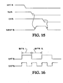
- the start bit strobe SBSTB is generated after the transfer cycle, before the first byte is strobed into the VDAF 22.
- the SBSTB signal is generated together with a signal CDAT A which is placed on the 3-bit lines 85.
- a data strobe DSTB and a CDAT B are generated at the beginning of each byte.
- CDAT B identifies the number of bits in a byte to be displayed.
- CDAT B 8.
- a strobe SBSTB is generated after each transfer cycle and data strobes DSTB are generated for each byte.
- rows having no window segment only one transfer cycle is generated for each row.
- three transfer cycles XF/G are generated for each row; one at the beginning of the screen, one at the beginning of the window segment and another at the end of the window segment.
- a DSTB with a CDAT B 3.
- CDAT A and CDAT B are associated with the first byte of a word if VSTB is HIGH and with the second byte of a word if VSTB is LOW. If the first byte of the word. after a transfer cycle is to be strobed into .-the VDAF, SBSTB and DSTB pulses are generated. If the first byte is to be disregarded, the first DSTB pulse is omitted.
Abstract
Description
- The present invention relates to graphics controllers in general and in particular to a method and apparatus comprising a graphics controller having the capacity for translating X and Y array addresses of words in a bit map into corresponding physical row and column addresses of the words in memory chips without the need for an intermediate linear address, for selectively addressing either 16 bit words or 1 bit words in the bit map and for refreshing a video monitor using bit aligned, as distinguished from word aligned, video screen and window data.
- Video systems comprise graphics controllers and video monitors. In a typical graphics controller there are provided a bit map, a circuit for storing video data in the bit map and a circuit for reading the video data from the bit map onto a video monitor. The operations which take place during the storing of the data in the bit map and the reading of the data from the bit map to the video monitor take place in what are commonly called memory update and video monitor refresh modes, respectively.
- A typical bit map may be thought of as a large array of memory locations comprising a plurality of multi-bit words. For example, a 4K x 4K bit map of 16-bit words comprises a total of over one million words with 256 words in each row of the bit map. The location of each word in the bit map is identified by an X and a Y logical or array address.
- In practice, the bit map actually comprises a plurality of memory chips. For example, a typical memory chip may comprise 1K x 1K storage locations. Therefore, if 1K x 1K memory chips are used, 16 such memory chips are required to store one million 16-bit words. The location of each bit in the memory chip is identified by a row and a column physical address conveniently called RAD and CAD, respectively.
- From the above discussion it is evident that in order to address a bit in a memory chip using the logical address of the word in the bit map, it is necessary to generate a row and a column address of the bit in the memory chip from the logical address of the word in the bit map. This is done by translating the X and Y array or logical address of the word in the bit map into a corresponding row ' and column physical address in the memory chip.
- Heretofore, the apparatus required for translating logical addresses of a word in a bit map to corresponding physical addresses of the bit in a memory chip comprised a graphics controller and a random access memory (RAM) controller. In practice, the RAM controller typically comprised a table look-up memory and an address sequencer.
- In operation, the graphics controller was provided with the X and Y logical addresses of data words in a bit map and the width of the rows as measured in words in the X direction in the memory chips. From this information, the graphics controller generated corresponding linear addresses as follows:
- Linear Address = Y x width + X
- The linear adresses thus generated were then sent to the RAM controller where they were used to generate corresponding row and column physical addresses as well as chip select signals.
- The prior art method of generating row and column physical addresses and chip select signals was costly not only in terms of the time it took to perform the computations, i.e. the product and sums, necessary to generate the linear addresses, but it was also costly in that it required a separate apparatus, i.e. the RAM controller.
- Another disadvantage of the prior art methods and apparatus for addressing a video memory was that no means was provided for addressing individual bits within a word in the bit map. Heretofore, in order to modify one or more individual bits within a word, it was necessary to read the entire word, modify the desired bit(s) and rewrite the word to the memory. As a result, the modification of individual bits within a word, which is often required when modifying lines and curves on a video display, was very time consuming.
- Typically, the number of bits in a bit map in a video system far exceeds the number of pixels on the monitor screen in--the system. As a consequence, when video data is presented on the screen, it is taken from only a portion of the bit map. For example, when writing to the screen there are provided a starting address XS,YS and an ending address XE,YE which correspond to and identify a block of words in the bit map to be displayed on the screen. The data thus identified is then scanned and written to the screen.
- At times, a portion or a section, i.e. window, of a screen of video data is replaced with other data. The replaced window is called an apparent window and is identified by the starting and ending addresses XAS,YAS and XAE,YAE of words in the bit map, respectively.. The replacing window is called a real window and is identified by the starting and ending addresses XRS,YRS and XRE,YRE of words in the bit map, respectively.
- In operation, the data in the bit map to be displayed on the screen is scanned in a regular fashion one line at a time as the physical addresses are generated from the logical addresses. When the address generating apparatus encounters the starting address of an apparent window, it substitutes for the apparent window the data identified by the real addresses XRS'YRS' XRE and YRE.
- Heretofore, the methods and apparatus used for displaying bit map data on a screen and for substituting real window data for apparent window data generally has been restricted to word aligned screens and windows As a consequence, the first and last bit in each uninterrupted portion of a line of data displayed on a screen or in a window has had to correspond to the first and last bit of a word in the bit map. Such a limitation is a significant restriction on the resolution of a video system.
- We will describe a novel method and apparatus comprising means located on a single chip for translating an address of a word in a bit map directly to a corresponding physical address of the word in a memory array without the generation of an intermediate linear or other address.
- We will describe
means responsive to a mask and a control signal for modifying any group of bits identified in a word. - Wewill also describe
method and apparatus comprising a video memory and means for. displaying video data on a monitor screen and/or in a window on the screen wherein the first and/or last bit of the displayed data on the screen and/or in the window on the screen may correspond to any bit in a word in the video memory. - There is provided a decoder, a chip size register, a bit map size register, an array address input bus, a physical address output bus, and a data/mask bus.
- The array address input bus is provided for sending an X and Y array address of a word in a bit map from a graphics microprocessor to the decoder. The physical address output bus is provided for sending a row and column physical address of the word from the decoder to "memory chips. The chip size register and the bit map size register are provided for controlling the translation of the array address to a corresponding physical address in the decoder. The data/mask bus is provided for sending data and mask information to the memory chips.
- For purposes of describing the translation of array addresses to physical addresses,
there is provided a rectangular bit map comprising 4K x 4K rows and columns of 16-bit words with -256 words in each row. Corresponding to the bit map there are provided 16 1K x 1K memory chips. The memory chips are organized in such a manner that each of the memory chips stores one bit from each of the 16-bit words in the bit map. For example, bit 0 of all of the words in the bit map is stored on chip 0,bit 1 of all of the words is stored onchip 1,bit 2 of all of the words is stored onchip 2, etc. As a consequence, whenever a word is addressed, all 16 memory chips are automatically selected simultaneously thus eliminating the need to generate a specific chip select signal. - Each array address comprises 24 bits, e.g. X0-X11 and Y0-Y11. Four bits of the 24-bit X and Y array address, e.g. X0-X3, are available to be used for generating a mask. The remaining 20 bits, e.g. X4-X11 and Y0-Y11 are sufficient to address the 1K x 1K memory chips.
- The use of the array address bits X4-X11 and Y0-Y11 in the decoder to generate the row and column physical addresses RAD and CAD depends on the bit map size and the chip size. For example, with a 4K x 4K bit map and 16 1K x 1K memory chips, array address bits Y0-Y9 are used directly as the physical row address RAD and array address bits X4-X11, Y10 and Y11 are used directly as the physical column address CAD. With a 4K x 4K bit map and 16 512 x 512 memory chips in each of four banks, array address bits Y0-Y8 are used directly as the physical row address RAD, array address bits X4-X11 and Y9 are used directly as the physical column address CAD and array address bits Y10 and Y11 are used directly to select one of the four banks. With a 4K x 4K bit map and 16 256 x 256 memory chips in each of 16 banks, array address bits Y0-Y7 are used directly as the physical row address RAD, array address bits X4-X11 are used directly as the physical column address CAD and array address bits Y8-Y11 are used directly to select one of the 16 banks.
- When updating the bit map, it is often desirable to change one or more pixels in a word without disturbing the remaining pixels in the word. Accordingly, there is further provided in accordance with the above objects means responsive to a control signal designated WE and the above described mask for modifying any selected group of bits inside a word. For example, in one embodiment, the bits Xp-X3 are used to generate the mask and identify one of the 16 bits of a word addressed by the remaining address bits X4-X11 and Y0-Y11. In this manner, the identified bit can be changed in the addressed word.
- Further in accordance.
there are provided a video data assembly first-in, first-out memory circuit (VDAF) and associated control signal generators. The VDAF is provided for allowing.the display of bit aligned, as distinguished from word aligned, data on a video monitor. For example, when a full screen of data is to be written to the monitor, the starting and ending addresses of the corresponding data in the bit map are examined. If the examined addresses indicate that the data to be displayed is not word aligned, e.g. the left edge of the displayed data corresponds to the third bit in each of the data words involved, the data words are transferred out of the bit map but only the bits to be displayed are transmitted out of the VDAF to the screen. The method and apparatus used for displaying a screen of bit aligned data are also used for displaying bit aligned windows of data, i.e. blocks of data which comprise less than a full screen. - The above and other features and advantages of the present invention will become apparent from the following description of the accompanying drawing in which:
- Fig. 1 is a block diagram of a video system according to the present invention;
- Fig. 2 is a detailed block diagram of an embodiment of the present invention;
- Fig. 3 is a block diagram of a plurality of memory arrays according to the present invention;
- Fig. 4 is a diagram of a bit map and a plurality of memory arrays according to the present invention;
- Fig. 5 is a diagram of a RAD and CAD address according to the present invention wherein Y10 and Y11 are used as the two most significant bits of the CAD for addressing 1K x 1K memory arrays;
- Fig. 6 is a diagram of an exemplary X and Y address prior to translation according to the present invention;
- Figs. 7-9 are diagrams of the translation of three logical addresses into three physical addresses according to the present invention;
- Fig. 10 is a block diagram showing a data register and array of memory chips according to the present invention;
- Fig. 11 is a plurality of timing diagrams showing the relationship of timing signals for normal read/write update and video refresh operations;
- Fig. 12 is a block diagram of a data/mask register and a plurality of memory arrays according to the present invention; and
- Fig. 13 is a plurality of timing diagrams showing the relationship of timing signals during a masked write operation.
- Fig. 14 is a detailed diagram of a bit map showing the control signals used for transferring data from a plurality of memory arrays for display on a video monitor according to the present invention;
- Fig. 15 is a plurality of timing diagrams showing the generation of a start bit strobe control signal according to the present invention;
- Fig. 16 is a timing diagram showing the relationship between-a video strobe and a data strobe according to the present invention;
- Referring to Fig. 1, there is provided in accordance with the present invention a video display system designated generally as 1. In the
display system 1 there is provided a system bus designated generally as 2. Coupled to thebus 2 by means of abus 3 there is provided a central processing unit (CPU) 4. Coupled to thebus 2 by means of abus 5 there is provided asystem memory 6. Coupled to thebus 2 by means of a bus 7 there is provided aDMA controller 8. Also coupled to thebus 2 by means of a plurality ofcontrol buses bus 2. - Each of the controllers 14-17 comprise a quad pixel data manager (QPDM) designated generally as 20, a video random access memory (VRAM) designated generally as 21 comprising a plurality of 4
memory planes 21a, 21b, 21c and 21d, and a plurality of video shift registers or 4 video data assembly first-in, first-out memory circuits (VDAF's) designated generally as 22. TheVRAM 21 is coupled to theQPDM 20 by means of a 64 bit linedisplay memory bus 23. The video shift registers or VDAF's 22 are coupled to the VRAM-21 by means of avideo data bus 24. Control signals are provided to the video shift registers or VDAF's 22 by theQPDM 20 by means of acontrol bus 25. The outputs of the video shift registers or VDAF's 22 of the controllers 14-17 are coupled to a color look-up table 30 by means of a plurality ofsignal lines video monitor 35 comprising ascreen 37 by means of a video data bus 36. Coupling. each of the QPDM's 20 in the controllers 14-17 there is provided async signal bus 40. Thesync signal bus 40 is provided for synchronizing all of the QPDM's 20 in the controllers 14-17. - Referring to Fig. 2, there is provided in each of the graphics controllers 14-17 a
graphics microprocessor 50, avideo refresh circuit 51, a decoder 52, a chip size register 53, a bitmap size register 54, anarbiter circuit 55, amemory sequencer circuit 56, and a start bit strobe (SBSTB)generator 57. - The
graphics microprocessor 50 is coupled to theVRAM 21 by means of thedisplay memory bus 23, which for purposes of the present invention is also called a data/mask bus, to the decoder 52 by means of a pair of 12 bit line X and Ylogical address buses arbiter circuit 55 by means of an update request (UREQ)control signal line 62. - The
video refresh circuit 51 is coupled to the decoder 52 by means of a pair of 12 bit line X and Ylogical address buses arbiter 55 by means of a video request (VREQ)control signal line 65. - The decoder 52 is coupled to the
VRAM 21 by means of a 12 bit line RAD/CAD/BANK SELECTphysical address bus 70. The chip size register 53 is coupled to the decoder 52 by means of a bus 71. The bitmap size register 54 is coupled to the decoder 52 by means of asignal line 72. Thearbiter 55 is coupled to thememory sequencer 56 and to the decoder 52 by means of a video acknowledge (VACK)control signal line 73 and an update acknowledge (UACK)control signal line 74. - The
memory sequencer 56 is coupled to the decoder circuit 52 by means of a row output enable (ROE)control signal line 75 and a column output enable (COE) control signal line 76, to theVRAM 21 and a 16-to-8multiplexer 77 by means of a pair of video strobe (VSTB)control signal lines VRAM 21 by means of a write enable (WE)control signal line 80, a row address strobe (RAS)control signal line 81, a column address strobe (CAS )control signal line 82 and a transfer/gate enable (XF7G)control signal line 83. Thelines SBSTB generator 57. - The
memory sequencer 56 is also coupled to the VDAF's 22 by means of a data strobe (DSTB)control signal line 84, a 3 bit line control data A/B (CDAT A/B) control signal bus 85 and to a full (FULL )control signal line 86. - The
SBSTB generator 57 is coupled to the VDAF's 22 by means of a start bit strobe (SBSTB)control signal line 87. Themultiplexer 77 is coupled to the VDAF's 22 by means of an 8 bitline data bus 88 and to theVRAM 21 by means of a 16 bitline data bus 24. - Referring to Fig. 3, in one embodiment of the present invention, the
VRAM 21 comprises 16 identical memory chips designated chip 0 -chip 15. Each of the memory chips 0-15 comprises a 1K x 1Kbit memory array 90, a 1K bit data shiftregister 91, alogical circuit 92. Thememory array 90 is coupled to theshift register 91 by means of a plurality of 1K bit lines. The output of theshift register 91 is coupled to themultiplexer 77 by means of themultiline bus 24. Thelogic circuit 92 is coupled to thelines mask bus 23. - In addition to the above, each of the chips 0-15 comprises the four identical memory planes designated 21a-21d described above.
Planes 21a-21d are provided for storing data corresponding to the primary colors red, blue and green and another pixel attribute such as bright or blinking. - Referring to Fig. 4, there is provided a bit map designated generally as 100 which corresponds to the
VRAM 21 of Fig. 3. Thebit map 100 is 4K bits wide by 4K bits long. With each word stored in theVRAM 21 comprising 16 bits, each row of thebit map 100 comprises 256 words. The total number of the words represented by the bit map_comprises 1,048,576. - In accordance with the present invention, a bit from each-word in the
bit map 100 is stored on a different one of the memory chips 0-15. For example, bit 0 of each word is stored on chip 0,bit 1 of each word is stored onchip 1,bit 2 of each word is stored onchip 2, etc. Thus when addressing a word in thebit map 100 in the execution of a normal read/write operation, all of the memory chips 0-15 are selected simultaneously and automatically. Therefore, it is not necessary to generate a separate address on theaddress buses bit map 100. - The
address buses - As is well known, to address one of the chips 0-15 in the
VRAM 21 which comprises a plurality of dynamic storage cells, it is necessary to translate the logical address pair X,Y to a pair of physical addresses. The translation typically involves the generation of an intermediate linear address which is obtained by adding the X coordinate of the X,Y pair measured in words to the product of the width of theVRAM 21 and the Y coordinate of the X,Y pair measured in words. as follows:
- For example, if the logical or array address of a word in the
bit map 100 has the coordinates Y=70 and X=50 as shown in Fig. 4, the linear address is obtained by performing the following mathematical computations:
- 4096 = number of bits in a row or scanline of the
bit map 100 - 16 = number of bits in a word in the
bit map 100 - 70 = number of entire rows preceding the row in which the desired word is located
- 50 = the bit position in a row of a bit in the desired word
- *The fractional remainder in the quotient corresponds to bit
number 2 which is the third bit in the desired word. In prior known systems limited to addressing entire words, this fractional remainder would ordinarily be ignored. As will be described below, in accordance with the present invention the fractional remainder may be used for addressing bits within a word when performing a video refresh. - In accordance with the present invention, it was also recognized that so long as a bit map corresponds to a memory array having a width as measured in words equal in number to a power of 2 and words comprise bits equal in number to a power of. 2, the time consuming divisions, multiplications and additions in the above-described computations for a linear address could be reduced to simple left and right shift operations in general, and more specifically, they could be performed in a simple combinatorial circuit. For example, equation (1) above can be written as follows:


- Referring to Figs. 5 and 6, concatenating the X and Y logical addresses one obtains 24 address bits. Referring to equation (3), it will be seen that the first or Y term of the equation (3) is 70 multiplied by a power of 2, namely 8, and that the second or X term of the equation (3) is 50 divided by a power of 2, namely 4. As previously mentioned, multiplying and dividing by powers of 2 is the equivalent of shifting the numbers multiplied and divided by the power of 2, respectively. Thus, if one shifts the binary equivalent of 70 eight places to the left and the binary equivalent of 50 four places to the right and concatenates them, the linear address will appear as shown in Fig. 5. In the case when the bit map is implemented with 1K x 1K memory chips, the 20 bit linear word address can be multiplexed into a 10 bit RAD and a 10 bit CAD, as shown in Fig. 5, to strobe the address information into the memory chips.
- It will be noted from the above operations that by shifting the X term to the right four places, the address bits XO-X3 are not used in addressing a word in the
bit map 100. However, it will be noted that the address bits XD-X3 represent specific bits within the word desired. These bits may be retained in an appropriate circuit and used when addressing a specific bit within a desired word. It will also be noted that since each of the chips 0-15 comprise 1K x 1K memory cells, 20 X and Y address bits are all that are required to address any location within the memory chip. As a consequence, the X and Y address bits X 4-X 11 and Y0-Y11 may be rearranged and used directly for generating the row physical address (RAD) and the column physical address (CAD) as shown in Fig. 7. - Referring to Figs. 8 and 9, it will be noted that the address Y10 and Y11 are used as a BANK SELECT bits in those embodiments in which the
bit map 100 corresponds to a VRAM comprising 512 x 512 bit cells and that Y8-Y11 are used as BANK SELECT bits in those embodiments in which thebit map 100 corresponds to a VRAM comprising 256 x 256 bit memory arrays, respectively. The mapping of the address bits in the translation of the logical addresses to the row and column physical addresses RAD and CAD by the decoder 52 as seen in Figs. 7-9 are controlled by the chip size and the bit map size numbers placed in theregisters 53 and 54, respectively. - In operation, the updating of the
VRAM 21 is initiated by the graphics microprocessor sending an update request (UREQ) to thearbiter 55. In response to the update request, if no video request which takes priority is present, the decoder 52 translates the X and Y logical addresses on thebuses 60 and 61'into row and column physical addresses RAD and CAD for addressing theVRAM 21 by simply routing the X and Y address bits to their relative positions A0-A11 on thebus 70, as shown in Figs. 7-9 depending on the size of the memory chips and bit map used. - Referring to Figs. 10 and 11, data on the
bus 23 is written into the chips 0-15 at the address identified by the RAD and CAD physical addresses when the transfer signalXF/G is high and the write enable signal WE goes active. The signals RAS and CAS strobe RAD and CAD into the chips. IfXF/G is low whenRAS goes active, a whole row specified by RAD is transferred into theshift register 91. The column position from where the data starts being shifted out is specified by CAD. - To make modifications to lines and curves displayed on the
video monitor 35, predetermined bits within a word in thebit map 100 are modified. This is accomplished by selectively enabling corresponding ones of the memory chips 0-15 by placing a mask on the data/mask bus 23 and transmitting it to thelogic circuit 92. - Referring to Figs. 2, 3, 12 and 13, in operation when a selected bit in a word is to be written, a 16-bit mask is placed on the data/
mask bus 23 and transferred to the memory chips 0-15, i.e. one mask bit to each chip. The bits in the mask corresponding to the bits to be written in the word in the chips 0-15 comprise logical 1's. - When the mask is used, two write enable strobes
WE are generated during a write cycle. The first is called a mask strobe; the second is called a data strobe. If RAS goes LOW when the mask strobe is LOW, thelogic circuit 92 in each of the memory chips 0-15 stores the corresponding bit 0-15 in the mask. The mask is used for gating the data strobes. In the case where the bit in the stored mask is a logical 1, the data strobe WE will be allowed to propagate through thelogic block 92 and will emerge as a gated data write enable signalWE * on theline 95. Thus, the data strobe signal WE will strobe data on thedata bus 23 only into the chip or chips enabled by the mask strobe. For example, if only bit 5 of a word is to be written, onlychip 5 will be enabled by the mask whenWE * is generated. Alternatively, ifonly bits - Referring to Fig. 14, there is provided a representation of the
bit map 100 on which is superimposed a representation of thescreen 37 of thevideo monitor 35. The boundaries of thescreen 37 are defined by a logical starting address XS,YS and a logical ending address XE,YE. Within the boundaries of thescreen 37 there is represented an apparent window 111. The boundaries of the apparent window 111 are defined by an apparent window logical starting address XAS'YAS and a logical ending address XAE,YAE. Outside the boundaries..of the screen there is provided a representation of a real window 112. The boundaries of the real window 112 are defined by a logical starting address XRS'YRS and a logical ending address XRE,YRE. - Each row or scan line of the
bit map 100 comprises a plurality of 4096-bits, e.g. 256 16-bit words. The boundaries of the words are represented by a plurality ofvertical lines 113. The boundaries of each 8-bit byte in a word are represented by thelines 113 and a plurality of intermediatevertical lines 114. - As shown in Fig. 14, the starting and ending addresses of the
screen 37, the apparent window 111 and the real window 112 may correspond to bit positions located inside the boundaries of the bit map 110 as well as inside the word andbyte boundaries - In operation, a video refresh cycle is initiated by the generation of a video request (VREQ) on the
line 65 as shown in Fig. 3. Prior to the video refresh operation, the above identified addresses XS,YS, XE, YE, XAS, YAS, XAE, YAE, XRS, YRS, XRE and YRE are transferred by theCPU 4 to thevideo refresh circuit 51 and thememory sequencer 56. In response to these addresses, transfer cycle signals XF7G, video strobes VSTB and data strobes DSTB are generated by thesequencer 56 and RAD's and CAD's are provided on thebus 70 by the decoder 52 for each of the logical addresses placed on thebuses circuit 51. - In response to the transfer cycle signal
XF/G , and a RAD, an entire row of data addressed by the RAD in each of the memory chips 0-15 is transferred in parallel to theshift register 91 associated with that memory chip. Thereafter, in response to each VSTB, a bit is shifted out of each ofregisters 91 such that a 16-bit word is made available to the VDAF's 22 with each VSTB. - At this point it should be noted that the shift registers 91 are of the addressable type such that the first bit to be shifted out of each register is a bit in a word comprising bits which are to be displayed on the
screen 37 as indicated by the address XS. For example, if, as shown in Fig. 4,word 3 is the first word in the row of data transferred to the shift registers 91 comprising bits to be displayed, then CAD = 3 andword 3 is the first word to be shifted out of theregisters 91. Afterword 3 is shifted out of theregisters 91,words - Even though
word 3 is shifted out of the shift registers 91, not all of the bits of the word will necessarily be latched into the VDAF's 22. Words shifted out of theregisters 91 are transferred to the VDAF's 22 in 8-bit bytes. Through the 16-to-8multiplexers 77, however, only those bytes containing bits to be displayed are latched into the VDAF's 22 by the DATA bit strobe DSTB. - The start bit strobe SBSTB, is generated after the transfer cycle, before the first byte is strobed into the
VDAF 22. The SBSTB signal is generated together with a signal CDAT A which is placed on the 3-bit lines 85. CDAT A identifies the first bit to be displayed and consequently the first bit to be shifted out of the VDAF's 22 to the color look-up table 30. In the example shown in Fig. 14, CDAT A = 5 as determined by the starting address X . - Following the generation of the strobe SBSTB and CDAT A, a data strobe DSTB and a CDAT B are generated at the beginning of each byte. CDAT B identifies the number of bits in a byte to be displayed. In the present example, in the row defined as YS, the first DSTB signal is accompanied by CDAT B = 3, indicating that the first byte has three bits to be displayed. Then, three complete bytes are described by CDAT B = 8. At the right end of the row YS defined by XE, CDAT B = 6 is generated. This means that only 'six bits in
byte 2 ofword 3 are to be displayed. - At the end of row YS defined by XE, Y is incremented to Ys+1, another transfer cycle
XF/G is generated and the above described operations are repeated. These.operations are repeated for each row displayed on the screen until a row with a window is encountered. - Referring to Figs. 15 and 16, a strobe SBSTB is generated after each transfer cycle and data strobes DSTB are generated for each byte. In rows having no window segment, only one transfer cycle is generated for each row. In rows having a window segment, three transfer cycles
XF/G are generated for each row; one at the beginning of the screen, one at the beginning of the window segment and another at the end of the window segment. For example, in a row containing a window segment such as the row defined by YAS in Fig. 14, the first SBSTB with a CDAT A = 5 is generated. This is followed by a DSTB with a CDAT B = 3. Another DSTB with a CDAT B = 6 follows. CDAT B = 3 indicates that 3 bits ofbyte 2 ofword 1 are to be displayed. CDAT B = 6 indicates that 6 bits ofbyte 1 ofword 2 are to be displayed. Next, the second transfer cycle with SBSTB with a CDAT A = 0 is generated to define the start of the real window. The CDAT A = 0 indicates that the starting bit is the first bit of the byte. This SBSTB is followed by two DSTB's with a CDAT B = 8 and one DSTB with a CDAT B = 3. After the last DSTB, the third transfer cycle with SBSTB is generated with a CDAT A = 1. The latter CDAT A = 1 indicates that the remaining background to be displayed on the screen begins withbit 1 ofbyte 2 ofword 3. This is followed by DSTB with CDAT B = 5. As seen in Fig. 16, CDAT A and CDAT B are associated with the first byte of a word if VSTB is HIGH and with the second byte of a word if VSTB is LOW. If the first byte of the word. after a transfer cycle is to be strobed into .-the VDAF, SBSTB and DSTB pulses are generated. If the first byte is to be disregarded, the first DSTB pulse is omitted. - While a preferred embodiment of the present invention is described above, it is understood that various modifications may be made thereto without departing from the spirit and scope thereof. Accordingly, it is intended that the scope of the invention not be limited to the embodiments described but be determined by reference to the claims hereinafter provided.
Claims (26)
Applications Claiming Priority (2)
| Application Number | Priority Date | Filing Date | Title |
|---|---|---|---|
| US06/853,586 US4912658A (en) | 1986-04-18 | 1986-04-18 | Method and apparatus for addressing video RAMS and refreshing a video monitor with a variable resolution |
| US853586 | 1986-04-18 |
Publications (2)
| Publication Number | Publication Date |
|---|---|
| EP0244112A2 true EP0244112A2 (en) | 1987-11-04 |
| EP0244112A3 EP0244112A3 (en) | 1990-08-22 |
Family
ID=25316432
Family Applications (1)
| Application Number | Title | Priority Date | Filing Date |
|---|---|---|---|
| EP87303151A Withdrawn EP0244112A3 (en) | 1986-04-18 | 1987-04-10 | A method and apparatus for addressing video rams and refreshing a video monitor with a variable resolution |
Country Status (3)
| Country | Link |
|---|---|
| US (1) | US4912658A (en) |
| EP (1) | EP0244112A3 (en) |
| JP (1) | JPS62251977A (en) |
Cited By (2)
| Publication number | Priority date | Publication date | Assignee | Title |
|---|---|---|---|---|
| EP0338416A2 (en) * | 1988-04-20 | 1989-10-25 | International Business Machines Corporation | Virtual display adapter |
| EP0358353A2 (en) * | 1988-09-06 | 1990-03-14 | International Business Machines Corporation | Data transfers between memories |
Families Citing this family (11)
| Publication number | Priority date | Publication date | Assignee | Title |
|---|---|---|---|---|
| US4992956A (en) * | 1987-10-08 | 1991-02-12 | Advanced Micro Devices, Inc. | Apparatus for assembling data for supply to a scanning output device |
| US4991110A (en) * | 1988-09-13 | 1991-02-05 | Silicon Graphics, Inc. | Graphics processor with staggered memory timing |
| US5047958A (en) * | 1989-06-15 | 1991-09-10 | Digital Equipment Corporation | Linear address conversion |
| US5329617A (en) * | 1989-07-23 | 1994-07-12 | Texas Instruments Incorporated | Graphics processor nonconfined address calculation system |
| JPH05225045A (en) * | 1992-02-17 | 1993-09-03 | Canon Inc | Sequence controller |
| WO1994029871A1 (en) * | 1993-06-14 | 1994-12-22 | Rambus, Inc. | Method and apparatus for writing to memory components |
| KR0179166B1 (en) * | 1995-10-04 | 1999-05-01 | 문정환 | Memory device for digital image signal processing |
| US5841446A (en) * | 1996-11-01 | 1998-11-24 | Compaq Computer Corp. | Method and apparatus for address mapping of a video memory using tiling |
| US6032243A (en) * | 1997-04-01 | 2000-02-29 | United Microelectronics Corp. | Data-transfer interconnection for signal and data transfer between CD-ROM decoder and buffer memory |
| US20100204979A1 (en) * | 2009-02-06 | 2010-08-12 | Inventec Corporation | System and method for magnifiedly displaying real-time translated word |
| CN109388358B (en) * | 2017-08-03 | 2021-12-17 | 富泰华工业(深圳)有限公司 | Electronic equipment and video frame arrangement method |
Citations (5)
| Publication number | Priority date | Publication date | Assignee | Title |
|---|---|---|---|---|
| US4236228A (en) * | 1977-03-17 | 1980-11-25 | Tokyo Shibaura Electric Co., Ltd. | Memory device for processing picture images data |
| GB2128004A (en) * | 1982-08-27 | 1984-04-18 | Nec Corp | Display radio paging receiver for variable length messages |
| EP0106121A2 (en) * | 1982-09-20 | 1984-04-25 | Kabushiki Kaisha Toshiba | Video RAM write control apparatus |
| EP0130340A2 (en) * | 1983-06-30 | 1985-01-09 | International Business Machines Corporation | Memory mapping and readout system |
| EP0166620A2 (en) * | 1984-06-27 | 1986-01-02 | Tektronix, Inc. | Graphics display apparatus |
Family Cites Families (18)
| Publication number | Priority date | Publication date | Assignee | Title |
|---|---|---|---|---|
| US4564915A (en) * | 1980-04-11 | 1986-01-14 | Ampex Corporation | YIQ Computer graphics system |
| JPS588348A (en) * | 1981-07-07 | 1983-01-18 | Sony Corp | Microcomputer |
| JPS5836089A (en) * | 1981-08-27 | 1983-03-02 | Sony Corp | Picture display device |
| US4667305A (en) * | 1982-06-30 | 1987-05-19 | International Business Machines Corporation | Circuits for accessing a variable width data bus with a variable width data field |
| US4691295A (en) * | 1983-02-28 | 1987-09-01 | Data General Corporation | System for storing and retreiving display information in a plurality of memory planes |
| JPS59180871A (en) * | 1983-03-31 | 1984-10-15 | Fujitsu Ltd | Semiconductor memory device |
| US4646262A (en) * | 1983-07-20 | 1987-02-24 | Ramtek Corporation | Feedback vector generator for storage of data at a selectable rate |
| US4580135A (en) * | 1983-08-12 | 1986-04-01 | International Business Machines Corporation | Raster scan display system |
| GB8322438D0 (en) * | 1983-08-19 | 1983-10-12 | Marconi Avionics | Display systems |
| US4620186A (en) * | 1983-08-30 | 1986-10-28 | Zenith Electronics Corporation | Multi-bit write feature for video RAM |
| JPS6067989A (en) * | 1983-09-26 | 1985-04-18 | 株式会社日立製作所 | Image display circuit |
| CA1231186A (en) * | 1983-12-20 | 1988-01-05 | Takatoshi Ishii | Display control system |
| CA1243138A (en) * | 1984-03-09 | 1988-10-11 | Masahiro Kodama | High speed memory access circuit of crt display unit |
| US4663729A (en) * | 1984-06-01 | 1987-05-05 | International Business Machines Corp. | Display architecture having variable data width |
| US4663619A (en) * | 1985-04-08 | 1987-05-05 | Honeywell Inc. | Memory access modes for a video display generator |
| SE454224B (en) * | 1985-04-10 | 1988-04-11 | Lundstrom Jan Erik | SCREEN UNIT FOR PRESENTATION OF GRAPHIC INFORMATION |
| US4745407A (en) * | 1985-10-30 | 1988-05-17 | Sun Microsystems, Inc. | Memory organization apparatus and method |
| US4773044A (en) * | 1986-11-21 | 1988-09-20 | Advanced Micro Devices, Inc | Array-word-organized display memory and address generator with time-multiplexed address bus |
-
1986
- 1986-04-18 US US06/853,586 patent/US4912658A/en not_active Expired - Lifetime
-
1987
- 1987-04-10 EP EP87303151A patent/EP0244112A3/en not_active Withdrawn
- 1987-04-16 JP JP62094249A patent/JPS62251977A/en active Pending
Patent Citations (5)
| Publication number | Priority date | Publication date | Assignee | Title |
|---|---|---|---|---|
| US4236228A (en) * | 1977-03-17 | 1980-11-25 | Tokyo Shibaura Electric Co., Ltd. | Memory device for processing picture images data |
| GB2128004A (en) * | 1982-08-27 | 1984-04-18 | Nec Corp | Display radio paging receiver for variable length messages |
| EP0106121A2 (en) * | 1982-09-20 | 1984-04-25 | Kabushiki Kaisha Toshiba | Video RAM write control apparatus |
| EP0130340A2 (en) * | 1983-06-30 | 1985-01-09 | International Business Machines Corporation | Memory mapping and readout system |
| EP0166620A2 (en) * | 1984-06-27 | 1986-01-02 | Tektronix, Inc. | Graphics display apparatus |
Cited By (4)
| Publication number | Priority date | Publication date | Assignee | Title |
|---|---|---|---|---|
| EP0338416A2 (en) * | 1988-04-20 | 1989-10-25 | International Business Machines Corporation | Virtual display adapter |
| EP0338416A3 (en) * | 1988-04-20 | 1991-12-11 | International Business Machines Corporation | Virtual display adapter |
| EP0358353A2 (en) * | 1988-09-06 | 1990-03-14 | International Business Machines Corporation | Data transfers between memories |
| EP0358353A3 (en) * | 1988-09-06 | 1991-08-21 | International Business Machines Corporation | Data transfers between memories |
Also Published As
| Publication number | Publication date |
|---|---|
| JPS62251977A (en) | 1987-11-02 |
| US4912658A (en) | 1990-03-27 |
| EP0244112A3 (en) | 1990-08-22 |
Similar Documents
| Publication | Publication Date | Title |
|---|---|---|
| US4742344A (en) | Digital display system with refresh memory for storing character and field attribute data | |
| US4745407A (en) | Memory organization apparatus and method | |
| EP0197412B1 (en) | Variable access frame buffer memory | |
| US5680161A (en) | Method and apparatus for high speed graphics data compression | |
| US5129059A (en) | Graphics processor with staggered memory timing | |
| EP0197413B1 (en) | Frame buffer memory | |
| EP0012420A1 (en) | Methods of operating display devices and apparatus for performing the methods | |
| EP0279693B1 (en) | Multi-plane video ram | |
| US4912658A (en) | Method and apparatus for addressing video RAMS and refreshing a video monitor with a variable resolution | |
| US4876663A (en) | Display interface system using buffered VDRAMs and plural shift registers for data rate control between data source and display | |
| US4673930A (en) | Improved memory control for a scanning CRT visual display system | |
| EP0778577B1 (en) | A Synchronous semiconductor memory integrated circuit, a method for accessing said memory and a system comprising such a memory | |
| EP0215984B1 (en) | Graphic display apparatus with combined bit buffer and character graphics store | |
| JPH052154B2 (en) | ||
| EP0145320A2 (en) | Method for multiplexing a memory data bus | |
| GB2214038A (en) | Image display system | |
| US5642138A (en) | Display control system using a different clock in the graphics mode from that in the text mode in accessing an image memory | |
| US5119331A (en) | Segmented flash write | |
| US5699498A (en) | Technique and apparatus for color expansion into a non-aligned 24 bit RGB color-space format | |
| KR960700481A (en) | MULTIPLE BLOCK MODE OPERATIONS IN A FRAME BUFFER SYSTEM DESIGNED FOR WINDOWING OPERATIONS Designed for Windowing Operation | |
| EP0283579B1 (en) | Raster scan display system with random access memory character generator | |
| US4956640A (en) | Method and apparatus for controlling video display priority | |
| JP3002951B2 (en) | Image data storage controller | |
| JPH0340072A (en) | Memory device having address control function | |
| JPS6326896A (en) | Semiconductor memory |
Legal Events
| Date | Code | Title | Description |
|---|---|---|---|
| PUAI | Public reference made under article 153(3) epc to a published international application that has entered the european phase |
Free format text: ORIGINAL CODE: 0009012 |
|
| AK | Designated contracting states |
Kind code of ref document: A2 Designated state(s): AT BE CH DE ES FR GB GR IT LI LU NL SE |
|
| PUAL | Search report despatched |
Free format text: ORIGINAL CODE: 0009013 |
|
| AK | Designated contracting states |
Kind code of ref document: A3 Designated state(s): AT BE CH DE ES FR GB GR IT LI LU NL SE |
|
| 17P | Request for examination filed |
Effective date: 19901122 |
|
| 17Q | First examination report despatched |
Effective date: 19920721 |
|
| STAA | Information on the status of an ep patent application or granted ep patent |
Free format text: STATUS: THE APPLICATION IS DEEMED TO BE WITHDRAWN |
|
| 18D | Application deemed to be withdrawn |
Effective date: 19940401 |
|
| RIN1 | Information on inventor provided before grant (corrected) |
Inventor name: SFARTI, ADRIAN Inventor name: STRUPAT, ACHIM |