EP0247603A2 - A method for stripping a photo resist on an aluminium alloy - Google Patents
A method for stripping a photo resist on an aluminium alloy Download PDFInfo
- Publication number
- EP0247603A2 EP0247603A2 EP87107743A EP87107743A EP0247603A2 EP 0247603 A2 EP0247603 A2 EP 0247603A2 EP 87107743 A EP87107743 A EP 87107743A EP 87107743 A EP87107743 A EP 87107743A EP 0247603 A2 EP0247603 A2 EP 0247603A2
- Authority
- EP
- European Patent Office
- Prior art keywords
- gas
- substrate
- aluminum alloy
- etching
- stripping
- Prior art date
- Legal status (The legal status is an assumption and is not a legal conclusion. Google has not performed a legal analysis and makes no representation as to the accuracy of the status listed.)
- Granted
Links
Images
Classifications
-
- H—ELECTRICITY
- H01—ELECTRIC ELEMENTS
- H01L—SEMICONDUCTOR DEVICES NOT COVERED BY CLASS H10
- H01L21/00—Processes or apparatus adapted for the manufacture or treatment of semiconductor or solid state devices or of parts thereof
- H01L21/02—Manufacture or treatment of semiconductor devices or of parts thereof
- H01L21/04—Manufacture or treatment of semiconductor devices or of parts thereof the devices having at least one potential-jump barrier or surface barrier, e.g. PN junction, depletion layer or carrier concentration layer
- H01L21/18—Manufacture or treatment of semiconductor devices or of parts thereof the devices having at least one potential-jump barrier or surface barrier, e.g. PN junction, depletion layer or carrier concentration layer the devices having semiconductor bodies comprising elements of Group IV of the Periodic System or AIIIBV compounds with or without impurities, e.g. doping materials
- H01L21/30—Treatment of semiconductor bodies using processes or apparatus not provided for in groups H01L21/20 - H01L21/26
- H01L21/302—Treatment of semiconductor bodies using processes or apparatus not provided for in groups H01L21/20 - H01L21/26 to change their surface-physical characteristics or shape, e.g. etching, polishing, cutting
-
- H—ELECTRICITY
- H01—ELECTRIC ELEMENTS
- H01L—SEMICONDUCTOR DEVICES NOT COVERED BY CLASS H10
- H01L21/00—Processes or apparatus adapted for the manufacture or treatment of semiconductor or solid state devices or of parts thereof
- H01L21/02—Manufacture or treatment of semiconductor devices or of parts thereof
- H01L21/02041—Cleaning
- H01L21/02057—Cleaning during device manufacture
- H01L21/02068—Cleaning during device manufacture during, before or after processing of conductive layers, e.g. polysilicon or amorphous silicon layers
- H01L21/02071—Cleaning during device manufacture during, before or after processing of conductive layers, e.g. polysilicon or amorphous silicon layers the processing being a delineation, e.g. RIE, of conductive layers
-
- G—PHYSICS
- G03—PHOTOGRAPHY; CINEMATOGRAPHY; ANALOGOUS TECHNIQUES USING WAVES OTHER THAN OPTICAL WAVES; ELECTROGRAPHY; HOLOGRAPHY
- G03F—PHOTOMECHANICAL PRODUCTION OF TEXTURED OR PATTERNED SURFACES, e.g. FOR PRINTING, FOR PROCESSING OF SEMICONDUCTOR DEVICES; MATERIALS THEREFOR; ORIGINALS THEREFOR; APPARATUS SPECIALLY ADAPTED THEREFOR
- G03F7/00—Photomechanical, e.g. photolithographic, production of textured or patterned surfaces, e.g. printing surfaces; Materials therefor, e.g. comprising photoresists; Apparatus specially adapted therefor
- G03F7/26—Processing photosensitive materials; Apparatus therefor
- G03F7/42—Stripping or agents therefor
- G03F7/427—Stripping or agents therefor using plasma means only
-
- H—ELECTRICITY
- H01—ELECTRIC ELEMENTS
- H01L—SEMICONDUCTOR DEVICES NOT COVERED BY CLASS H10
- H01L21/00—Processes or apparatus adapted for the manufacture or treatment of semiconductor or solid state devices or of parts thereof
- H01L21/02—Manufacture or treatment of semiconductor devices or of parts thereof
- H01L21/04—Manufacture or treatment of semiconductor devices or of parts thereof the devices having at least one potential-jump barrier or surface barrier, e.g. PN junction, depletion layer or carrier concentration layer
- H01L21/18—Manufacture or treatment of semiconductor devices or of parts thereof the devices having at least one potential-jump barrier or surface barrier, e.g. PN junction, depletion layer or carrier concentration layer the devices having semiconductor bodies comprising elements of Group IV of the Periodic System or AIIIBV compounds with or without impurities, e.g. doping materials
- H01L21/30—Treatment of semiconductor bodies using processes or apparatus not provided for in groups H01L21/20 - H01L21/26
- H01L21/31—Treatment of semiconductor bodies using processes or apparatus not provided for in groups H01L21/20 - H01L21/26 to form insulating layers thereon, e.g. for masking or by using photolithographic techniques; After treatment of these layers; Selection of materials for these layers
- H01L21/3105—After-treatment
- H01L21/311—Etching the insulating layers by chemical or physical means
- H01L21/31127—Etching organic layers
- H01L21/31133—Etching organic layers by chemical means
- H01L21/31138—Etching organic layers by chemical means by dry-etching
Definitions
- This invention relates to a method for stripping a photo resist coated on a layer of an aluminum alloy, such as aluminum-copper, formed on a semiconductor substrate.
- Aluminum or aluminum-silicon alloy containing several percent of silicon has been generally used for an interconnection layer on a semiconductor device.
- the interconnection layer may be broken by electromigration, particularly in a semiconductor device where a very fine interconnection is required, such as 4 ⁇ m for a high speed ECL (Emitter Coupled Logic) or 1 ⁇ m for MOS (Metal Oxide Semiconductor), to achieve a greater density of integration, and a correspondingly higher density of the current flowing therethrough is required.
- ECL Electrode Coupled Logic
- MOS Metal Oxide Semiconductor
- an aluminum-copper alloy containing 2 to 4% of copper has come to be used, particularly where a high current-density is handled as in a bipolar device or a high-speed logic circuit.
- the aluminum-copper alloy suffers from problems due to residual chlorine therein.
- the HCl then reacts with the Al to produce AlCl3 again as follows: Al + 3 HCl ⁇ AlCl3 + 1 ⁇ 2 H2O.
- Al-Ti aluminum-titanium
- Al-Si aluminum-silicon
- the residual chlorine component on the substrate made of the above-mentioned aluminum or aluminum alloys can be removed, and thus the corrosion can be prevented.
- an aluminum alloy such as aluminum-copper (Al-Cu) or aluminum-copper-silicon (Al-Cu-Si) is etched, its chlorine component remains in the form of Cu x Cl y or a mixture of Cu, Cl, Al and carbon from the photo resist, which are difficult to remove as they have much higher sublimation temperatures than aluminum chloride, and may therefore cause corrosion even after the above-described chlorine-removal processing is carried out.
- a method for etching an aluminum alloy pattern on a semiconductor substrate comprises the steps of: forming a layer of aluminum alloy on a semiconductor substrate having an insulation layer thereon; forming a resist pattern on said aluminum alloy layer; etching an exposed portion of said aluminum alloy layer by the use of said resist pattern as a mask, whereby said aluminum alloy layer is patterned; stripping said resist pattern in an atmosphere containing a reactive species; and heating the substrate in a vacuum at a temperature higher than 100°C, whereby residual etching agent on the substrate is removed, said heating step being carried out concurrently with said stripping step or after said stripping step.
- the method includes the steps of: forming a layer of aluminum-copper alloy on a semiconductor substrate; forming a resist pattern on said alloy layer; etching said alloy layer by the use of said resist pattern in a chlorinated gas plasma so as to form an alloy pattern; downstream stripping said resist pattern in an atmosphere containing a reactive species; and heating the thus-processed substrate in a vacuum at a temperature higher than 100°C, to remove the residual chlorine component.
- the stripping process and the heating process may be combined; that is to say, be carried out concurrently.
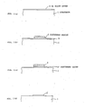
- Figs. 1(a) to 1(d) the fabrication steps in a preferred embodiment of the present invention are as follows:
- a semiconductor substrate 1 is fabricated with IC devices therein and coated with an insulation film thereon, for example of PSG (phospho silicate glass).
- a layer 2 of an aluminum-copper alloy, for example Al-Cu(4%) up to approximately 8000 ⁇ thick is formed all over the semiconductor substrate 1 by a known general method, such as sputtering, as shown in Fig. 1(a).
- a photo resist film is formed upon the alloy layer 2, and the resist film is patterned, as denoted by 3 in Fig. 1(b), by a known general lithography technique.
- the exposed portion of the alloy layer 2, i.e. the portion not masked by the photo resist pattern 3, is removed by a known general dry etching method.
- the dry etching may be a reactive ion etching method using as etching agent an etching gas such as a mixture of chlorine (Cl2) gas (24 sccm (standard cubic centimeter per minute)) and silicon tetrachloride (SiCl4) gas (40 sccm).
- etching gas such as a mixture of chlorine (Cl2) gas (24 sccm (standard cubic centimeter per minute)) and silicon tetrachloride (SiCl4) gas (40 sccm).
- the gas pressure is reduced to approximately 0.02 Torr (2.67 Pa), and radio frequency power of 13.56 MHz, for example, and 250 W, for example, is applied thereto for 5 minutes, for example, by well known methods.
- the etching gas is dissociated in a glow discharge driven by the applied radio frequency power and the chlorine atoms produced are active to react with the aluminum as well as the copper of the alloy.
- the aluminum chloride sublimes in the same manner as explained in the description of the prior art, and the copper chloride is sputtered by the energetic ion bombardment, so that the exposed portion of the alloy is etched and removed leaving the patterned layer 2 ⁇ , as shown in Fig. 1(c).
- the substrate 1 is transferred to a dry processing apparatus for stripping the patterned photo resist 3, passing through a vacuum system or an inert gas purged system, in order to avoid being exposed to the atmosphere. If the substrate is exposed to the atmosphere, the residual chlorine on the substrate reacts with water contained in the air and corrodes the alloy, as explained in the prior art.
- the patterned photo resist 3 on the patterned alloy layer 2 ⁇ is then stripped by a known downstream etching method.
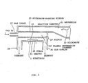
- a stripping apparatus using microwave power which is preferably employed in this stripping step, and is also called a downstream ashing or an after-glow ashing, will be described in detail later.
- a reaction gas in the dry etching a mixture of a CF4 gas (100 sccm) and oxygen (O2) gas (1500 sccm), for example, is used at approximately 1 Torr (1.33 x 10² Pa), and microwave power of 2.45 GHz and 1 KW is applied thereto for 2 minutes, for example, while the substrate is kept at room temperature, such as 30°C.
- the substrate is heated so that the residual chlorine component is baked out.
- the heating is effected by the electric heater 31 built in the stage 25 to approximately 300°C for 2 minutes for example while the apparatus is pumped out to 0.2-0.3 Torr (0.27-0.4 x 10² Pa).
- the substrate is brought out of the apparatus, thus the processes of the invention are all finished.
- This method will be referred to as method I. It is also possible to heat the substrate on a separate heating stage from the stripping stage 25 in the vacuum chamber in order to save the cycle time for heating/cooling the massive stage.
- the last baking process of method I may be combined with the stripping process. In other words, these two processes can be carried out concurrently.
- the stripping process is carried out while the substrate 1 is heated to 200 to 300°C by an electric heater 31 mounted in the stage 25. This method will be referred to as method II.
- the etching gas may be a mixture of nitrogen (N2) gas (100 sccm) and oxygen (O2) gas (1500 sccm) at approximately 1 Torr (1.33 x 10² Pa), and the substrate may be heated at 200 to 300°C.
- N2 nitrogen
- O2 oxygen
- the combination of the heating and the downstream stripping is essential, because heating without stripping cannot remove the residual chlorine components under 400°C.
- conventional plasma stripping causes a particle problem by Al2O3 formation.
- the processed substrate was exposed to the atmosphere for 2 days.
- the alloy pattern was then optically observed to check for corrosion, and the residual chlorine atoms were measured by X-ray fluorescence spectroscopy.
- the check results are set out in the following table, in which
- the temperature must be lower than 400°C, and preferably be chosen between 250 and 300°C.
- the apparatus employs microwave power for producing reactive species as etching agent.
- the substrate 1 is loaded on the stage 25 in a reaction chamber 30.
- an electric heater 31 and a thermometer (not shown in the Figure) are mounted to heat the substrate when required.
- the chamber 30 is evacuated through gas outlets 26 by conventional evacuation equipment, which is not shown in the Figure.
- An etching gas is introduced into the chamber 30 through the gas inlet 27. By balancing the gas evacuation and gas introduction, the gas pressure within the chamber 30 is controlled to obtain the required gas pressure.
- Microwave power 22 is fed through the wave guide 21 and through the microwave-passing window 23 into the plasma generation chamber 29.
- the etching gas is made into plasma by the excitation by the microwave power.
- a reactive species, such as oxygen atoms, produced in the plasma comes out through the holes of the shield plate 28 and flows directly down on to the substrate 1, i.e.
- This reactive species is very reactive with the photo resist on the substrate, but does not harm the substrate by an ionic bombardment as in the plasma etching because the species coming out of the holes of the shield plate 28 is not ionic and no other ionic gas comes out at all. Therefore, this type of apparatus is advantageously employed for stripping the photo resist.
- aluminum-copper alloy is referred to in the above-described embodiment as the material to be processed, the present invention is also effective for other alloys such as AlCuSi and AlSiTiCu.
- etching gas for etching the alloy in the above-described embodiment
- gases of chlorine family such as BCl3, CCl4 and CHCl3, can be also used therein, as is well known.
- etching gas for stripping the photo resist in the above-described embodiment
- other fluorinated gases such as CHF3, C2F6, SF6, NF3 or CBrF3
- nitrogen-containing gases such as N2O or NO2
- a dry etching apparatus using a microwave frequency of 2.45 GHz is referred to in the above-described embodiment for stripping the photo resist
- other types of dry etching apparatus e.g. using a radio frequency of 13.56 MHz, can also be used, as is well known.
Abstract
Description
- This invention relates to a method for stripping a photo resist coated on a layer of an aluminum alloy, such as aluminum-copper, formed on a semiconductor substrate.
- Aluminum or aluminum-silicon alloy containing several percent of silicon has been generally used for an interconnection layer on a semiconductor device. However, it is also well known that the interconnection layer may be broken by electromigration, particularly in a semiconductor device where a very fine interconnection is required, such as 4 µm for a high speed ECL (Emitter Coupled Logic) or 1 µm for MOS (Metal Oxide Semiconductor), to achieve a greater density of integration, and a correspondingly higher density of the current flowing therethrough is required. In order to prevent this electromigration of the interconnection layer, an aluminum-copper alloy containing 2 to 4% of copper has come to be used, particularly where a high current-density is handled as in a bipolar device or a high-speed logic circuit. However, the aluminum-copper alloy suffers from problems due to residual chlorine therein.
- When an aluminum or aluminum alloy layer is plasma dry-etched by chlorinated gases, such as a mixture of chlorine (referred to hereinafter as Cl₂) with silicon tetrachloride (SiCl₄) or boron trichloride (BCl₃), the residual chlorine problem arises as follows:
Al + Cl* → AlCl₃↑, Al₂Cl₆↑
where Cl* denotes a chlorine radical produced in the plasma, and ↑ denotes sublimation. The aluminum, Al, reacts with Cl* to produce AlCl₃ or Al₂Cl₆, which then sublimes, and the aluminum continues to be etched in this way. When the etch-processed substrate is brought out into the open air, the AlCl₃, etc., which has sublimed and deposited on a surface of the side wall of the aluminum layer or on a photo resist reacts with atmospheric water, because the AlCl₃ is deliquescent. Hydrochloric acid (HCl) is thus produced thereon as shown by the following equation:
AlCl₃ + 3 H₂O → 3 HCl + Al(OH)₃. - The HCl then reacts with the Al to produce AlCl₃ again as follows:
Al + 3 HCl → AlCl₃ + ½ H₂O. - Thus, the reactions are continued repeatedly. In other words, the corrosion of the aluminum layer continues indefinitely. In order to prevent this corrosion, one or more of the following procedures is or are carried out for aluminum, aluminum-titanium (Al-Ti) alloy or aluminum-silicon (Al-Si) alloy, after the dry etching process:
- (1) Stripping the photo resist without exposing the substrate to the open air so as to prevent the chlorine deposit on the substrate from reacting with the water content in the open air.
- (2) Drying the substrate with a hot nitrogen gas blast at up to 100 to 200°C, and then washing it with water so as to remove the residual chlorine.
- (3) Washing the substrate with water, and then baking it in an oxygen atmosphere at approximately 350°C so as to remove the residual chlorine.
- (4) Plasma-processing the substrate in a fluorinated gas, such as CF₄, SF₆ or CHF₃, so as to replace the residual chlorine atoms by the fluorine atoms produced in the plasma. A stable aluminum fluoride (AlF or AlF₃) is thus formed over the aluminum surface to prevent the chlorine component from reacting with water contained in the air.
- (5) Plasma-processing the substrate in hydrogen gas, which reacts with the residual chlorine component to produce hydrogen chloride.
- By the application of the above-mentioned procedures the residual chlorine component on the substrate made of the above-mentioned aluminum or aluminum alloys can be removed, and thus the corrosion can be prevented. However, when an aluminum alloy, such as aluminum-copper (Al-Cu) or aluminum-copper-silicon (Al-Cu-Si) is etched, its chlorine component remains in the form of CuxCly or a mixture of Cu, Cl, Al and carbon from the photo resist, which are difficult to remove as they have much higher sublimation temperatures than aluminum chloride, and may therefore cause corrosion even after the above-described chlorine-removal processing is carried out.
- To overcome the above-mentioned problems an improved method of removing the residual chlorine is desirable.
- It is an object of the invention to provide a method that may be used to form a pattern of an aluminum alloy on a semiconductor substrate without corrosion problems caused by residual chlorine on the substrate.
- According to the invention, a method for etching an aluminum alloy pattern on a semiconductor substrate comprises the steps of:
forming a layer of aluminum alloy on a semiconductor substrate having an insulation layer thereon;
forming a resist pattern on said aluminum alloy layer;
etching an exposed portion of said aluminum alloy layer by the use of said resist pattern as a mask, whereby said aluminum alloy layer is patterned;
stripping said resist pattern in an atmosphere containing a reactive species; and
heating the substrate in a vacuum at a temperature higher than 100°C, whereby residual etching agent on the substrate is removed, said heating step being carried out concurrently with said stripping step or after said stripping step. - In an embodiment of the invention, the method includes the steps of: forming a layer of aluminum-copper alloy on a semiconductor substrate; forming a resist pattern on said alloy layer; etching said alloy layer by the use of said resist pattern in a chlorinated gas plasma so as to form an alloy pattern; downstream stripping said resist pattern in an atmosphere containing a reactive species; and heating the thus-processed substrate in a vacuum at a temperature higher than 100°C, to remove the residual chlorine component. The stripping process and the heating process may be combined; that is to say, be carried out concurrently.
- The above-mentioned features and advantages of the present invention, together with other objects and advantages, which will become apparent, will be more fully described hereinafter with reference to the accompanying drawings, in which like numerals refer to like parts throughout.
- Figs. 1(a) to 1(d) are sectional views that schematically illustrate the main part of a semiconductor device at successive steps of a fabrication process according to the present invention.
- Fig. 2 schematically illustrates a dry processing apparatus using microwave power, used for the stripping step of the present invention.
- Referring now to Figs. 1(a) to 1(d), the fabrication steps in a preferred embodiment of the present invention are as follows:
- By general fabrication methods (not shown in the Figures) a
semiconductor substrate 1 is fabricated with IC devices therein and coated with an insulation film thereon, for example of PSG (phospho silicate glass). Alayer 2 of an aluminum-copper alloy, for example Al-Cu(4%) up to approximately 8000Å thick is formed all over thesemiconductor substrate 1 by a known general method, such as sputtering, as shown in Fig. 1(a). A photo resist film is formed upon thealloy layer 2, and the resist film is patterned, as denoted by 3 in Fig. 1(b), by a known general lithography technique. The exposed portion of thealloy layer 2, i.e. the portion not masked by thephoto resist pattern 3, is removed by a known general dry etching method. The dry etching may be a reactive ion etching method using as etching agent an etching gas such as a mixture of chlorine (Cl₂) gas (24 sccm (standard cubic centimeter per minute)) and silicon tetrachloride (SiCl₄) gas (40 sccm). The gas pressure is reduced to approximately 0.02 Torr (2.67 Pa), and radio frequency power of 13.56 MHz, for example, and 250 W, for example, is applied thereto for 5 minutes, for example, by well known methods. The etching gas is dissociated in a glow discharge driven by the applied radio frequency power and the chlorine atoms produced are active to react with the aluminum as well as the copper of the alloy. The aluminum chloride sublimes in the same manner as explained in the description of the prior art, and the copper chloride is sputtered by the energetic ion bombardment, so that the exposed portion of the alloy is etched and removed leaving the patterned layer 2ʹ, as shown in Fig. 1(c). Next, thesubstrate 1 is transferred to a dry processing apparatus for stripping the patternedphoto resist 3, passing through a vacuum system or an inert gas purged system, in order to avoid being exposed to the atmosphere. If the substrate is exposed to the atmosphere, the residual chlorine on the substrate reacts with water contained in the air and corrodes the alloy, as explained in the prior art. - The patterned photo resist 3 on the patterned alloy layer 2ʹ is then stripped by a known downstream etching method. A stripping apparatus using microwave power, which is preferably employed in this stripping step, and is also called a downstream ashing or an after-glow ashing, will be described in detail later. As a reaction gas in the dry etching, a mixture of a CF₄ gas (100 sccm) and oxygen (O₂) gas (1500 sccm), for example, is used at approximately 1 Torr (1.33 x 10² Pa), and microwave power of 2.45 GHz and 1 KW is applied thereto for 2 minutes, for example, while the substrate is kept at room temperature, such as 30°C. After finishing this stripping process, the substrate is heated so that the residual chlorine component is baked out. In the apparatus shown in Fig.2 the heating is effected by the electric heater 31 built in the stage 25 to approximately 300°C for 2 minutes for example while the apparatus is pumped out to 0.2-0.3 Torr (0.27-0.4 x 10² Pa). After the substrate is cooled enough, the substrate is brought out of the apparatus, thus the processes of the invention are all finished. This method will be referred to as method I. It is also possible to heat the substrate on a separate heating stage from the stripping stage 25 in the vacuum chamber in order to save the cycle time for heating/cooling the massive stage.
- The last baking process of method I may be combined with the stripping process. In other words, these two processes can be carried out concurrently. In this case, the stripping process is carried out while the
substrate 1 is heated to 200 to 300°C by an electric heater 31 mounted in the stage 25. This method will be referred to as method II. - When the stripping and baking processes are combined as in method II, the etching gas may be a mixture of nitrogen (N₂) gas (100 sccm) and oxygen (O₂) gas (1500 sccm) at approximately 1 Torr (1.33 x 10² Pa), and the substrate may be heated at 200 to 300°C. This method will be referred to as method III.
- In these methods, the combination of the heating and the downstream stripping is essential, because heating without stripping cannot remove the residual chlorine components under 400°C. Moreover, conventional plasma stripping causes a particle problem by Al₂O₃ formation.
- In order to confirm the effect of the above-described methods of the present invention, the processed substrate was exposed to the atmosphere for 2 days. The alloy pattern was then optically observed to check for corrosion, and the residual chlorine atoms were measured by X-ray fluorescence spectroscopy. The check results are set out in the following table, in which
- (a) shows the temperature of the substrate during the heating, in °C,
- (b) shows existence of the corrosion found by optical observation using a microscope of magnification x 1000, and
- (c) shows the amount of residual chlorine atoms in units of cps (counts per second), where 10-cps corresponds to 1.64 x 10⁴ atoms per cm².
- As seen in the Table, when the substrate is heated at above 100°C, the residual chlorine is evidently reduced and no corrosion is observed. The amount of residual chlorine is reduced as the heating temperature is raised, but on the other hand, if the temperature exceeds 300°C, the aluminum is affected: for example hillocks are formed on the surface of the aluminum. Therefore, the temperature must be lower than 400°C, and preferably be chosen between 250 and 300°C.
- An embodiment of the dry etching apparatus for stripping the photo resist will now be described in detail, with reference to Fig. 2. The apparatus employs microwave power for producing reactive species as etching agent. The
substrate 1 is loaded on the stage 25 in areaction chamber 30. In the stage 25, an electric heater 31 and a thermometer (not shown in the Figure) are mounted to heat the substrate when required. Thechamber 30 is evacuated throughgas outlets 26 by conventional evacuation equipment, which is not shown in the Figure. An etching gas is introduced into thechamber 30 through thegas inlet 27. By balancing the gas evacuation and gas introduction, the gas pressure within thechamber 30 is controlled to obtain the required gas pressure. A microwave-passingwindow 23 made of an insulating material, such as quartz or alumina, is installed perpendicularly to the electric field in thewave guide 21 and also seals the vacuum of thechamber 30. Ametal shield plate 28 having many small holes therein shields the microwaves from thereaction chamber 30, so that aplasma generation chamber 29 is formed between the microwave-passingwindow 23 and theshield plate 28.Microwave power 22 is fed through thewave guide 21 and through the microwave-passingwindow 23 into theplasma generation chamber 29. In theplasma generation chamber 29, the etching gas is made into plasma by the excitation by the microwave power. A reactive species, such as oxygen atoms, produced in the plasma comes out through the holes of theshield plate 28 and flows directly down on to thesubstrate 1, i.e. efficiently, because the shield plate is located close to thesubstrate 1. This reactive species is very reactive with the photo resist on the substrate, but does not harm the substrate by an ionic bombardment as in the plasma etching because the species coming out of the holes of theshield plate 28 is not ionic and no other ionic gas comes out at all. Therefore, this type of apparatus is advantageously employed for stripping the photo resist. - Although aluminum-copper alloy is referred to in the above-described embodiment as the material to be processed, the present invention is also effective for other alloys such as AlCuSi and AlSiTiCu.
- Although a mixture of Cl₂ and SiCl₄ is referred to as an etching gas for etching the alloy in the above-described embodiment, other gases of chlorine family, such as BCl₃, CCl₄ and CHCl₃, can be also used therein, as is well known.
- Although a dry etching apparatus using a radio frequency of 13.56 MHz is referred to in the above-described embodiment for etching the alloy, other types of dry etching apparatus, for example using a radio frequency of 400 KHz, can also be used, as is well known.
- Although a mixture of CF₄, N₂ and O₂ is referred to as an etching gas for stripping the photo resist in the above-described embodiment, other fluorinated gases, such as CHF₃, C₂F₆, SF₆, NF₃ or CBrF₃, can be also used, singly or mixed, in place of CF₄, and other nitrogen-containing gases, such as N₂O or NO₂, can be also used in place of N₂, as is well known.
- Although a dry etching apparatus using a microwave frequency of 2.45 GHz is referred to in the above-described embodiment for stripping the photo resist, other types of dry etching apparatus, e.g. using a radio frequency of 13.56 MHz, can also be used, as is well known.
- The many features and advantages of the invention are apparent from the detailed specification. Further, since numerous modifications and changes will readily occur to those skilled in the art, it is not desired to limit the invention to the exact construction and operation shown and described, and accordingly, all suitable modifications and equivalents may be resorted to, falling within the scope of the invention as claimed.

Claims (9)
forming a layer of aluminum alloy on a semiconductor substrate having an insulation layer thereon;
forming a resist pattern on said aluminum alloy layer;
etching an exposed portion of said aluminum alloy layer by the use of said resist pattern as a mask, whereby said aluminum alloy layer is patterned;
stripping said resist pattern in an atmosphere containing a reactive species; and heating the substrate in a vacuum at a temperature higher than 100°C, whereby residual etching agent on the substrate is removed, said heating step being carried out concurrently with said stripping step or after said stripping step.
Applications Claiming Priority (3)
| Application Number | Priority Date | Filing Date | Title |
|---|---|---|---|
| JP124123/86 | 1986-05-29 | ||
| JP12412386 | 1986-05-29 | ||
| JP61124123A JPS62281331A (en) | 1986-05-29 | 1986-05-29 | Etching method |
Publications (3)
| Publication Number | Publication Date |
|---|---|
| EP0247603A2 true EP0247603A2 (en) | 1987-12-02 |
| EP0247603A3 EP0247603A3 (en) | 1988-07-20 |
| EP0247603B1 EP0247603B1 (en) | 1999-08-25 |
Family
ID=14877494
Family Applications (1)
| Application Number | Title | Priority Date | Filing Date |
|---|---|---|---|
| EP87107743A Expired - Lifetime EP0247603B1 (en) | 1986-05-29 | 1987-05-27 | A method for stripping a photo resist on an aluminium alloy |
Country Status (5)
| Country | Link |
|---|---|
| US (2) | US6184148B1 (en) |
| EP (1) | EP0247603B1 (en) |
| JP (1) | JPS62281331A (en) |
| KR (2) | KR870011678A (en) |
| DE (1) | DE3752290T2 (en) |
Cited By (12)
| Publication number | Priority date | Publication date | Assignee | Title |
|---|---|---|---|---|
| EP0416774A1 (en) * | 1989-08-28 | 1991-03-13 | Hitachi, Ltd. | A method of treating a sample of aluminium-containing material |
| DE4040061A1 (en) * | 1990-07-04 | 1992-01-23 | Mitsubishi Electric Corp | METHOD FOR PRODUCING A STRUCTURED LINKING LAYER |
| EP0485802A1 (en) * | 1990-10-30 | 1992-05-20 | Nec Corporation | Method of preventing corrosion of aluminium alloys |
| EP0651437A2 (en) * | 1993-10-29 | 1995-05-03 | Applied Materials, Inc. | Plasma etch process |
| FR2720854A1 (en) * | 1993-12-28 | 1995-12-08 | Fujitsu Ltd | Mfr. of semiconductor device with an aluminium@ wiring layer |
| EP0709877A1 (en) * | 1993-05-20 | 1996-05-01 | Hitachi, Ltd. | Plasma processing method |
| WO1999004606A2 (en) * | 1997-07-14 | 1999-01-28 | Lam Research Corporation | Compact microwave downstream plasma system |
| US5868854A (en) * | 1989-02-27 | 1999-02-09 | Hitachi, Ltd. | Method and apparatus for processing samples |
| GB2339494A (en) * | 1998-07-09 | 2000-01-26 | Nec Corp | Patterning conductive lines without after-corrosion |
| US6060397A (en) * | 1995-07-14 | 2000-05-09 | Applied Materials, Inc. | Gas chemistry for improved in-situ cleaning of residue for a CVD apparatus |
| US6077788A (en) * | 1989-02-27 | 2000-06-20 | Hitachi, Ltd. | Method and apparatus for processing samples |
| US6989228B2 (en) | 1989-02-27 | 2006-01-24 | Hitachi, Ltd | Method and apparatus for processing samples |
Families Citing this family (12)
| Publication number | Priority date | Publication date | Assignee | Title |
|---|---|---|---|---|
| JP2728483B2 (en) * | 1989-02-01 | 1998-03-18 | 株式会社日立製作所 | Sample post-treatment method and device |
| US6451217B1 (en) * | 1998-06-09 | 2002-09-17 | Speedfam-Ipec Co., Ltd. | Wafer etching method |
| US20050022839A1 (en) * | 1999-10-20 | 2005-02-03 | Savas Stephen E. | Systems and methods for photoresist strip and residue treatment in integrated circuit manufacturing |
| US6660646B1 (en) * | 2000-09-21 | 2003-12-09 | Northrop Grumman Corporation | Method for plasma hardening photoresist in etching of semiconductor and superconductor films |
| US20020142612A1 (en) * | 2001-03-30 | 2002-10-03 | Han-Ming Wu | Shielding plate in plasma for uniformity improvement |
| KR100928098B1 (en) * | 2002-12-24 | 2009-11-24 | 동부일렉트로닉스 주식회사 | Metal line formation method using oxide film |
| US20070193602A1 (en) * | 2004-07-12 | 2007-08-23 | Savas Stephen E | Systems and Methods for Photoresist Strip and Residue Treatment in Integrated Circuit Manufacturing |
| KR100734778B1 (en) | 2005-08-25 | 2007-07-03 | 세메스 주식회사 | apparatus and method for treating a substrate by plasma |
| US20080061112A1 (en) * | 2006-09-07 | 2008-03-13 | Shih-Ju Liang | Method for soldering charge coupled device and tooling thereof |
| CN102226635B (en) * | 2011-06-09 | 2013-02-27 | 四川宏普微波科技有限公司 | Microwave continuous freeze-drying device |
| CN102929110B (en) * | 2012-11-06 | 2014-03-19 | 中国科学院微电子研究所 | Device and method for supercritical drying of microwave excitation |
| US10866516B2 (en) | 2016-08-05 | 2020-12-15 | Taiwan Semiconductor Manufacturing Co., Ltd. | Metal-compound-removing solvent and method in lithography |
Citations (5)
| Publication number | Priority date | Publication date | Assignee | Title |
|---|---|---|---|---|
| EP0010138A1 (en) * | 1978-09-25 | 1980-04-30 | International Business Machines Corporation | A method of treating aluminium microcircuits |
| JPS5655050A (en) * | 1979-10-11 | 1981-05-15 | Fujitsu Ltd | Manufacture of semiconductor device |
| US4370195A (en) * | 1982-03-25 | 1983-01-25 | Rca Corporation | Removal of plasma etching residues |
| JPS593927A (en) * | 1982-06-29 | 1984-01-10 | Fujitsu Ltd | Etching of thin film |
| JPS59186326A (en) * | 1983-04-06 | 1984-10-23 | Hitachi Ltd | Dry-etching apparatus |
Family Cites Families (12)
| Publication number | Priority date | Publication date | Assignee | Title |
|---|---|---|---|---|
| JPS53112065A (en) * | 1977-03-11 | 1978-09-30 | Toshiba Corp | Removing method of high molecular compound |
| JPS57170534A (en) * | 1981-04-15 | 1982-10-20 | Hitachi Ltd | Dry etching method for aluminum and aluminum alloy |
| US4718976A (en) * | 1982-03-31 | 1988-01-12 | Fujitsu Limited | Process and apparatus for plasma treatment |
| JPS59210644A (en) * | 1983-05-16 | 1984-11-29 | Oki Electric Ind Co Ltd | Manufacture of semiconductor device |
| JPS6016424A (en) * | 1983-07-08 | 1985-01-28 | Fujitsu Ltd | Microwave plasma processing method and apparatus thereof |
| JPS6130036A (en) * | 1984-07-23 | 1986-02-12 | Fujitsu Ltd | Microwave plasma processing apparatus |
| US4592800A (en) * | 1984-11-02 | 1986-06-03 | Oerlikon-Buhrle U.S.A. Inc. | Method of inhibiting corrosion after aluminum etching |
| US4631105A (en) * | 1985-04-22 | 1986-12-23 | Branson International Plasma Corporation | Plasma etching apparatus |
| US4699689A (en) * | 1985-05-17 | 1987-10-13 | Emergent Technologies Corporation | Method and apparatus for dry processing of substrates |
| JPH0722153B2 (en) * | 1985-09-09 | 1995-03-08 | 日本電信電話株式会社 | Dry etching method and apparatus |
| US4632719A (en) * | 1985-09-18 | 1986-12-30 | Varian Associates, Inc. | Semiconductor etching apparatus with magnetic array and vertical shield |
| US4662977A (en) * | 1986-05-05 | 1987-05-05 | University Patents, Inc. | Neutral particle surface alteration |
-
1986
- 1986-05-29 JP JP61124123A patent/JPS62281331A/en active Granted
-
1987
- 1987-05-27 EP EP87107743A patent/EP0247603B1/en not_active Expired - Lifetime
- 1987-05-27 DE DE3752290T patent/DE3752290T2/en not_active Expired - Fee Related
- 1987-05-29 KR KR1019870005360A patent/KR870011678A/en not_active IP Right Cessation
- 1987-05-29 KR KR1019870005360A patent/KR900004053B1/en active
-
1997
- 1997-04-18 US US08/839,371 patent/US6184148B1/en not_active Expired - Fee Related
-
2000
- 2000-08-16 US US09/639,113 patent/US6486073B1/en not_active Expired - Fee Related
Patent Citations (5)
| Publication number | Priority date | Publication date | Assignee | Title |
|---|---|---|---|---|
| EP0010138A1 (en) * | 1978-09-25 | 1980-04-30 | International Business Machines Corporation | A method of treating aluminium microcircuits |
| JPS5655050A (en) * | 1979-10-11 | 1981-05-15 | Fujitsu Ltd | Manufacture of semiconductor device |
| US4370195A (en) * | 1982-03-25 | 1983-01-25 | Rca Corporation | Removal of plasma etching residues |
| JPS593927A (en) * | 1982-06-29 | 1984-01-10 | Fujitsu Ltd | Etching of thin film |
| JPS59186326A (en) * | 1983-04-06 | 1984-10-23 | Hitachi Ltd | Dry-etching apparatus |
Non-Patent Citations (4)
| Title |
|---|
| IBM TECHNICAL DISCLOSURE BULLETIN, vol. 21, no. 6, November 1978, page 2315, New York, US; G.T. CHIU et al.: "Plasma removal of residue following reactive ion etching of aluminum and aluminum alloys" * |
| PATENT ABSTRACTS OF JAPAN, vol. 5, no. 117 (E-67)[789], 28th July 1981; & JP-A-56 055 050 (FUJITSU K.K.) 15-05-1981 * |
| PATENT ABSTRACTS OF JAPAN, vol. 8, no. 81 (E-238)[1518], 13th April 1984; & JP-A-59 003 927 (FUJITSU K.K.) 10-01-1984 * |
| PATENT ABSTRACTS OF JAPAN, vol. 9, no. 47 (E-299)[1770], 27th February 1985; & JP-A-59 186 326 (HITACHI SEISAKUSHO K.K.) 23-10-1984 * |
Cited By (26)
| Publication number | Priority date | Publication date | Assignee | Title |
|---|---|---|---|---|
| US6077788A (en) * | 1989-02-27 | 2000-06-20 | Hitachi, Ltd. | Method and apparatus for processing samples |
| US6254721B1 (en) | 1989-02-27 | 2001-07-03 | Hitachi, Ltd. | Method and apparatus for processing samples |
| US5868854A (en) * | 1989-02-27 | 1999-02-09 | Hitachi, Ltd. | Method and apparatus for processing samples |
| US5952245A (en) * | 1989-02-27 | 1999-09-14 | Hitachi, Ltd. | Method for processing samples |
| US6036816A (en) * | 1989-02-27 | 2000-03-14 | Hitachi, Ltd. | Apparatus for processing a sample having a metal laminate |
| US6989228B2 (en) | 1989-02-27 | 2006-01-24 | Hitachi, Ltd | Method and apparatus for processing samples |
| US6656846B2 (en) | 1989-02-27 | 2003-12-02 | Hitachi, Ltd. | Apparatus for processing samples |
| US6537415B2 (en) | 1989-02-27 | 2003-03-25 | Hitachi, Ltd. | Apparatus for processing samples |
| US6537417B2 (en) | 1989-02-27 | 2003-03-25 | Hitachi, Ltd. | Apparatus for processing samples |
| US7132293B2 (en) | 1989-02-27 | 2006-11-07 | Hitachi, Ltd. | Method and apparatus for processing samples |
| US5380397A (en) * | 1989-08-28 | 1995-01-10 | Hitachi, Ltd. | Method of treating samples |
| US6329298B1 (en) | 1989-08-28 | 2001-12-11 | Hitachi, Ltd. | Apparatus for treating samples |
| US5556714A (en) * | 1989-08-28 | 1996-09-17 | Hitachi, Ltd. | Method of treating samples |
| EP0416774A1 (en) * | 1989-08-28 | 1991-03-13 | Hitachi, Ltd. | A method of treating a sample of aluminium-containing material |
| DE4040061A1 (en) * | 1990-07-04 | 1992-01-23 | Mitsubishi Electric Corp | METHOD FOR PRODUCING A STRUCTURED LINKING LAYER |
| US5198388A (en) * | 1990-07-04 | 1993-03-30 | Mitsubishi Denki Kabushiki Kaisha | Method of forming interconnection patterns |
| EP0485802A1 (en) * | 1990-10-30 | 1992-05-20 | Nec Corporation | Method of preventing corrosion of aluminium alloys |
| EP0709877A4 (en) * | 1993-05-20 | 1997-11-26 | Hitachi Ltd | Plasma processing method |
| EP0709877A1 (en) * | 1993-05-20 | 1996-05-01 | Hitachi, Ltd. | Plasma processing method |
| EP0651437A3 (en) * | 1993-10-29 | 1996-04-17 | Applied Materials Inc | Plasma etch process. |
| EP0651437A2 (en) * | 1993-10-29 | 1995-05-03 | Applied Materials, Inc. | Plasma etch process |
| FR2720854A1 (en) * | 1993-12-28 | 1995-12-08 | Fujitsu Ltd | Mfr. of semiconductor device with an aluminium@ wiring layer |
| US6060397A (en) * | 1995-07-14 | 2000-05-09 | Applied Materials, Inc. | Gas chemistry for improved in-situ cleaning of residue for a CVD apparatus |
| WO1999004606A2 (en) * | 1997-07-14 | 1999-01-28 | Lam Research Corporation | Compact microwave downstream plasma system |
| WO1999004606A3 (en) * | 1997-07-14 | 1999-04-22 | Lam Res Corp | Compact microwave downstream plasma system |
| GB2339494A (en) * | 1998-07-09 | 2000-01-26 | Nec Corp | Patterning conductive lines without after-corrosion |
Also Published As
| Publication number | Publication date |
|---|---|
| JPS62281331A (en) | 1987-12-07 |
| EP0247603B1 (en) | 1999-08-25 |
| DE3752290D1 (en) | 1999-09-30 |
| DE3752290T2 (en) | 2000-01-27 |
| US6184148B1 (en) | 2001-02-06 |
| KR900004053B1 (en) | 1990-06-09 |
| JPH057862B2 (en) | 1993-01-29 |
| EP0247603A3 (en) | 1988-07-20 |
| KR870011678A (en) | 1987-12-26 |
| US6486073B1 (en) | 2002-11-26 |
Similar Documents
| Publication | Publication Date | Title |
|---|---|---|
| EP0247603A2 (en) | A method for stripping a photo resist on an aluminium alloy | |
| US4028155A (en) | Process and material for manufacturing thin film integrated circuits | |
| US4547260A (en) | Process for fabricating a wiring layer of aluminum or aluminum alloy on semiconductor devices | |
| EP0416774B1 (en) | A method of treating a sample of aluminium-containing material | |
| JP3090476B2 (en) | Method of forming silicon fluoride oxide layer using plasma enhanced chemical vapor deposition | |
| EP0489179B1 (en) | Method of manufacturing semiconductor integrated circuit | |
| KR100255960B1 (en) | Uv-enhanced dry stripping method of silicon nitride films | |
| KR900003256B1 (en) | Method of removing photo resist on a semiconductor wafer | |
| US6346489B1 (en) | Precleaning process for metal plug that minimizes damage to low-κ dielectric | |
| US7202176B1 (en) | Enhanced stripping of low-k films using downstream gas mixing | |
| EP0047002A2 (en) | Plasma etching apparatus | |
| EP0665583A2 (en) | Method of etching titanium nitride and insulating oxide layers using a gas comprising carbon-fluoride and carbon-oxide. | |
| EP0019915B1 (en) | Method for preventing the corrosion of al and al alloys | |
| JP2000012514A (en) | Post-treating method | |
| US4229247A (en) | Glow discharge etching process for chromium | |
| EP1655771A1 (en) | Method for forming film, method for manufacturing semiconductor device, semiconductor device and substrate treatment system | |
| US5211804A (en) | Method for dry etching | |
| US6162733A (en) | Method for removing contaminants from integrated circuits | |
| EP1143498A2 (en) | Post etch photoresist and residue removal process | |
| KR950005351B1 (en) | Method of preventing corrosion of aluminum alloys | |
| EP1074043A1 (en) | Process for ashing organic materials from substrates | |
| Jimbo et al. | Resist and sidewall film removal after Al reactive ion etching (RIE) employing F+ H2O downstream ashing | |
| JPH0793293B2 (en) | Post-processing method | |
| JP3298234B2 (en) | Wiring formation method | |
| JP3403595B2 (en) | Processing method of wiring material |
Legal Events
| Date | Code | Title | Description |
|---|---|---|---|
| PUAI | Public reference made under article 153(3) epc to a published international application that has entered the european phase |
Free format text: ORIGINAL CODE: 0009012 |
|
| AK | Designated contracting states |
Kind code of ref document: A2 Designated state(s): DE FR GB |
|
| PUAL | Search report despatched |
Free format text: ORIGINAL CODE: 0009013 |
|
| AK | Designated contracting states |
Kind code of ref document: A3 Designated state(s): DE FR GB |
|
| 17P | Request for examination filed |
Effective date: 19881209 |
|
| 17Q | First examination report despatched |
Effective date: 19910625 |
|
| APAB | Appeal dossier modified |
Free format text: ORIGINAL CODE: EPIDOS NOAPE |
|
| GRAG | Despatch of communication of intention to grant |
Free format text: ORIGINAL CODE: EPIDOS AGRA |
|
| GRAH | Despatch of communication of intention to grant a patent |
Free format text: ORIGINAL CODE: EPIDOS IGRA |
|
| GRAG | Despatch of communication of intention to grant |
Free format text: ORIGINAL CODE: EPIDOS AGRA |
|
| GRAH | Despatch of communication of intention to grant a patent |
Free format text: ORIGINAL CODE: EPIDOS IGRA |
|
| GRAG | Despatch of communication of intention to grant |
Free format text: ORIGINAL CODE: EPIDOS AGRA |
|
| GRAG | Despatch of communication of intention to grant |
Free format text: ORIGINAL CODE: EPIDOS AGRA |
|
| GRAH | Despatch of communication of intention to grant a patent |
Free format text: ORIGINAL CODE: EPIDOS IGRA |
|
| GRAG | Despatch of communication of intention to grant |
Free format text: ORIGINAL CODE: EPIDOS AGRA |
|
| GRAH | Despatch of communication of intention to grant a patent |
Free format text: ORIGINAL CODE: EPIDOS IGRA |
|
| GRAH | Despatch of communication of intention to grant a patent |
Free format text: ORIGINAL CODE: EPIDOS IGRA |
|
| GRAA | (expected) grant |
Free format text: ORIGINAL CODE: 0009210 |
|
| AK | Designated contracting states |
Kind code of ref document: B1 Designated state(s): DE FR GB |
|
| REF | Corresponds to: |
Ref document number: 3752290 Country of ref document: DE Date of ref document: 19990930 |
|
| ET | Fr: translation filed | ||
| PLBE | No opposition filed within time limit |
Free format text: ORIGINAL CODE: 0009261 |
|
| STAA | Information on the status of an ep patent application or granted ep patent |
Free format text: STATUS: NO OPPOSITION FILED WITHIN TIME LIMIT |
|
| 26N | No opposition filed | ||
| REG | Reference to a national code |
Ref country code: GB Ref legal event code: IF02 |
|
| PGFP | Annual fee paid to national office [announced via postgrant information from national office to epo] |
Ref country code: FR Payment date: 20050511 Year of fee payment: 19 |
|
| PGFP | Annual fee paid to national office [announced via postgrant information from national office to epo] |
Ref country code: DE Payment date: 20050519 Year of fee payment: 19 |
|
| PGFP | Annual fee paid to national office [announced via postgrant information from national office to epo] |
Ref country code: GB Payment date: 20050525 Year of fee payment: 19 |
|
| APAH | Appeal reference modified |
Free format text: ORIGINAL CODE: EPIDOSCREFNO |
|
| PG25 | Lapsed in a contracting state [announced via postgrant information from national office to epo] |
Ref country code: GB Free format text: LAPSE BECAUSE OF NON-PAYMENT OF DUE FEES Effective date: 20060527 |
|
| PG25 | Lapsed in a contracting state [announced via postgrant information from national office to epo] |
Ref country code: DE Free format text: LAPSE BECAUSE OF NON-PAYMENT OF DUE FEES Effective date: 20061201 |
|
| GBPC | Gb: european patent ceased through non-payment of renewal fee |
Effective date: 20060527 |
|
| REG | Reference to a national code |
Ref country code: FR Ref legal event code: ST Effective date: 20070131 |
|
| PG25 | Lapsed in a contracting state [announced via postgrant information from national office to epo] |
Ref country code: FR Free format text: LAPSE BECAUSE OF NON-PAYMENT OF DUE FEES Effective date: 20060531 |