EP0249986B1 - Analog-to-digital converter - Google Patents
Analog-to-digital converter Download PDFInfo
- Publication number
- EP0249986B1 EP0249986B1 EP87108802A EP87108802A EP0249986B1 EP 0249986 B1 EP0249986 B1 EP 0249986B1 EP 87108802 A EP87108802 A EP 87108802A EP 87108802 A EP87108802 A EP 87108802A EP 0249986 B1 EP0249986 B1 EP 0249986B1
- Authority
- EP
- European Patent Office
- Prior art keywords
- converter
- digital
- capacitors
- analog
- input
- Prior art date
- Legal status (The legal status is an assumption and is not a legal conclusion. Google has not performed a legal analysis and makes no representation as to the accuracy of the status listed.)
- Expired - Lifetime
Links
Images


Classifications
-
- H—ELECTRICITY
- H03—ELECTRONIC CIRCUITRY
- H03M—CODING; DECODING; CODE CONVERSION IN GENERAL
- H03M1/00—Analogue/digital conversion; Digital/analogue conversion
- H03M1/06—Continuously compensating for, or preventing, undesired influence of physical parameters
- H03M1/0617—Continuously compensating for, or preventing, undesired influence of physical parameters characterised by the use of methods or means not specific to a particular type of detrimental influence
- H03M1/0675—Continuously compensating for, or preventing, undesired influence of physical parameters characterised by the use of methods or means not specific to a particular type of detrimental influence using redundancy
- H03M1/0678—Continuously compensating for, or preventing, undesired influence of physical parameters characterised by the use of methods or means not specific to a particular type of detrimental influence using redundancy using additional components or elements, e.g. dummy components
-
- H—ELECTRICITY
- H03—ELECTRONIC CIRCUITRY
- H03M—CODING; DECODING; CODE CONVERSION IN GENERAL
- H03M1/00—Analogue/digital conversion; Digital/analogue conversion
- H03M1/12—Analogue/digital converters
- H03M1/34—Analogue value compared with reference values
- H03M1/38—Analogue value compared with reference values sequentially only, e.g. successive approximation type
- H03M1/46—Analogue value compared with reference values sequentially only, e.g. successive approximation type with digital/analogue converter for supplying reference values to converter
- H03M1/466—Analogue value compared with reference values sequentially only, e.g. successive approximation type with digital/analogue converter for supplying reference values to converter using switched capacitors
- H03M1/468—Analogue value compared with reference values sequentially only, e.g. successive approximation type with digital/analogue converter for supplying reference values to converter using switched capacitors in which the input S/H circuit is merged with the feedback DAC array
-
- H—ELECTRICITY
- H03—ELECTRONIC CIRCUITRY
- H03M—CODING; DECODING; CODE CONVERSION IN GENERAL
- H03M1/00—Analogue/digital conversion; Digital/analogue conversion
- H03M1/66—Digital/analogue converters
- H03M1/74—Simultaneous conversion
- H03M1/80—Simultaneous conversion using weighted impedances
- H03M1/802—Simultaneous conversion using weighted impedances using capacitors, e.g. neuron-mos transistors, charge coupled devices
- H03M1/804—Simultaneous conversion using weighted impedances using capacitors, e.g. neuron-mos transistors, charge coupled devices with charge redistribution
Definitions
- the present invention relates to an analog-to-digital converter, and more specifically to a successive approximation type analog-to-digital converter which includes a plurality of local digital-to-analog converters of a given resolution and which can provide a resolution higher than the given resolution of the digital-to-analog converter.
- GB-A-2 102 227 shows an analog-to-digital-converter of this king having two local DAC's of different size being controlled by a successive approximation register.
- EP-A-0 066 251 shows a local DAC comprising means for dividing the input-digital signal into a plurality of digital signals of smaller bit size than the input signal, a corresponding plurality of DAC's for converting these signals into analog output signals and means for summing the analog output signals to produce a summed analog output signal.
- a local DAC is described in connection with Fig. 4 of the present application.
- analog-to-digital converters called “A/D converter” hereinafter
- D/A converter digital-to-analog converter
- a successive approximation type A/D converter is known as one which can operate at an intermediate or high speed and can provide a digital signal composed of a relatively large number of bits.
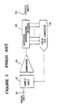
- FIG. 1 there is shown a block diagram of a typical example of a conventional successive approximation type A/D converter.
- the shown A/D converter includes an analog signal input terminal 10 connected to a first input of a sample and hold circuit 12, which has a second input connected to an output of a local D/Aconverter 14.
- the sample and hold circuit 12 has a pair of outputs corresponding to the pair of inputs, these outputs being connected to a pair of inputs of a comparator 16, whose output is connected to a successive approximation register 18.
- This register 18 has parallel outputs connected to the local D/A converter 14. Further, a serial output of the register 18 is connected to a digital signal output terminal 20.
- the local D/A converter is so set to generate a voltage V Fs /2 corresponding to a half of the full scale voltage V FS when it receives the parallel output of the register 18 composed of the most significant bit (MSB) of "1" and the other bits of "0".
- MSB most significant bit
- the voltage of the analog signal held in the sample and hold circuit 12 is compared with the output voltage V Fs /2 of the local D/Aconverter by the comparator 16.
- the result of comparison is outputted to the successive approximation register 18, which changes its content, i.e., a digital data to be supplied to the local D/A converter 14.
- the value of the MSB is determined, and then, the next comparison is made between the input analog signal and the reference voltage V Fs /4 or 3V Fs /4 of the local D/Aconverter 14, so that the 2SB will be determined.
- similar operation will be repeated to successively determine each bit of the digital data until the least significant bit (LSB) is determined.
- the local D/Aconverter is generally divided into two types, one of which includes a resistor string or ladder and the other of which includes a capacitor array.
- D/A converters which have a resolution of 8 bits to 10 bits and which can be used as the local D/A converter 14 in the above mentioned conventional successive approximation A/D converter, can be manufactured in mass production manner with high reliability and stability in accordance with recent advanced integrated circuit technique. Therefore, A/D converters having a relatively small bit number can be manufactured with reliability.
- components fabricated on an integrated circuit have a certain limit in uniformity of characteristics, and therefore, it is the present status that it is difficult to obtain a D/A converter having a higher resolution.
- a D/A converter having a resolution of 12 bits to 16 bits it is necessary to constitute a circuit with discrete parts such as resistors and capacitors of the accuracy matching with the required resolution. Otherwise, it is necessary to use a fine adjustment means such as a Laser trimming. In this case, however, the cost for forming required elements becomes very large, and also, elements having a sufficient reliability cannot be obtained.
- the first unitary D/A converter will increment its output in response to increment of a digital input.
- the MSB of the digital input changes from “0" to "1”
- the logic value "1” is supplied to all input bits of the first unitary D/A converter so that it outputs its full scale FS1.
- the second unitary D/Aconverter will increment in response to increment of the digital input, so that the output of the second D/A converter is added to the output of the first D/A converter to provide a combined output.
- the first mentioned accumulation method using a plurality of unitary D/A converters in parallel is disadvantageous in that a gain error of each unitary D/A converter is accumulated, with the result that the overall D/A converter has a large error in total linearity.
- the interpolation type has such a defect that it cannot have a monotonic increase if a slave D/A converter has an increased step error.
- Another object of the present invention is to provide a successive approximation A/D converter which uses a plurality of D/A converters but which does not have a large gain error as a whole.
- a further object of the present invention is to provide a successive approximation A/D converter which includes a plurality of D/A converters and has an improved linearity error.
- the shown A/D converter includes an analog signal input terminal 30 connected to an analog signal input circuit 32.
- This input circuit 32 has an output connected commonly to a plurality of local D/A converters 34A to 34K of the charge redistribution type which has a capacitor array functioning a charge redistribution and sample and hold capacitor for the first bit to the bit of 2 m .
- These local D/A converter has a resolution off" bits.
- Outputs of all the D/A converters 34A to 34K are connected commonly to one input of the comparator 36.
- This comparator 36 has another input connected to a capacitor 38, which is in turn connected to a reference potential terminal 40.
- the comparator 36 is connected at its output to a successive approximation register 42.
- an analog signal is supplied from the input terminal 30 through the input circuit 32 to all the first to the k th local D/A converters 34A to 34K.
- the analog signal is sampled in the ca- pacitorarray of each D/Aconverters controlled by the control signal generator44. Then, the analog signal input circuit 32 is cut off so that the analog signal is held in the respective capacitor array. Thereafter, comparison between the outputs of all the D/A converters and the reference potential is made by the comparator 36, and the content of the register 42 is modified on the basis of the comparison result.
- the generator 44 In response to the content of the register 42, the generator 44 generates such control signals to the D/Aconverters 34A to 34K that the condition of the capacitor arrays is successively modified one by one comparison. Thus, a digital signal of n bits is finally outputted from the register 42.
- the register 42 has parallel bit outputs supplying n-bit data D 1 , D 2 , D 3 ⁇ D n-1 and D n to the generator 44.
- the first D/A converter 34A includes a capacitor array composed of (f + 1) capacitors C 10 to C 1l which function as a charge redistribution and sample and hold capacitor. One electrodes of these capacitors C 10 to C 1l are connected to each other. The other electrode of each capacitor C 10 to C 1l is connected to a common terminal of a single pole triple throws switch S 10 to S 1l .
- Each of the switches S 10 to S 1l has a first selection terminal connected to the analog signal input terminal 30, a second selection terminal connected to a first reference potential terminal 46, and a third selection terminal connected to a second reference potential terminal 48.
- the second D/A converter 34B includes a capacitor array of (f + 1) capacitors C 20 to C 2c and associated switches S 20 to S 2C connected as shown.
- the other D/A converters each includes (f + 1) capacitors and (f + 1) associated switches.
- the commonly connected electrodes of the capacitors of each D/A converters 34A to 34K are also connected commonly to one input of the comparator 36.
- the other input of the comparator 36 is connected through a capacitor 50 to a third reference potential terminal 40.
- the capacitor 50 is shunted by a switch 52, and the third reference potential terminal 40 is connected through another switch 34 to the one input of the comparator 36.
- the above capacitors are in the following relation:
- the n bit data DATA-A is divided into a portion of only LSB (the n th bit) and a portion of (n-1) th bit to MSB.
- the latter portion is supplied as a (n-1) bit data DATA-B to one D/A converter DAC-2, and also inputted to a digital adder ADD-1.
- This adder adds the LSB of DATA-A to the LSB of DATA-B (i.e., the (n-1) th bit of DATA-A) and supplies the result of addition as another (n-1) bit data DATA-C to another D/Aconverter DAC-1.
- Outputs of the two D/Aconverters DAC-1 and DAC-2 are inputted to an analog adderADD-2 which generates an analog signal corresponding to the input digital signal DATA-A.
- the (n-1) bit digital inputs to the D/A converters DAC-1 and DAC-2 are alternatively and successively incremented dependently upon the LSB of the input digital data.
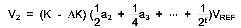
- the D/A converter DAC-1 has a gain of K
- the D/A converter DAC-2 has a gain of K-AK (where AK is a gain error between the DAC-1 and DAC-2).
- n-1 f .
- the gain error appears at each increment of logic input, differently from the conventional accumulation manner using a plurality of D/Aconverters in parallel.
- the amount of error is compressed to 1/2 £ .
- the reason for this is that the amount to be successively and alternatively incremented corresponds to the LSB of each D/A converter and therefore is equal to one step amount which can be obtained by dividing the full scale of the D/A converter output by 2 £ . Therefore, the gain error is also compressed at the same ratio.
- V 1 and V 2 of the DAC-1 and DAC-2 can be expressed as follows: where V REF is a reference potential supplied to DAC-1 and DAC-2.
- an actual half scale output V HS of the combined D/C converter appears when only one of the two D/C converters, for example, DAC-1 is put in the full scale condition.
- the actual half scale output V HF is expressed as follows:
- the ratio L.E. of the combined D/A converter in accordance with the present invention is compressed to 1/2l in comparison to the conventional accumulation method.
- FIG 5 there is shown one embodiment of the A/D converter in accordance with the present invention.
- a voltage V R is applied to the first reference potential terminal 46, and the second reference potential terminal 48 is grounded.
- a voltage V R /2 is applied to the third reference potential terminal 40.
- the capacitor 50 has a capacitance C c of 64C.
- the comparator 36 In case of V IN > V R /2, the comparator 36 will output a logic signal of "1". To the contrary, if V IN ⁇ V R /2, the comparator 36 outputs a logic signal of "0". The logic output of the comparator 36 is applied to the successive approximation register 42, and as a result, the operation will enter the comparison step for the second significant bit (2SB).
- the above operation will be repeated until the comparison for the least significant bit (LSB) is executed.
- the comparison result for the LSB is then inputted to the successive approximation register 42, and so, the content of the register is outputted through the output terminal as the result of the A/D conversion.
- TABLE 2 and TABLE 3 indicate the correspondence between the bit data D 1 ⁇ D 6 and the position of the switches of all the D/A converters which can be taken in the course of the successive approximation operation.
- "1" appearing in the switch position columns indicates that the switch is connected to the first reference potential
- "0" appearing in the switch position columns shows the switch is connected to the second reference potential.
- FIG. 6 there is shown a circuit of the control signal generator44 which can control the switches S 10 ⁇ S 14 , S 20 ⁇ S 24 , S 30 ⁇ S 34 and S 40 ⁇ S44 in accordance with the TABLE 2 and TABLE 3.
- the generator 44 has a 6 bit parallel input for receiving the bit data D 1 ⁇ D 6 of the successive approximation register 42.
- the generator 44 comprises a number of AND gates, OR gates and NOR gates connected as shown to form a decoder which generates logic signals S 10 ⁇ S 44 for control of switches in accordance with the TABLE 2 and the TABLE 3.
- the logic signals S 10 ⁇ 8 44 are at "1"
- the switch is connected to the first reference potential.
- With logic signal of "0" the switch is connected to the second reference potential.
- FIG 7 there is shown another embodiment of the 6 bit A/D converter in accordance with the present invention.
- elements similar to those shown in Figure 5 are given the same Reference Numerals, and explanation will be omitted.
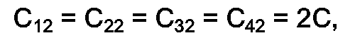
- each of the local D/A converters 34A to 34D has six charge redistribution and sample and hold capacitors C 10 ⁇ C 15 , C 20 ⁇ C 25 , C 30 ⁇ C 35 and C 40 ⁇ C 45 and six associated switches S 10 ⁇ S 15 , S 20 - S 25 , S 30 ⁇ S 35 and S 40 ⁇ S 45 .
- the capacitors of the respective capacitor arrays have capacitances fulfiling the following relation.
- the capacitor 50 has a capacitance of 64C, similarly to the embodiment shown in Figure 5.
- the capacitors incorporated in the local D/A converters has a capacitance of 1C at minimum and a capacitance of 4C at maximum. Therefore, in the case that the A/D converter is fabricated on an integrated circuit, the capacitors can be formed with a high relative precision in capacitance, and therefore, a high A/D conversion accuracy can be obtained.
- TABLE 4 and TABLE 5 indicate the correspondence between the bit data D 1 ⁇ D 6 of the register 42 and the position of the switches S 10 ⁇ S 45 in the case of the second embodiment shown in Figure 7.
- "1" and "2" in the switch position columns have the same meanings as those in TABLE 2 and TABLE 3.
- Figure 8 shows a circuit of the control signal generator 44 for controlling the switches S 10 ⁇ S 15 , S 20 ⁇ S 25 , S 30 ⁇ S 35 and S 40 ⁇ S 45 of the A/D converter shown in Figure 7 in accordance with TABLE 4 and TABLE 5.
- the shown generator includes a number of AND gates, OR gates and NOR gates connected as shown to constitute a decoder which responds to the bit data D i - D 6 of the register 42 so as to generate control signals for all the switchs S 10 ⁇ S 45 in accordance with TABLE 4 and TABLE 5.
- the gain error of each D/Aconverter is uniformly distributed over the range from zero to the full scale. Therefore, a large gain error will not appear as a whole.
- the linearity error can be greatly improved.
Description
- The present invention relates to an analog-to-digital converter, and more specifically to a successive approximation type analog-to-digital converter which includes a plurality of local digital-to-analog converters of a given resolution and which can provide a resolution higher than the given resolution of the digital-to-analog converter.
- GB-A-2 102 227 shows an analog-to-digital-converter of this king having two local DAC's of different size being controlled by a successive approximation register.
- EP-A-0 066 251 shows a local DAC comprising means for dividing the input-digital signal into a plurality of digital signals of smaller bit size than the input signal, a corresponding plurality of DAC's for converting these signals into analog output signals and means for summing the analog output signals to produce a summed analog output signal. Such a local DAC is described in connection with Fig. 4 of the present application.
- At present, digital technique has been widely used in various fields. As a result, analog-to-digital converters (called "A/D converter" hereinafter) and a digital-to-analog converter (called "D/A converter" hereinafter) become very important as an interface between an analog signal and a digital signal.
- Among different types of A/D converters, a successive approximation type A/D converter is known as one which can operate at an intermediate or high speed and can provide a digital signal composed of a relatively large number of bits.
- Referring to Figure 1, there is shown a block diagram of a typical example of a conventional successive approximation type A/D converter. The shown A/D converter includes an analog
signal input terminal 10 connected to a first input of a sample and holdcircuit 12, which has a second input connected to an output of a local D/Aconverter 14. The sample andhold circuit 12 has a pair of outputs corresponding to the pair of inputs, these outputs being connected to a pair of inputs of acomparator 16, whose output is connected to asuccessive approximation register 18. Thisregister 18 has parallel outputs connected to the local D/A converter 14. Further, a serial output of theregister 18 is connected to a digitalsignal output terminal 20. - With this arrangement, the local D/A converter is so set to generate a voltage VFs/2 corresponding to a half of the full scale voltage VFS when it receives the parallel output of the
register 18 composed of the most significant bit (MSB) of "1" and the other bits of "0". In this condition, the voltage of the analog signal held in the sample and holdcircuit 12 is compared with the output voltage VFs/2 of the local D/Aconverter by thecomparator 16. The result of comparison is outputted to thesuccessive approximation register 18, which changes its content, i.e., a digital data to be supplied to the local D/A converter 14. For example, when the input analog signal is larger than VFs/2, the MSB of theregister 18 is maintained at "1" as it is, and the second significant bit (2SB) is changed to "1" from "0". The other bits are maintained at "0". Accordingly, the output voltage of the D/A converter 14 is brought into 3VFs/4. On the other hand, when the input analog signal is smaller that VFs/2, the MSB and 2SB of theregister 18 are changed to "0" and "1", respectively, and the other bits are maintained at "0". In this case, the D/A converter 14 generates VFs/4. Thus, the value of the MSB is determined, and then, the next comparison is made between the input analog signal and the reference voltage VFs/4 or 3VFs/4 of the local D/Aconverter 14, so that the 2SB will be determined. Thus, similar operation will be repeated to successively determine each bit of the digital data until the least significant bit (LSB) is determined. - In the above mentioned successive approximation A/D converter, the local D/Aconverter is generally divided into two types, one of which includes a resistor string or ladder and the other of which includes a capacitor array.
- At present, D/A converters, which have a resolution of 8 bits to 10 bits and which can be used as the local D/
A converter 14 in the above mentioned conventional successive approximation A/D converter, can be manufactured in mass production manner with high reliability and stability in accordance with recent advanced integrated circuit technique. Therefore, A/D converters having a relatively small bit number can be manufactured with reliability. - However, components fabricated on an integrated circuit have a certain limit in uniformity of characteristics, and therefore, it is the present status that it is difficult to obtain a D/A converter having a higher resolution. For example, in order to obtain a D/A converter having a resolution of 12 bits to 16 bits, it is necessary to constitute a circuit with discrete parts such as resistors and capacitors of the accuracy matching with the required resolution. Otherwise, it is necessary to use a fine adjustment means such as a Laser trimming. In this case, however, the cost for forming required elements becomes very large, and also, elements having a sufficient reliability cannot be obtained.
- As mentioned above, in the case that a D/A converter of a large bit number is constituted in combination with a single resistor string or ladder of a single capacitor array, a sufficient accuracy cannot be obtained because the D/A converter cannot maintain a monotonic increase over the full range because of dispersion of element characteristics. For overcoming this problem, there has been proposed to use a plurality of D/A converters in parallel. For example, if two D/A converters are combined in parallel, the combined D/A converter can have a full scale corresponding to the sum of respective full scales of the two unitary D/Aconverters. Assuming that first and second unitary D/Aconverters have full scales FS1 and FS2, respectively, the combined D/A converter has a full scale FS equal to (FS1 + FS2).
- In the combined D/A converter, the first unitary D/A converter will increment its output in response to increment of a digital input. When the MSB of the digital input changes from "0" to "1", the logic value "1" is supplied to all input bits of the first unitary D/A converter so that it outputs its full scale FS1. Thereafter, the second unitary D/Aconverterwill increment in response to increment of the digital input, so that the output of the second D/A converter is added to the output of the first D/A converter to provide a combined output.
- Further, an interpolation type which uses a master D/Aconverter and a slave D/Aconverter has been proposed. In this case, one step of the master D/A converter is divided further finely by the slave D/A converter.
- However, the first mentioned accumulation method using a plurality of unitary D/A converters in parallel is disadvantageous in that a gain error of each unitary D/A converter is accumulated, with the result that the overall D/A converter has a large error in total linearity. On the other hand, the interpolation type has such a defect that it cannot have a monotonic increase if a slave D/A converter has an increased step error.
- Accordingly, it is an object of the present invention to provide an A/D converter which has overcome the above mentioned drawbacks of the conventional ones.
- Another object of the present invention is to provide a successive approximation A/D converter which uses a plurality of D/A converters but which does not have a large gain error as a whole.
- A further object of the present invention is to provide a successive approximation A/D converter which includes a plurality of D/A converters and has an improved linearity error.
- This object of the present invention is solved by the features of
claim 1. - A preferred embodiment is described by the subclaims.
- The above and other objects, features and advantages of the present invention will be apparent from the following description of preferred embodiments of the invention with reference to the accompanying drawings.
-
- Figure 1 is a block diagram showing one example of the conventional successive approximation A/D converter;
- Figure 2 is a block diagram showing a basic construction of the successive approximation A/D converter in accordance with the present invention;
- Figure 3 is a more detailed block diagram of the A/D converter shown in Figure 2;
- Figure 4 is a diagram illustrating a basic conception of the A/D converter shown in Figure 2;
- Figure 5 is a diagram similar to Figure 3 but showing a first embodiment of the successive approximation A/D converter in accordance with the present invention;
- Figure 6 is a circuit diagram of a switch control signal generator incorporated in the A/D converter shown in Figure 5;
- Figure 7 is a diagram similar to Figure 3 but showing a second embodiment of the successive approximation A/D converter; and
- Figure 8 is a diagram similar to Figure 6 but showing a switch control signal generator incorporated in the A/D converter shown in Figure 7.
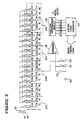
- Referring to Figure 2, there is shown a conceptual structure of the successive approximation A/D converter in accordance with the present invention. The shown A/D converter includes an analog
signal input terminal 30 connected to an analogsignal input circuit 32. Thisinput circuit 32 has an output connected commonly to a plurality of local D/A converters 34A to 34K of the charge redistribution type which has a capacitor array functioning a charge redistribution and sample and hold capacitor for the first bit to the bit of 2m. These local D/A converter has a resolution off" bits. Outputs of all the D/A converters 34A to 34K are connected commonly to one input of thecomparator 36. - This
comparator 36 has another input connected to acapacitor 38, which is in turn connected to a referencepotential terminal 40. Thecomparator 36 is connected at its output to asuccessive approximation register 42. Thisregister 42 has parallel outputs connected to agenerator 44 which supplies switch control signals to all the local D/A converters 34A to 34K so as to cause the respective D/A converters to change their internal condition. Further, theregister 42 is adapted to output an digital signal of n bits. In this construction, the relation of n = f + m and K = 2 m is established. - With this arrangement, an analog signal is supplied from the
input terminal 30 through theinput circuit 32 to all the first to the kth local D/A converters 34A to 34K. Specifically, the analog signal is sampled in the ca- pacitorarray of each D/Aconverters controlled by the control signal generator44. Then, the analogsignal input circuit 32 is cut off so that the analog signal is held in the respective capacitor array. Thereafter, comparison between the outputs of all the D/A converters and the reference potential is made by thecomparator 36, and the content of theregister 42 is modified on the basis of the comparison result. In response to the content of theregister 42, thegenerator 44 generates such control signals to the D/Aconverters 34A to 34K that the condition of the capacitor arrays is successively modified one by one comparison. Thus, a digital signal of n bits is finally outputted from theregister 42. - Turning to Figure 3, the
register 42 has parallel bit outputs supplying n-bit data D1, D2, D3··· Dn-1 and Dn to thegenerator 44. On the other hand, the first D/A converter 34A includes a capacitor array composed of (f + 1) capacitors C10 to C1ℓ which function as a charge redistribution and sample and hold capacitor. One electrodes of these capacitors C10 to C1ℓ are connected to each other. The other electrode of each capacitor C10 to C1ℓ is connected to a common terminal of a single pole triple throws switch S10 to S1ℓ. Each of the switches S10 to S1ℓ has a first selection terminal connected to the analogsignal input terminal 30, a second selection terminal connected to a first referencepotential terminal 46, and a third selection terminal connected to a second referencepotential terminal 48. Similarly, the second D/A converter 34B includes a capacitor array of (f + 1) capacitors C20 to C2c and associated switches S20 to S2C connected as shown. Further, the other D/A converters each includes (f + 1) capacitors and (f + 1) associated switches. The commonly connected electrodes of the capacitors of each D/A converters 34A to 34K are also connected commonly to one input of thecomparator 36. - The other input of the
comparator 36 is connected through acapacitor 50 to a third referencepotential terminal 40. Thecapacitor 50 is shunted by aswitch 52, and the third referencepotential terminal 40 is connected through anotherswitch 34 to the one input of thecomparator 36. - The above capacitors are in the following relation: The
capacitor 50 has a capacitance Cc equal to the total capacitance of all capacitors C10 ~ C1f, C20 ~ C2ℓ, ... Cko ~ CkC included in all the D/A converters 34A to 34K. Further, assuming that a unitary capacitance is C, the capacitors C10 ~ C1f, C20 ~ C2ℓ, ... , Cko ~ CkC of each of the first to Kth D/A converters 34A to 34K are weighted to have capacitances C, C, 2C, ... , and 2(ℓ- 1)C respectively. Therefore, Cc = (K x 2ℓ)C. - Before explaining the operation of the embodiment, description will be made on operation of a combined D/A converter which receive n bit data and which includes two (n-1) bit D/A converters, with references to Figure 4.
- The n bit data DATA-A is divided into a portion of only LSB (the nth bit) and a portion of (n-1)th bit to MSB. The latter portion is supplied as a (n-1) bit data DATA-B to one D/A converter DAC-2, and also inputted to a digital adder ADD-1. This adder adds the LSB of DATA-A to the LSB of DATA-B (i.e., the (n-1)th bit of DATA-A) and supplies the result of addition as another (n-1) bit data DATA-C to another D/Aconverter DAC-1. Outputs of the two D/Aconverters DAC-1 and DAC-2 are inputted to an analog adderADD-2 which generates an analog signal corresponding to the input digital signal DATA-A.
- Now, assuming n = 6, the digital data DATA-A, DATA-B and DATA-C are under the relation shown in the following TABLE-1.

- As seen from the above TABLE-1, the (n-1) bit digital inputs to the D/A converters DAC-1 and DAC-2 are alternatively and successively incremented dependently upon the LSB of the input digital data.
- Now, assume that the D/A converter DAC-1 has a gain of K, and the D/A converter DAC-2 has a gain of K-AK (where AK is a gain error between the DAC-1 and DAC-2). Further, assume n-1 =f . Under this condition, the gain error appears at each increment of logic input, differently from the conventional accumulation manner using a plurality of D/Aconverters in parallel. However, the amount of error is compressed to 1/2£ . The reason for this is that the amount to be successively and alternatively incremented corresponds to the LSB of each D/A converter and therefore is equal to one step amount which can be obtained by dividing the full scale of the D/A converter output by 2£. Therefore, the gain error is also compressed at the same ratio.
- Reviewing in detail, the outputs V1 and V2 of the DAC-1 and DAC-2 can be expressed as follows:

- Therefore, in the conventional accumulation method, the full scale output VFS is

- Thus, an ideal half scale output of the combined D/C converter is expressed:

- On the other hand, an actual half scale output VHS of the combined D/C converter appears when only one of the two D/C converters, for example, DAC-1 is put in the full scale condition. The actual half scale output VHF is expressed as follows:

- Accordingly, the linearity error VLE(HS) in the half scale is expressed:

- The ratio L.E. Of VLE(HS) to the full scale is as follows:

- On the other hand, the full scale voltage VFS in the combined D/Aconvertershown in Figure 4 is expressed as follows:

- Namely, this is similar to that of the conventional accumulation method. Further, the magnitude of change VSTEP caused by the LSBs of the DAC-1 and DAC-2 is expressed;


- The linearity error due to the gain error will therefore appear at every two steps over the whole of the dynamic range. But, the magnitude of the error is compressed.
- As ideal neutral point potential of the two steps can be expressed:


- As seen from the above, the ratio L.E. of the combined D/A converter in accordance with the present invention is compressed to 1/2ℓ in comparison to the conventional accumulation method.
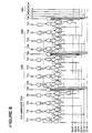
- Referring to Figure 5, there is shown one embodiment of the A/D converter in accordance with the present invention. In Figure 4, elements similar to those shown in Figure 3 are given the same Reference Numerals, and explanation will be omitted. For simplification of drawing and explanation, the shown A/D converter is adapted to output a 6 bit digital signal. Namely, n = 6. Further, the shown converter is constructed on the condition of f = 4, m = 2 and K = 22 = 4. In the first embodiment shown in Figure 5, further, a voltage VR is applied to the first reference
potential terminal 46, and the second referencepotential terminal 48 is grounded. In addition, a voltage VR/2 is applied to the third referencepotential terminal 40. Under these conditions, four local D/A converters 


capacitor 50 has a capacitance Cc of 64C. - Next, an A/D conversion operation will be explained. First, all the switches S10 ~ S14, S20 ~ S24, S30 ~ S34 and S40 ~ S44 are controlled to connect the
analog signal input 30, and theswitches input 30 is sampled in all the capacitor arrays of the D/Aconverters 34A to 34D in comparison to the third reference potential VR/2. - Next, the
switches approximate register 42 is changed to such a condition that D1 "1" and D2 ~ D6 = "0". As a result, all the switches S10 ~ S14, S20 ~ S24, S30 ~ S34, S40 ~ S44 are separated from theanalog signal input 30. In addition, since the bit data D1 is brought to "1", all the switches S14, S24, S34 and S44 connected to the capacitors C14, C24, C34 and C44 of thecapacitance 8C are connected to the first referencepotential terminal 46 of the potential VR. Since the other bit data D2 to D6 are kept at "0", the other switches S10 ~ S13, S20 ~ S23, S30 ~ S33 and S40 ~ S43 are connected to the second referencepotential terminal 48 of the ground level. In this condition, comparison is made by thecomparator 36. Namely, there has been performed a comparison step for the most significant bit (MSB) in the successive approximation system. - Now, assuming that the respective potentials of the inverted input and the non-inverted input of the
comparator 36 are VI and VN, respectively, the following relation can be formed:


- In case of VIN > VR/2, the
comparator 36 will output a logic signal of "1". To the contrary, if VIN < VR/2, thecomparator 36 outputs a logic signal of "0". The logic output of thecomparator 36 is applied to thesuccessive approximation register 42, and as a result, the operation will enter the comparison step for the second significant bit (2SB). Specifically, with VIN > VR/2, the bit data D1 and D2 are put at "1" and the other bit data D3 to D6 are put at "0", with the result that the switches S13, S14, S24, S34 and S44 are connected to the first reference potential V R, and the other switches S10 ~ S12, S20 ~ S23, S30 ~ S33 and S40 ~ S43 are connected to the second reference potential of the ground level. In this condition, the following relation is established:


- As a result, if VIN > 3VR/4, the
comparator 36 outputs a signal of "1". On the other hand, if VIN < 3VR/4, thecomparator 36 generates a signal of "0". The output of thecomparator 36 is applied to thesuccessive approximation register 42. - The above operation will be repeated until the comparison for the least significant bit (LSB) is executed. The comparison result for the LSB is then inputted to the
successive approximation register 42, and so, the content of the register is outputted through the output terminal as the result of the A/D conversion. - The following TABLE 2 and TABLE 3 indicate the correspondence between the bit data D1 ~ D6 and the position of the switches of all the D/A converters which can be taken in the course of the successive approximation operation. In these tables, "1" appearing in the switch position columns indicates that the switch is connected to the first reference potential, and "0" appearing in the switch position columns shows the switch is connected to the second reference potential.


- Turning to Figure 6, there is shown a circuit of the control signal generator44 which can control the switches S10 ~ S14, S20 ~ S24, S30 ~ S34 and S40 ~ S44 in accordance with the TABLE 2 and TABLE 3. The
generator 44 has a 6 bit parallel input for receiving the bit data D1 ~ D6 of thesuccessive approximation register 42. Thegenerator 44 comprises a number of AND gates, OR gates and NOR gates connected as shown to form a decoder which generates logic signals S10 ~ S44 for control of switches in accordance with the TABLE 2 and the TABLE 3. When the logic signals S10 ~ 844 are at "1", the switch is connected to the first reference potential. On the other hand, with logic signal of "0", the switch is connected to the second reference potential. - Referring to Figure 7, there is shown another embodiment of the 6 bit A/D converter in accordance with the present invention. In this figure, elements similar to those shown in Figure 5 are given the same Reference Numerals, and explanation will be omitted.
- In this embodiment, each of the local D/
A converters 34A to 34D has six charge redistribution and sample and hold capacitors C10 ~ C15, C20 ~ C25, C30 ~ C35 and C40 ~ C45 and six associated switches S10 ~ S15, S20 - S25, S30 ~ S35 and S40 ~ S45. The capacitors of the respective capacitor arrays have capacitances fulfiling the following relation.

- Therefore, the
capacitor 50 has a capacitance of 64C, similarly to the embodiment shown in Figure 5. - In the second embodiment shown in Figure 7, the capacitors incorporated in the local D/A converters has a capacitance of 1C at minimum and a capacitance of 4C at maximum. Therefore, in the case that the A/D converter is fabricated on an integrated circuit, the capacitors can be formed with a high relative precision in capacitance, and therefore, a high A/D conversion accuracy can be obtained.
- The following TABLE 4 and TABLE 5 indicate the correspondence between the bit data D1 ~ D6 of the
register 42 and the position of the switches S10 ~ S45 in the case of the second embodiment shown in Figure 7. "1" and "2" in the switch position columns have the same meanings as those in TABLE 2 and TABLE 3.

- Figure 8 shows a circuit of the
control signal generator 44 for controlling the switches S10 ~ S15, S20 ~ S25, S30 ~ S35 and S40 ~ S45 of the A/D converter shown in Figure 7 in accordance with TABLE 4 and TABLE 5. Namely, the shown generator includes a number of AND gates, OR gates and NOR gates connected as shown to constitute a decoder which responds to the bit data Di - D6 of theregister 42 so as to generate control signals for all the switchs S10 ~ S45 in accordance with TABLE 4 and TABLE 5. - As will be apparent from the above description of the embodiments with the reference to the drawings, a n-bit successive approximation A/D converter can be constructed by using 2m f-bit local D/A converters (where f < n, and n = f + m) in parallel so as to form a combined D/A converter, and by successively and alternatively incrementing the 2m D/A converters so that the combined analog output is incremented. With the arrangement, the gain error of each D/Aconverter is uniformly distributed over the range from zero to the full scale. Therefore, a large gain error will not appear as a whole. In addition, the linearity error can be greatly improved.
- Further, since there are used a plurality of D/A converter of the bit number smaller than a desired bit number, when the A/D converter is fabricated on an integrated circuit, it is possible to suppress an adverse effect of dispersion in characteristics of components formed on the integrated circuit.
- The invention has thus been shown and described with reference to the specific embodiments. However, it should be noted that the invention is in no way limited to the details of the illustrated structures but changes and modifications may be made within the scope of the appended claims.
Claims (3)
Applications Claiming Priority (2)
| Application Number | Priority Date | Filing Date | Title |
|---|---|---|---|
| JP144364/86 | 1986-06-19 | ||
| JP61144364A JPH0761019B2 (en) | 1986-06-19 | 1986-06-19 | Analog to digital converter |
Publications (3)
| Publication Number | Publication Date |
|---|---|
| EP0249986A2 EP0249986A2 (en) | 1987-12-23 |
| EP0249986A3 EP0249986A3 (en) | 1991-07-03 |
| EP0249986B1 true EP0249986B1 (en) | 1995-12-20 |
Family
ID=15360388
Family Applications (1)
| Application Number | Title | Priority Date | Filing Date |
|---|---|---|---|
| EP87108802A Expired - Lifetime EP0249986B1 (en) | 1986-06-19 | 1987-06-19 | Analog-to-digital converter |
Country Status (4)
| Country | Link |
|---|---|
| US (1) | US4764750A (en) |
| EP (1) | EP0249986B1 (en) |
| JP (1) | JPH0761019B2 (en) |
| DE (1) | DE3751639T2 (en) |
Families Citing this family (31)
| Publication number | Priority date | Publication date | Assignee | Title |
|---|---|---|---|---|
| JPH0734541B2 (en) * | 1987-07-27 | 1995-04-12 | 日本電気株式会社 | Successive approximation type analog-digital conversion system |
| US5377248A (en) * | 1988-11-29 | 1994-12-27 | Brooks; David R. | Successive-approximation register |
| AU640354B2 (en) * | 1988-11-29 | 1993-08-26 | Magellan Corporation (Australia) Pty Ltd | Successive-approximation register |
| US5047665A (en) * | 1989-02-08 | 1991-09-10 | Burr-Brown Corporation | Low noise, low offset, high speed CMOS differential amplifier |
| US4940981A (en) * | 1989-02-08 | 1990-07-10 | Burr-Brown Corporation | Dual analog-to-digital converter with single successive approximation register |
| IT1229752B (en) * | 1989-05-17 | 1991-09-10 | Sgs Thomson Microelectronics | HIGH SPEED ANALOG / DIGITAL CONVERTER. |
| US5272481A (en) * | 1991-07-02 | 1993-12-21 | David Sarnoff Research Center, Inc. | Successive approximation analog to digital converter employing plural feedback digital to analog converters |
| US5172019A (en) * | 1992-01-17 | 1992-12-15 | Burr-Brown Corporation | Bootstrapped FET sampling switch |
| JPH05343998A (en) * | 1992-06-10 | 1993-12-24 | Mitsubishi Electric Corp | Sequential converting type a/d converter |
| US5367302A (en) * | 1993-08-24 | 1994-11-22 | Burr-Brown Corporation | Isolating a CDAC array in a current integrating ADC |
| US5471208A (en) * | 1994-05-20 | 1995-11-28 | David Sarnoff Research Center, Inc. | Reference ladder auto-calibration circuit for an analog to digital converter |
| US5604501A (en) * | 1994-10-21 | 1997-02-18 | Lucent Technologies Inc. | Digital-to-analog converter with reduced number of resistors |
| US5619203A (en) * | 1994-10-21 | 1997-04-08 | Lucent Technologies Inc. | Current source driven converter |
| US6259392B1 (en) * | 1997-10-08 | 2001-07-10 | Samsung Electronics Co., Ltd. | Multiplying digital-to-analog converters and methods that selectively connect unit and feedback capacitors to reference voltages and feedback voltages |
| US6215428B1 (en) * | 1997-10-14 | 2001-04-10 | Photobit Corporation | Differential non-linearity correction scheme |
| US6587066B1 (en) * | 2002-01-18 | 2003-07-01 | Cirrus Logic, Inc. | Circuits and methods for sampling an input signal in a charge redistribution digital to analog converter |
| FI20020324A0 (en) * | 2002-02-18 | 2002-02-18 | Ari Paasio | Analog-to-digital converter, power scaler and method to control power scaler function |
| DE10303347B4 (en) * | 2003-01-29 | 2010-04-29 | Eads Deutschland Gmbh | Method and circuit for converting an analog actual signal into a digital desired signal |
| DE50303186D1 (en) * | 2003-02-05 | 2006-06-08 | Alcatel Sa | Method for digital-to-analog conversion and digital-to-analog converter |
| DE10307007B3 (en) * | 2003-02-19 | 2004-07-29 | Siemens Ag | Evaluation method for capacitive sensor e.g. for automobile tyre pressure sensor, using comparison of sensor actual value with comparison capacitance provided by switched partial capacitances |
| US8065022B2 (en) * | 2005-09-06 | 2011-11-22 | General Electric Company | Methods and systems for neural network modeling of turbine components |
| JP5287291B2 (en) | 2009-01-26 | 2013-09-11 | 富士通セミコンダクター株式会社 | Successive comparison type A / D converter |
| JP5440758B2 (en) * | 2009-05-07 | 2014-03-12 | セイコーエプソン株式会社 | A / D conversion circuit, electronic device, and A / D conversion method |
| US8244927B2 (en) | 2009-10-27 | 2012-08-14 | Fairchild Semiconductor Corporation | Method of detecting accessories on an audio jack |
| US8004448B2 (en) * | 2009-11-16 | 2011-08-23 | Analog Devices, Inc. | Dual DAC structure for charge redistributed ADC |
| US8004441B1 (en) * | 2010-03-18 | 2011-08-23 | International Business Machines Corporation | Small-area digital to analog converter based on master-slave configuration |
| US9229833B2 (en) * | 2011-01-28 | 2016-01-05 | Fairchild Semiconductor Corporation | Successive approximation resistor detection |
| US9060228B2 (en) | 2012-08-03 | 2015-06-16 | Fairchild Semiconductor Corporation | Accessory detection circuit with improved functionality |
| US9391632B1 (en) * | 2015-01-27 | 2016-07-12 | Omnivision Technologies, Inc. | Method and system for implementing an extended range approximation analog-to-digital converter |
| JP6703814B2 (en) * | 2015-08-28 | 2020-06-03 | ルネサスエレクトロニクス株式会社 | AD converter and AD converter |
| KR20220045455A (en) * | 2020-10-05 | 2022-04-12 | 에스케이하이닉스 주식회사 | Analog-digital converter, memory device and operating method including the same |
Citations (1)
| Publication number | Priority date | Publication date | Assignee | Title |
|---|---|---|---|---|
| US4195282A (en) * | 1978-02-01 | 1980-03-25 | Gte Laboratories Incorporated | Charge redistribution circuits |
Family Cites Families (6)
| Publication number | Priority date | Publication date | Assignee | Title |
|---|---|---|---|---|
| FR2357110A1 (en) * | 1976-07-01 | 1978-01-27 | Trt Telecom Radio Electr | D=A converter system - uses two channels with converters providing max. accuracy in middle of scale |
| US4318085A (en) * | 1978-06-01 | 1982-03-02 | The Bendix Corporation | Method and apparatus for conversion of signal information between analog and digital forms |
| US4412208A (en) * | 1980-09-16 | 1983-10-25 | Nippon Telegraph & Telephone Public Corporation | Digital to analog converter |
| JPS57194625A (en) * | 1981-05-27 | 1982-11-30 | Nec Corp | Digital to analog converter |
| JPS5810919A (en) * | 1981-07-13 | 1983-01-21 | Nippon Telegr & Teleph Corp <Ntt> | Analog-to-digital converter |
| US4476456A (en) * | 1981-11-03 | 1984-10-09 | Texas Instruments Incorporated | Combination of an analog to digital converter and sampling switch |
-
1986
- 1986-06-19 JP JP61144364A patent/JPH0761019B2/en not_active Expired - Lifetime
-
1987
- 1987-06-19 DE DE3751639T patent/DE3751639T2/en not_active Expired - Lifetime
- 1987-06-19 EP EP87108802A patent/EP0249986B1/en not_active Expired - Lifetime
- 1987-06-19 US US07/063,896 patent/US4764750A/en not_active Expired - Lifetime
Patent Citations (1)
| Publication number | Priority date | Publication date | Assignee | Title |
|---|---|---|---|---|
| US4195282A (en) * | 1978-02-01 | 1980-03-25 | Gte Laboratories Incorporated | Charge redistribution circuits |
Also Published As
| Publication number | Publication date |
|---|---|
| EP0249986A2 (en) | 1987-12-23 |
| JPH0761019B2 (en) | 1995-06-28 |
| DE3751639T2 (en) | 1996-09-05 |
| DE3751639D1 (en) | 1996-02-01 |
| US4764750A (en) | 1988-08-16 |
| EP0249986A3 (en) | 1991-07-03 |
| JPS631120A (en) | 1988-01-06 |
Similar Documents
| Publication | Publication Date | Title |
|---|---|---|
| EP0249986B1 (en) | Analog-to-digital converter | |
| US4638303A (en) | Digital-analog converter | |
| US5012247A (en) | Switched-capacitor analog-to-digital converter with autocalibration | |
| JP3253901B2 (en) | Digital / analog converter | |
| US6600437B1 (en) | High resolution, high speed, low power switched capacitor digital to analog converter | |
| US4316178A (en) | Digital-to-analog conversion system with compensation circuit | |
| US4831381A (en) | Charge redistribution A/D converter with reduced small signal error | |
| JP3115296B2 (en) | Self-calibrating AD and DA converter | |
| US5426431A (en) | Analog/digital converter | |
| EP0130466A2 (en) | A capacitive digital to analog converter which can be trimmed | |
| EP0075441B1 (en) | Voltage dividing circuit | |
| US4388612A (en) | Signal converter | |
| JP3857450B2 (en) | Successive comparison type analog-digital conversion circuit | |
| US4947172A (en) | Digital-to-analog conversion circuit | |
| EP0289081B1 (en) | Digital-to-analog converter | |
| CN115099182B (en) | Integral design method for segmented CDAC (capacitor-to-capacitor converter) bridge capacitor and analog-to-digital converter | |
| US6259392B1 (en) | Multiplying digital-to-analog converters and methods that selectively connect unit and feedback capacitors to reference voltages and feedback voltages | |
| US5173698A (en) | Flash analog-to-digital converter with integrating input stage | |
| JP2837726B2 (en) | Digital to analog converter | |
| JPH0262123A (en) | Serial/parallel type a/d converter | |
| EP0251758A2 (en) | Digital-to-analog conversion system | |
| EP0681372B1 (en) | Digital-to-analog conversion circuit and analog-to-digital conversion device using the circuit | |
| JPH05268093A (en) | Digital/analog converter | |
| EP0247065B1 (en) | An untrimmed 12 bit monotonic all capacitive a to d converter | |
| JP3130007B2 (en) | Successive approximation type A / D converter circuit |
Legal Events
| Date | Code | Title | Description |
|---|---|---|---|
| PUAI | Public reference made under article 153(3) epc to a published international application that has entered the european phase |
Free format text: ORIGINAL CODE: 0009012 |
|
| 17P | Request for examination filed |
Effective date: 19870715 |
|
| AK | Designated contracting states |
Kind code of ref document: A2 Designated state(s): DE FR GB |
|
| PUAL | Search report despatched |
Free format text: ORIGINAL CODE: 0009013 |
|
| AK | Designated contracting states |
Kind code of ref document: A3 Designated state(s): DE FR GB |
|
| 17Q | First examination report despatched |
Effective date: 19920818 |
|
| GRAA | (expected) grant |
Free format text: ORIGINAL CODE: 0009210 |
|
| AK | Designated contracting states |
Kind code of ref document: B1 Designated state(s): DE FR GB |
|
| REF | Corresponds to: |
Ref document number: 3751639 Country of ref document: DE Date of ref document: 19960201 |
|
| ET | Fr: translation filed | ||
| PLBE | No opposition filed within time limit |
Free format text: ORIGINAL CODE: 0009261 |
|
| STAA | Information on the status of an ep patent application or granted ep patent |
Free format text: STATUS: NO OPPOSITION FILED WITHIN TIME LIMIT |
|
| 26N | No opposition filed | ||
| REG | Reference to a national code |
Ref country code: GB Ref legal event code: IF02 |
|
| REG | Reference to a national code |
Ref country code: GB Ref legal event code: 732E |
|
| REG | Reference to a national code |
Ref country code: FR Ref legal event code: TP |
|
| APAH | Appeal reference modified |
Free format text: ORIGINAL CODE: EPIDOSCREFNO |
|
| PGFP | Annual fee paid to national office [announced via postgrant information from national office to epo] |
Ref country code: FR Payment date: 20060608 Year of fee payment: 20 |
|
| PGFP | Annual fee paid to national office [announced via postgrant information from national office to epo] |
Ref country code: GB Payment date: 20060614 Year of fee payment: 20 |
|
| PGFP | Annual fee paid to national office [announced via postgrant information from national office to epo] |
Ref country code: DE Payment date: 20060615 Year of fee payment: 20 |
|
| REG | Reference to a national code |
Ref country code: GB Ref legal event code: PE20 |
|
| PG25 | Lapsed in a contracting state [announced via postgrant information from national office to epo] |
Ref country code: GB Free format text: LAPSE BECAUSE OF EXPIRATION OF PROTECTION Effective date: 20070618 |