EP0250976A1 - Arrangement for image data processing - Google Patents
Arrangement for image data processing Download PDFInfo
- Publication number
- EP0250976A1 EP0250976A1 EP87108479A EP87108479A EP0250976A1 EP 0250976 A1 EP0250976 A1 EP 0250976A1 EP 87108479 A EP87108479 A EP 87108479A EP 87108479 A EP87108479 A EP 87108479A EP 0250976 A1 EP0250976 A1 EP 0250976A1
- Authority
- EP
- European Patent Office
- Prior art keywords
- address
- memory
- counter
- image
- counters
- Prior art date
- Legal status (The legal status is an assumption and is not a legal conclusion. Google has not performed a legal analysis and makes no representation as to the accuracy of the status listed.)
- Ceased
Links
Images


Classifications
-
- G—PHYSICS
- G06—COMPUTING; CALCULATING OR COUNTING
- G06F—ELECTRIC DIGITAL DATA PROCESSING
- G06F7/00—Methods or arrangements for processing data by operating upon the order or content of the data handled
- G06F7/76—Arrangements for rearranging, permuting or selecting data according to predetermined rules, independently of the content of the data
- G06F7/78—Arrangements for rearranging, permuting or selecting data according to predetermined rules, independently of the content of the data for changing the order of data flow, e.g. matrix transposition or LIFO buffers; Overflow or underflow handling therefor
- G06F7/785—Arrangements for rearranging, permuting or selecting data according to predetermined rules, independently of the content of the data for changing the order of data flow, e.g. matrix transposition or LIFO buffers; Overflow or underflow handling therefor having a sequence of storage locations each being individually accessible for both enqueue and dequeue operations, e.g. using a RAM
-
- G—PHYSICS
- G06—COMPUTING; CALCULATING OR COUNTING
- G06F—ELECTRIC DIGITAL DATA PROCESSING
- G06F16/00—Information retrieval; Database structures therefor; File system structures therefor
- G06F16/50—Information retrieval; Database structures therefor; File system structures therefor of still image data
- G06F16/51—Indexing; Data structures therefor; Storage structures
-
- G—PHYSICS
- G06—COMPUTING; CALCULATING OR COUNTING
- G06T—IMAGE DATA PROCESSING OR GENERATION, IN GENERAL
- G06T1/00—General purpose image data processing
- G06T1/20—Processor architectures; Processor configuration, e.g. pipelining
-
- G—PHYSICS
- G09—EDUCATION; CRYPTOGRAPHY; DISPLAY; ADVERTISING; SEALS
- G09G—ARRANGEMENTS OR CIRCUITS FOR CONTROL OF INDICATING DEVICES USING STATIC MEANS TO PRESENT VARIABLE INFORMATION
- G09G5/00—Control arrangements or circuits for visual indicators common to cathode-ray tube indicators and other visual indicators
- G09G5/36—Control arrangements or circuits for visual indicators common to cathode-ray tube indicators and other visual indicators characterised by the display of a graphic pattern, e.g. using an all-points-addressable [APA] memory
- G09G5/39—Control of the bit-mapped memory
- G09G5/395—Arrangements specially adapted for transferring the contents of the bit-mapped memory to the screen
-
- G—PHYSICS
- G11—INFORMATION STORAGE
- G11C—STATIC STORES
- G11C8/00—Arrangements for selecting an address in a digital store
- G11C8/04—Arrangements for selecting an address in a digital store using a sequential addressing device, e.g. shift register, counter
Definitions
- the invention relates to an arrangement for processing image data according to the preamble of claim 1.
- Such an arrangement is known from the magazines “Elektronik” 1985, number 5, pages 93 and 94 and "Der Elektroniker” 1985, number 1, pages 59 to 67 .
- the known arrangements contain a plurality of processors which process the image data supplied by a camera or read out from an image memory. As long as the image data is read from the memory in the same order as it was written, there are no problems. It is different, however, if the order is to be changed and each address has to be laboriously calculated using software.
- the present invention has for its object to provide an arrangement of the type specified in the preamble of claim 1, with which the data entered in an image memory can be read quickly, even with the pixel frequency, in a changed order.
- this object is achieved with the measures specified in the characterizing parts of claims 1 and 4.
- the solution according to claim 1 it is achieved that when the read image data is displayed on a display device, the displayed image is rotated by ⁇ 90 ° or 180 ° with respect to the original and is additionally mirrored. If the meters are connected in parallel, a diagonal scan takes place.
- the solution according to claim 4 allows the image data to be read out in any order without stressing the process.
- KA designates a television camera to which an analog-to-digital converter ADU is connected, which converts the analog video signals from the camera into digital signals.
- ADU analog-to-digital converter
- DB1 bus line to which two image memories BSP1, BSP2 and a monitor MO are connected.
- Each image memory is connected to a processor PR1, PR2, of which the processor PR2 is used primarily for image evaluation, while the processor PR1 preprocesses the data contained in the image memory BSP1.
- the main memory of the processor is called ASP.
- An addressing unit is connected between the processor PR1 and the image memory BSP1, which, parameterized by the processor PR1, generates the addresses for the image memory BSP1.
- a comparator VGL which is connected to the bus line and which generates binary image data from the image data by comparison with a threshold value or by comparison of two successive image data, which are entered into one of the image memories BSP1, BSP2 via a bus line DB2 can.
- the in the image memories Data contained and the output signals of the ADU analog-digital converter can be displayed with the monitor MO.
- the first image memory is again designated with BSP1.
- the addresses are supplied to it as two partial addresses, the first of which are formed in a first address counter AZ1 and the second in a second address counter AZ2.
- These counters are presettable bidirectional counters.
- a counter control ZST not only controls the counting directions, but also indicates whether the counters are connected in parallel or in series and in what order they are in series. It receives the information about this from the processor PR1 via a register REG1.
- the data inputs and outputs of the image memory BSP1 are connected to a bus line DB3, to which the processor PR1 is also connected via a register REG2.
- the image data can also be transmitted to the monitor MO via this bus line.
- the bus line DB3 is also connected to the lines DB1, DB2 via register REG3, REG4.
- FIG. 3 shows details of the counter control ZST shown in FIG. 2 only as a block.
- the register PR1 is used by processor PR1 to enter the starting counter values for address counters AZ1, AZ2 from its working memory cells FF00, FF01 (see FIG. 1).
- the counting mode is then written into the control register STR from the working memory cell FF10. This is fed as a partial address to a read-only memory PROM. This partial address is completed with the carry pulses of the counters AZ1, AZ2.
- the control inputs VR for upward and downward counting of the counters AZ1, AZ2 are connected to the outputs of the read-only memory PROM.
- Two further outputs of the read-only memory PROM are routed to two OR gates OR1, OR2, to which the enable inputs FR of the counters AZ1, AZ2 connect are closed. Either the counter AZ1 or the counter AZ2 can thus be used, or both counters can be released simultaneously for counting trigger pulses T.
- the trigger pulses can either have a pixel frequency, so that the video signals from the camera KA (FIG. 1) can be entered directly into the image memory BSP1, or the data contained in the image memory BSP1 can be displayed on the display device MO operating according to the line screening method.
- the trigger pulses T are formed each time the processor accesses the image memory BSP1.
- Two switches SC1, SC2 are controlled with two further output signals from the read-only memory PROM.
- the carry pulses of the address counter AZ1 can be fed via the OR gate OR2 to the enable input FR of the address counter AZ2.
- This counter is therefore connected downstream of the counter AZ1 when the switch SC1 is closed.
- switch SC2 is closed, the carry pulses of counter AZ2 are fed to the enable input of counter AZ1. If both switches are open, the two counters work independently of one another, provided that there is no coupling via the PROM read-only memory.
- the number of pixels per line in the measuring field of an image is equal to the number of lines in the measuring field.
- the capacity of the address counters AZ1, AZ2 is equal to the number of pixels per line or the number of lines in the measuring field.
- the switch SC1 is closed, both counters are set to zero before writing, and a trigger pulse is generated for each pixel in the measuring field, the trigger pulse frequency being equal to the pixel frequency.
- the status of the address counter AZ1 indicates the column of the respective scanned pixel and the counter AZ2 is the line that is being scanned. If you view the image memory as two-dimensional, then an image of the captured image is entered in it.
- This image is read out unchanged and displayed on the monitor when the counters AZ1, AZ2 are operated in the same way as when the image is written, ie when the switch SC1 is closed, the enable AZ1 is constantly supplied with an enable signal and both counters are counting upwards are set.
- the read-out image can be changed in different ways compared to the original image, namely that it can be rotated by ⁇ 90 ° or 180 °, it can be on a straight line running in the line direction, a straight line running perpendicular thereto or also on the image diagonals are mirrored and displayed accordingly.
- a diagonal scanning of the image and the evaluation of the image data pre-processed in this way are also possible.
- the image is rotated by + 90 ° if the counter AZ1 is connected after the counter AZ2 and the counter AZ2 is set to count down.
- the counter AZ1 is counted backwards for reflection on the horizontal straight line running through the middle of the picture.
- both counters receive the trigger pulses at the same time.
- the counting mode is changed.
- the carry pulses are fed to the read-only memory PROM, which then outputs the new counting mode.
- the counters can be set to count up or down.
- the processor PR1 accesses the image memory BSP1 in such a way that the desired counting mode is entered in the cell FF02 and this cell is addressed.
- the counting mode is then transferred to the control register STR.
- the content of the addressed cell of the memory BSP1 is entered into the main memory ASP of the processor PR1 and can be compared there with other image data.
- there is a new access to cell FF02 with the same counting mode or a new counting mode is selected be it that this was previously entered in cell FF02 or that a memory cell is provided for each counting mode, e.g. B. cells 03, 04 ... and the cell can be called with the desired mode. In this way you can z. B.
- the image data read from the image memory BSP1 can also be transferred to the image memory BSP2 for further evaluation using the processor PR2.
- the scanning of the image contained in the memory BSP1 in different directions then represents a rapid preprocessing of the image data.
- the arrangement described so far is characterized by its simplicity.
- the image data can also be read out from the memory BSP1 at a high frequency in different orders. However, the order of reading is limited by the number of counting modes.
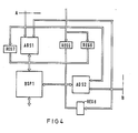
- a freely selectable sequence of the read image data can be achieved with a circuit supplement, the block diagram of which is shown in FIG. 4.
- This circuit is inserted at the locations marked A and B in FIG. It essentially consists of two address memories ADS1, ADS2, which are addressed with the respective states of the counters AZ1, AZ2 and to whose data outputs the address inputs of the image memory BSP1 are connected.
- the address memories ADS1, ADS2 are random memories Access that can be loaded via registers REG5, REG6 with addresses for the image memory BSP1 from the processor PR1.
- the image memory BSP1 can still be addressed directly by the counters AZ1, AZ2 via two registers REG7, REG8.
- the use of the two address memories ADS1, ADS2 allows the supplied counter readings, that is, if both counters count in the forward direction and the counter AZ2 is connected downstream of the counter AZ1, to change the coordinates of the measuring field in any way and thus to carry out any coordinate transformation.
- the counter reading modifications described above can also be carried out.
Abstract
Description
Die Erfindung betrifft eine Anordnung zum Verarbeiten von Bilddaten gemäß dem Oberbegriff des Anspruchs 1. Eine derartige Anordnung ist aus den Zeitschriften "Elektronik" 1985, Heft 5, Seiten 93 und 94 und "Der Elektroniker" 1985, Heft 1, Seiten 59 bis 67 bekannt. Die bekannten Anordnungen enthalten mehrere Prozessoren, welche die von einer Kamera gelieferten oder aus einem Bildspeicher ausgelesenen Bilddaten verarbeiten. Solange die Bilddaten aus dem Speicher in derselben Reihenfolge ausgelesen werden wie sie eingeschrieben wurden, ergeben sich keine Probleme. Anders ist es dagegen, wenn die Reihenfolge geändert werden soll und hierzu jede Adresse umständlich per Software errechnet werden muß.The invention relates to an arrangement for processing image data according to the preamble of
Der vorliegenden Erfindung liegt die Aufgabe zugrunde, eine Anordnung der im Oberbegriff des Anspruchs 1 angegebenen Art zu schaffen, mit der die in einem Bildspeicher eingetragenen Daten rasch, auch mit der Bildpunktfrequenz, in geänderter Reihenfolge ausgelesen werden können.The present invention has for its object to provide an arrangement of the type specified in the preamble of
Erfindungsgemäß wird diese Aufgabe mit den in den kennzeichnenden Teilen der Ansprüche 1 und 4 angegebenen Maßnahmen gelöst. Mit der Lösung nach Anspruch 1 wird erreicht, daß, wenn die ausgelesenen Bilddaten auf einem Sichtgerät dargestellt werden, das dargestellte Bild gegenüber dem ursprünglichen um ± 90° oder 180° gedreht und noch zusätzlich gespiegelt ist. Bei Parallelschaltung der Zähler findet eine diagonale Abtastung statt. Die Lösung nach Anspruch 4 gestattet, die Bilddaten in beliebiger wählbarer Reihenfolge ohne Belastung des Prozesses auszulesen.According to the invention this object is achieved with the measures specified in the characterizing parts of
Anhand der Zeichnungen, in denen Ausführungsbeispiele der Erfindung dargestellt sind, werden im folgenden Weiterbildungen, Ergänzungen und Vorteile der Erfindung näher beschrieben und erläutert.With reference to the drawings, in which exemplary embodiments of the invention are shown, further developments, additions and advantages of the invention are described and explained in more detail below.
Es zeigen
Figur 1 ein Übersichtsschaltbild einer Bildauswerteanlage,Figur 2 ein Blockschaltbild der Ansteuerung eines Bildspeichers,- Figur 3 Einzelheiten der Adressenbildung für den Bildspeicher,
- Figur 4 eine Anordnung zum Bilden der Bildspeicheradresse in beliebiger Reihenfolge.
- FIG. 1 shows an overview circuit diagram of an image evaluation system,
- FIG. 2 shows a block diagram of the control of an image memory,
- FIG. 3 details of the address formation for the image memory,
- Figure 4 shows an arrangement for forming the image memory address in any order.
In Figur 1 ist mit KA eine Fernsehkamera bezeichnet, an die ein Analog-Digital-Umsetzer ADU angeschlossen ist, der die analogen Videosignale der Kamera in Digitalsignale umsetzt. Diese werden auf eine Busleitung DB1 gegeben, an die zwei Bildspeicher BSP1, BSP2 und ein Monitor MO angeschlossen sind. Jeder Bildspeicher ist mit einem Prozessor PR1, PR2 verbunden, von denen der Prozessor PR2 vor allem der Bildauswertung dient, während der Prozessor PR1 die im Bildspeicher BSP1 enthaltenen Daten vorverarbeitet. Der Arbeitsspeicher des Prozessors ist mit ASP bezeichnet. Zwischen den Prozessor PR1 und den Bildspeicher BSP1 ist eine Adressiereinheit geschaltet, die, vom Prozessor PR1 parametriert, die Adressen für den Bildspeicher BSP1 erzeugt. Ebenfalls der Vorverarbeitung dient ein Vergleicher VGL, der an die Busleitung angeschlossen ist, der aus den Bilddaten durch Vergleich mit einem Schwellwert oder durch Vergleich von je zwei aufeinanderfolgenden Bilddaten binäre Bilddaten erzeugt, die über eine Busleitung DB2 in einem der Bildspeicher BSP1, BSP2 eingetragen werden können. Die in den Bildspeichern enthaltenen Daten sowie die Ausgangssignale des Analog-Digital-Umsetzers ADU können mit dem Monitor MO dargestellt werden.In FIG. 1, KA designates a television camera to which an analog-to-digital converter ADU is connected, which converts the analog video signals from the camera into digital signals. These are put on a bus line DB1 to which two image memories BSP1, BSP2 and a monitor MO are connected. Each image memory is connected to a processor PR1, PR2, of which the processor PR2 is used primarily for image evaluation, while the processor PR1 preprocesses the data contained in the image memory BSP1. The main memory of the processor is called ASP. An addressing unit is connected between the processor PR1 and the image memory BSP1, which, parameterized by the processor PR1, generates the addresses for the image memory BSP1. Also used for preprocessing is a comparator VGL which is connected to the bus line and which generates binary image data from the image data by comparison with a threshold value or by comparison of two successive image data, which are entered into one of the image memories BSP1, BSP2 via a bus line DB2 can. The in the image memories Data contained and the output signals of the ADU analog-digital converter can be displayed with the monitor MO.
In Figur 2 ist mit BSP1 wieder der erste Bildspeicher bezeichnet. Die Adressen werden ihm als zwei Teiladressen zugeführt, von denen die erste in einem ersten Adressenzähler AZ1 und die zweite in einem zweiten Adressenzähler AZ2 gebildet werden. Diese Zähler sind voreinstellbare Zweirichtungszähler. Eine Zählersteuerung ZST steuert nicht nur die Zählrichtungen, sondern sie gibt auch an, ob die Zähler parallel oder hintereinandergeschaltet sind und in welcher Reihenfolge sie hintereinandergeschaltet sind. Die Informationen hierzu erhält sie über ein Register REG1 vom Prozessor PR1. Die Datenein- und -ausgänge des Bildspeichers BSP1 sind mit einer Busleitung DB3 verbunden, an die ferner über ein Register REG2 der Prozessor PR1 angeschlossen ist. Über diese Busleitung können die Bilddaten auch zum Monitor MO übertragen werden. Die Busleitung DB3 steht außerdem über Register REG3, REG4 mit den Leitungen DB1, DB2 in Verbindung.In FIG. 2, the first image memory is again designated with BSP1. The addresses are supplied to it as two partial addresses, the first of which are formed in a first address counter AZ1 and the second in a second address counter AZ2. These counters are presettable bidirectional counters. A counter control ZST not only controls the counting directions, but also indicates whether the counters are connected in parallel or in series and in what order they are in series. It receives the information about this from the processor PR1 via a register REG1. The data inputs and outputs of the image memory BSP1 are connected to a bus line DB3, to which the processor PR1 is also connected via a register REG2. The image data can also be transmitted to the monitor MO via this bus line. The bus line DB3 is also connected to the lines DB1, DB2 via register REG3, REG4.
Figur 3 zeigt Einzelheiten der in Figur 2 nur als Block dargestellten Zählersteuerung ZST. Über das Register REG1 werden vom Prozessor PR1 aus dessen Arbeitsspeicherzellen FF00, FF01 (siehe Figur 1) die Anfangszählerstände für die Adressenzähler AZ1, AZ2 eingetragen. Danach wird in das Steuerregister STR aus der Arbeitsspeicherzelle FF10 der Zählmodus eingeschrieben. Dieser wird als Teiladresse einem Festwertspeicher PROM zugeführt. Vervollständigt wird diese Teiladresse mit den Übertragimpulsen der Zähler AZ1, AZ2. An die Ausgänge des Festwertspeiches PROM sind die Steuereingänge VR für Vorwärts- und Rückwärtszählung der Zähler AZ1, AZ2 angeschlossen. Zwei weitere Ausgänge des Festwertspeichers PROM sind auf zwei ODER-Glieder OR1, OR2 geführt, an welche die Freigabeeingänge FR der Zähler AZ1, AZ2 an geschlossen sind. Es kann somit entweder der Zähler AZ1 oder der Zähler AZ2, oder es können beide Zähler gleichzeitig zum Zählen von Triggerimpulsen T freigegeben werden. Die Triggerimpulse können entweder Bildpunktfrequenz haben, so daß die Videosignale der Kamera KA (Figur 1) unmittelbar in den Bildspeicher BSP1 eingetragen werden können oder die im Bildspeicher BSP1 enthaltenen Daten auf dem nach dem Zeilenrasterverfahren arbeitenden Sichtgerät MO dargestellt werden können. Für die Bildauswertung im Prozessor PR1 werden die Triggerimpulse T jeweils bei einem Zugriff des Prozessors zum Bildspeicher BSP1 gebildet.FIG. 3 shows details of the counter control ZST shown in FIG. 2 only as a block. The register PR1 is used by processor PR1 to enter the starting counter values for address counters AZ1, AZ2 from its working memory cells FF00, FF01 (see FIG. 1). The counting mode is then written into the control register STR from the working memory cell FF10. This is fed as a partial address to a read-only memory PROM. This partial address is completed with the carry pulses of the counters AZ1, AZ2. The control inputs VR for upward and downward counting of the counters AZ1, AZ2 are connected to the outputs of the read-only memory PROM. Two further outputs of the read-only memory PROM are routed to two OR gates OR1, OR2, to which the enable inputs FR of the counters AZ1, AZ2 connect are closed. Either the counter AZ1 or the counter AZ2 can thus be used, or both counters can be released simultaneously for counting trigger pulses T. The trigger pulses can either have a pixel frequency, so that the video signals from the camera KA (FIG. 1) can be entered directly into the image memory BSP1, or the data contained in the image memory BSP1 can be displayed on the display device MO operating according to the line screening method. For the image evaluation in the processor PR1, the trigger pulses T are formed each time the processor accesses the image memory BSP1.
Mit zwei weiteren Ausgangssignalen des Festwertspeichers PROM werden zwei Schalter SC1, SC2 gesteuert. Mit dem Schalter SC1 können die Übertragimpulse des Adressenzählers AZ1 über das ODER-Glied OR2 dem Freigabeeingang FR des Adressenzählers AZ2 zugeführt werden. Dieser Zähler ist somit dem Zähler AZ1 nachgeschaltet, wenn der Schalter SC1 geschlossen ist. Entsprechend werden bei geschlossenem Schalter SC2 die Übertragimpulse des Zählers AZ2 dem freigabeeingang des Zählers AZ1 zugeführt. Sind beide Schalter geöffnet, arbeiten die beiden Zähler unabhängig voneinander, sofern man von der Kopplung über den Festwertspeicher PROM absieht.Two switches SC1, SC2 are controlled with two further output signals from the read-only memory PROM. With the switch SC1, the carry pulses of the address counter AZ1 can be fed via the OR gate OR2 to the enable input FR of the address counter AZ2. This counter is therefore connected downstream of the counter AZ1 when the switch SC1 is closed. Correspondingly, when switch SC2 is closed, the carry pulses of counter AZ2 are fed to the enable input of counter AZ1. If both switches are open, the two counters work independently of one another, provided that there is no coupling via the PROM read-only memory.
Der Einfachheit halber wird angenommen, daß im Meßfeld eines Bildes die Anzahl der Bildpunkte je Zeile gleich der Anzahl der Zeilen im Meßfeld ist. Die Kapazität der Adressenzähler AZ1, AZ2 ist gleich der Bildpunktzahl je Zeile bzw. der Zeilenzahl im Meßfeld. Zum Einschreiben eines Bildes in den Bildspeicher BSP1 ist der Schalter SC1 geschlossen, beide Zähler werden vor dem Einschreiben auf Null gestellt, und je Bildpunkt im Meßfeld wird ein Triggerimpuls erzeugt, wobei die Triggerimpulsfrequenz gleich der Bildpunktfrequenz ist. Demgemäß gibt der Stand des Adressenzählers AZ1 die Spalte des jeweils abgetasteten Bildpunktes an und der Zähler AZ2 die Zeile, die gerade abgetastet wird. Sieht man den Bildspeicher als zweidimensional an, dann wird in ihm ein Abbild des aufgenommenen Bildes eingetragen. Dieses Abbild wird unverändert ausgelesen und auf dem Monitor dagestellt, wenn die Zähler AZ1, AZ2 in derselben Weise wie beim Einschreiben des Bildes betrieben werden, d. h., wenn der Schalter SC1 geschlossen ist, dem Zähler AZ1 konstant ein Freigabesignal zugeführt ist und beide Zähler auf Vorwärtszählung eingestellt sind.For the sake of simplicity, it is assumed that the number of pixels per line in the measuring field of an image is equal to the number of lines in the measuring field. The capacity of the address counters AZ1, AZ2 is equal to the number of pixels per line or the number of lines in the measuring field. To write an image into the image memory BSP1, the switch SC1 is closed, both counters are set to zero before writing, and a trigger pulse is generated for each pixel in the measuring field, the trigger pulse frequency being equal to the pixel frequency. Accordingly, the status of the address counter AZ1 indicates the column of the respective scanned pixel and the counter AZ2 is the line that is being scanned. If you view the image memory as two-dimensional, then an image of the captured image is entered in it. This image is read out unchanged and displayed on the monitor when the counters AZ1, AZ2 are operated in the same way as when the image is written, ie when the switch SC1 is closed, the enable AZ1 is constantly supplied with an enable signal and both counters are counting upwards are set.
Durch Verändern der Steuerung der Zähler kann das ausgelesene Abbild gegenüber dem ursprünglichen Bild in verschiedener Weise verändert werden, und zwar kann es um ±90° oder 180° gedreht, es kann an einer in Zeilenrichtung verlaufenden Geraden, einer dazu senkrecht verlaufenden Geraden oder auch an den Bilddiagonalen gespiegelt und entsprechend dargestellt werden. Auch ist eine diagonale Abtastung des Abbildes und die Auswertung der so vorverarbeiteten Bilddaten möglich. Beispielsweise wird das Bild um + 90° gedreht, wenn der Zähler AZ1 dem Zähler AZ2 nachgeschaltet und der Zähler AZ2 auf Rückwärtszählen eingestellt wird. Zur Spiegelung an der durch die Bildmitte laufenden vertikalen Gerade wird der Zähler AZ1 zur Spiegelung an der durch die Bildmitte verlaufenden horizontalen Gerade der Zähler AZ2 rückwärts gezählt.By changing the control of the counters, the read-out image can be changed in different ways compared to the original image, namely that it can be rotated by ± 90 ° or 180 °, it can be on a straight line running in the line direction, a straight line running perpendicular thereto or also on the image diagonals are mirrored and displayed accordingly. A diagonal scanning of the image and the evaluation of the image data pre-processed in this way are also possible. For example, the image is rotated by + 90 ° if the counter AZ1 is connected after the counter AZ2 and the counter AZ2 is set to count down. To reflect on the vertical straight line running through the center of the picture, the counter AZ1 is counted backwards for reflection on the horizontal straight line running through the middle of the picture.
Bei der diagonalen Abtastung erhalten beide Zähler gleichzeitig die Triggerimpulse. Bei Erreichen des Meßfeldrandes, das ist der Zählerstand Null und der maximale Zählerstand, wird der Zählmodus verändert. Hierzu werden die Übertragimpulse dem Festwertspeicher PROM zugeführt, der darauf den neuen Zählmodus ausgibt. Auch in dieser Betriebsart können die Zähler wahlweise auf Vor- oder Rückwärtszählung eingestellt werden.With diagonal scanning, both counters receive the trigger pulses at the same time. When the measuring field edge is reached, that is the counter reading zero and the maximum counter reading, the counting mode is changed. For this purpose, the carry pulses are fed to the read-only memory PROM, which then outputs the new counting mode. In this mode, too, the counters can be set to count up or down.
Wie schon erwähnt, erfolgt der Zugriff des Prozessors PR1 auf den Bildspeicher BSP1 in der Weise, daß der gewünschte Zählmodus in die Zelle FF02 eingetragen und diese Zelle adressiert wird. Der Zählmodus wird darauf in das Steuerregister STR übernommen. Der Inhalt der adressierten Zelle des Speichers BSP1 wird in den Arbeitsspeicher ASP des Prozessors PR1 eingetragen und kann dort mit anderen Bilddaten verglichen werden. Je nach Ergebnis erfolgt ein neuer Zugriff auf die Zelle FF02 mit demselben Zählmodus oder es wird ein neuer Zählmodus gewählt, sei es dadurch, daß dieser zuvor in die Zelle FF02 eingetragen wurde oder daß je Zählmodus eine Speicherzelle vorgesehen ist, z. B. die Zellen 03, 04 ... und die Zelle mit dem gewünschten Modus aufgerufen werden. Auf diese Weise kann man in dem Abbild z. B. Konturen, Linien gleichen Grauwertes und dergleichen verfolgen. Auch können die aus dem Bildspeicher BSP1 ausgelesenen Bilddaten in den Bildspeicher BSP2 zur weiteren Auswertung mit dem Prozessor PR2 übertragen werden. Die Abtastung des im Speicher BSP1 enthaltenen Abbildes in verschiedenen Richtungen stellt dann eine rasche Vorverarbeitung der Bilddaten dar.As already mentioned, the processor PR1 accesses the image memory BSP1 in such a way that the desired counting mode is entered in the cell FF02 and this cell is addressed. The counting mode is then transferred to the control register STR. The content of the addressed cell of the memory BSP1 is entered into the main memory ASP of the processor PR1 and can be compared there with other image data. Depending on the result, there is a new access to cell FF02 with the same counting mode or a new counting mode is selected, be it that this was previously entered in cell FF02 or that a memory cell is provided for each counting mode, e.g.
Die bisher beschriebene Anordnung zeichnet sich durch ihre Einfachheit aus. Auch können die Bilddaten aus dem Speicher BSP1 mit hoher Frequenz in unterschiedlicher Reihenfolge ausgelesen werden. Allerdings ist die Reihenfolge des Auslesens durch die Anzahl der Zählmodi begrenzt. Eine frei wählbare Reihenfolge der ausgelesenen Bilddaten läßt sich mit einer Schaltungsergänzung erreichen, deren Blockschaltbild in Figur 4 dargestellt ist. Diese Schaltung wird an den in Figur 2 mit A und B markierten Stellen eingefügt. Sie besteht im wesentlichen aus zwei Adressenspeichern ADS1, ADS2, die mit den jeweiligen Ständen der Zähler AZ1, AZ2 adressiert sind und an deren Datenausgänge die Adresseneingänge des Bildspeichers BSP1 angeschlossen sind. Die Adressenspeicher ADS1, ADS2 sind Speicher mit wahlfreiem Zugriff, die über Register REG5, REG6 mit Adressen für den Bildspeicher BSP1 vom Prozessor PR1 geladen werden können. Über zwei Register REG7, REG8 kann der Bildspeicher BSP1 weiterhin direkt von den Zählern AZ1, AZ2 adressiert werden. Der Einsatz der beiden Adressenspeicher ADS1, ADS2 gestattet, die zugeführten Zählerstände, das sind, wenn beide Zähler in Vorwärtsrichtung zählen und der Zähler AZ2 dem Zähler AZ1 nachgeschaltet ist, die Koordinaten des Meßfeldes in beliebiger Weise zu verändern und somit eine beliebige Koordinatentransformation durchzuführen. Selbstverständlich können auch noch zusätzlich die oben beschriebenen Zählerstandsmodifikationen durchgeführt werden.The arrangement described so far is characterized by its simplicity. The image data can also be read out from the memory BSP1 at a high frequency in different orders. However, the order of reading is limited by the number of counting modes. A freely selectable sequence of the read image data can be achieved with a circuit supplement, the block diagram of which is shown in FIG. 4. This circuit is inserted at the locations marked A and B in FIG. It essentially consists of two address memories ADS1, ADS2, which are addressed with the respective states of the counters AZ1, AZ2 and to whose data outputs the address inputs of the image memory BSP1 are connected. The address memories ADS1, ADS2 are random memories Access that can be loaded via registers REG5, REG6 with addresses for the image memory BSP1 from the processor PR1. The image memory BSP1 can still be addressed directly by the counters AZ1, AZ2 via two registers REG7, REG8. The use of the two address memories ADS1, ADS2 allows the supplied counter readings, that is, if both counters count in the forward direction and the counter AZ2 is connected downstream of the counter AZ1, to change the coordinates of the measuring field in any way and thus to carry out any coordinate transformation. Of course, the counter reading modifications described above can also be carried out.
Claims (5)
Applications Claiming Priority (2)
| Application Number | Priority Date | Filing Date | Title |
|---|---|---|---|
| DE19863620932 DE3620932A1 (en) | 1986-06-23 | 1986-06-23 | ARRANGEMENT FOR PROCESSING IMAGE DATA |
| DE3620932 | 1986-06-23 |
Publications (1)
| Publication Number | Publication Date |
|---|---|
| EP0250976A1 true EP0250976A1 (en) | 1988-01-07 |
Family
ID=6303482
Family Applications (1)
| Application Number | Title | Priority Date | Filing Date |
|---|---|---|---|
| EP87108479A Ceased EP0250976A1 (en) | 1986-06-23 | 1987-06-12 | Arrangement for image data processing |
Country Status (2)
| Country | Link |
|---|---|
| EP (1) | EP0250976A1 (en) |
| DE (1) | DE3620932A1 (en) |
Cited By (2)
| Publication number | Priority date | Publication date | Assignee | Title |
|---|---|---|---|---|
| EP0411633A2 (en) * | 1989-08-02 | 1991-02-06 | Fujitsu Limited | Scan converter control circuit having memories and address generator for generating zigzag address signal supplied to the memories |
| FR2716276A1 (en) * | 1994-02-16 | 1995-08-18 | Sgs Thomson Microelectronics | Data reorganization circuit. |
Families Citing this family (1)
| Publication number | Priority date | Publication date | Assignee | Title |
|---|---|---|---|---|
| ES2007960A6 (en) * | 1988-07-12 | 1989-07-01 | Ona Electro Erosion | Two dimensional generating system for the geometry of a model using artificial vision |
Citations (4)
| Publication number | Priority date | Publication date | Assignee | Title |
|---|---|---|---|---|
| US3976982A (en) * | 1975-05-12 | 1976-08-24 | International Business Machines Corporation | Apparatus for image manipulation |
| US4124871A (en) * | 1977-08-31 | 1978-11-07 | International Business Machines Corporation | Image data resolution change apparatus and process utilizing boundary compression coding of objects |
| US4168488A (en) * | 1977-09-12 | 1979-09-18 | International Business Machines Corporation | Image rotation apparatus |
| FR2574575A1 (en) * | 1984-12-11 | 1986-06-13 | O Donnell Ciaran | VECTOR TRACE PROCESSOR |
-
1986
- 1986-06-23 DE DE19863620932 patent/DE3620932A1/en not_active Withdrawn
-
1987
- 1987-06-12 EP EP87108479A patent/EP0250976A1/en not_active Ceased
Patent Citations (4)
| Publication number | Priority date | Publication date | Assignee | Title |
|---|---|---|---|---|
| US3976982A (en) * | 1975-05-12 | 1976-08-24 | International Business Machines Corporation | Apparatus for image manipulation |
| US4124871A (en) * | 1977-08-31 | 1978-11-07 | International Business Machines Corporation | Image data resolution change apparatus and process utilizing boundary compression coding of objects |
| US4168488A (en) * | 1977-09-12 | 1979-09-18 | International Business Machines Corporation | Image rotation apparatus |
| FR2574575A1 (en) * | 1984-12-11 | 1986-06-13 | O Donnell Ciaran | VECTOR TRACE PROCESSOR |
Cited By (6)
| Publication number | Priority date | Publication date | Assignee | Title |
|---|---|---|---|---|
| EP0411633A2 (en) * | 1989-08-02 | 1991-02-06 | Fujitsu Limited | Scan converter control circuit having memories and address generator for generating zigzag address signal supplied to the memories |
| EP0411633A3 (en) * | 1989-08-02 | 1992-11-19 | Fujitsu Limited | Scan converter control circuit having memories and address generator for generating zigzag address signal supplied to the memories |
| US5313299A (en) * | 1989-08-02 | 1994-05-17 | Fujitsu Limited | Scan converter control circuit having memories and address generator for generating zigzag address signal supplied to the memories |
| FR2716276A1 (en) * | 1994-02-16 | 1995-08-18 | Sgs Thomson Microelectronics | Data reorganization circuit. |
| EP0668557A1 (en) * | 1994-02-16 | 1995-08-23 | STMicroelectronics S.A. | Data reorganization circuit |
| US5717899A (en) * | 1994-02-16 | 1998-02-10 | Sgs-Thomson Microelectronics S.A. | System for writing words into memory in first order and concurrently reading words from memory in second order based on input output ranks of words |
Also Published As
| Publication number | Publication date |
|---|---|
| DE3620932A1 (en) | 1988-01-07 |
Similar Documents
| Publication | Publication Date | Title |
|---|---|---|
| DE3305710C2 (en) | Circuit arrangement for recognizing features in objects that can be displayed on a screen | |
| DE3111027C2 (en) | ||
| DE3419063C2 (en) | ||
| EP0038411B1 (en) | Memory and display system for graphics | |
| DE3601919C2 (en) | ||
| CH620542A5 (en) | ||
| DE4019135A1 (en) | SERIAL RAM-BASED MEMORY WITH PARALLEL READING | |
| DE2555566A1 (en) | DEVICE AND METHOD FOR STORING A SET OF INFORMATION IN DIGITAL MEMORY | |
| DE3713627C2 (en) | ||
| DE3038195A1 (en) | DEVICE FOR PROCESSING VISUAL INFORMATION | |
| DE2410306C3 (en) | Arrangement for setting a scanning grid or a recognition logic to the inclined position of characters to be scanned or recognized | |
| EP0625762A1 (en) | Method for connecting radiographies and device for achieving it | |
| DE3508606C2 (en) | ||
| DE4425326C2 (en) | Moving picture display apparatus | |
| DE2324063A1 (en) | MEMORY ACCESS DEVICE FOR A DISPLAY DEVICE | |
| DE2461651B2 (en) | Counting device for counting patterns | |
| EP0250976A1 (en) | Arrangement for image data processing | |
| DE4027180A1 (en) | DEVICE FOR GENERATING VERTICAL ROLL ADDRESSES | |
| DE2817341C2 (en) | Optical handheld reader for machine character recognition | |
| DE4103880C2 (en) | Image processing device and method | |
| DE2223257C3 (en) | Display device for drawing lines on a cathode ray tube display surface | |
| EP0053263A2 (en) | Method and arrangement to find accumulations of particles, for example metaphase plates | |
| EP0309875A2 (en) | Demultiplexer | |
| DE1549454A1 (en) | Device for the rounded display of a stored number | |
| DE3007381A1 (en) | METHOD AND SYSTEM FOR PROCESSING VIDEO DATA |
Legal Events
| Date | Code | Title | Description |
|---|---|---|---|
| PUAI | Public reference made under article 153(3) epc to a published international application that has entered the european phase |
Free format text: ORIGINAL CODE: 0009012 |
|
| AK | Designated contracting states |
Kind code of ref document: A1 Designated state(s): BE DE FR GB IT NL |
|
| 17P | Request for examination filed |
Effective date: 19880630 |
|
| 17Q | First examination report despatched |
Effective date: 19900404 |
|
| STAA | Information on the status of an ep patent application or granted ep patent |
Free format text: STATUS: THE APPLICATION HAS BEEN REFUSED |
|
| 18R | Application refused |
Effective date: 19920112 |
|
| RIN1 | Information on inventor provided before grant (corrected) |
Inventor name: KICK, HORST Inventor name: HELMA, HANS |