EP0254073A2 - Harmonic suppressing device - Google Patents
Harmonic suppressing device Download PDFInfo
- Publication number
- EP0254073A2 EP0254073A2 EP19870109227 EP87109227A EP0254073A2 EP 0254073 A2 EP0254073 A2 EP 0254073A2 EP 19870109227 EP19870109227 EP 19870109227 EP 87109227 A EP87109227 A EP 87109227A EP 0254073 A2 EP0254073 A2 EP 0254073A2
- Authority
- EP
- European Patent Office
- Prior art keywords
- higher harmonic
- current
- harmonic
- filtering
- currents
- Prior art date
- Legal status (The legal status is an assumption and is not a legal conclusion. Google has not performed a legal analysis and makes no representation as to the accuracy of the status listed.)
- Granted
Links
Images


Classifications
-
- H—ELECTRICITY
- H02—GENERATION; CONVERSION OR DISTRIBUTION OF ELECTRIC POWER
- H02J—CIRCUIT ARRANGEMENTS OR SYSTEMS FOR SUPPLYING OR DISTRIBUTING ELECTRIC POWER; SYSTEMS FOR STORING ELECTRIC ENERGY
- H02J3/00—Circuit arrangements for ac mains or ac distribution networks
- H02J3/01—Arrangements for reducing harmonics or ripples
-
- H—ELECTRICITY
- H02—GENERATION; CONVERSION OR DISTRIBUTION OF ELECTRIC POWER
- H02M—APPARATUS FOR CONVERSION BETWEEN AC AND AC, BETWEEN AC AND DC, OR BETWEEN DC AND DC, AND FOR USE WITH MAINS OR SIMILAR POWER SUPPLY SYSTEMS; CONVERSION OF DC OR AC INPUT POWER INTO SURGE OUTPUT POWER; CONTROL OR REGULATION THEREOF
- H02M1/00—Details of apparatus for conversion
- H02M1/08—Circuits specially adapted for the generation of control voltages for semiconductor devices incorporated in static converters
- H02M1/084—Circuits specially adapted for the generation of control voltages for semiconductor devices incorporated in static converters using a control circuit common to several phases of a multi-phase system
-
- H—ELECTRICITY
- H02—GENERATION; CONVERSION OR DISTRIBUTION OF ELECTRIC POWER
- H02M—APPARATUS FOR CONVERSION BETWEEN AC AND AC, BETWEEN AC AND DC, OR BETWEEN DC AND DC, AND FOR USE WITH MAINS OR SIMILAR POWER SUPPLY SYSTEMS; CONVERSION OF DC OR AC INPUT POWER INTO SURGE OUTPUT POWER; CONTROL OR REGULATION THEREOF
- H02M1/00—Details of apparatus for conversion
- H02M1/12—Arrangements for reducing harmonics from ac input or output
-
- H—ELECTRICITY
- H02—GENERATION; CONVERSION OR DISTRIBUTION OF ELECTRIC POWER
- H02M—APPARATUS FOR CONVERSION BETWEEN AC AND AC, BETWEEN AC AND DC, OR BETWEEN DC AND DC, AND FOR USE WITH MAINS OR SIMILAR POWER SUPPLY SYSTEMS; CONVERSION OF DC OR AC INPUT POWER INTO SURGE OUTPUT POWER; CONTROL OR REGULATION THEREOF
- H02M1/00—Details of apparatus for conversion
- H02M1/42—Circuits or arrangements for compensating for or adjusting power factor in converters or inverters
- H02M1/4208—Arrangements for improving power factor of AC input
- H02M1/4283—Arrangements for improving power factor of AC input by adding a controlled rectifier in parallel to a first rectifier feeding a smoothing capacitor
-
- Y—GENERAL TAGGING OF NEW TECHNOLOGICAL DEVELOPMENTS; GENERAL TAGGING OF CROSS-SECTIONAL TECHNOLOGIES SPANNING OVER SEVERAL SECTIONS OF THE IPC; TECHNICAL SUBJECTS COVERED BY FORMER USPC CROSS-REFERENCE ART COLLECTIONS [XRACs] AND DIGESTS
- Y02—TECHNOLOGIES OR APPLICATIONS FOR MITIGATION OR ADAPTATION AGAINST CLIMATE CHANGE
- Y02B—CLIMATE CHANGE MITIGATION TECHNOLOGIES RELATED TO BUILDINGS, e.g. HOUSING, HOUSE APPLIANCES OR RELATED END-USER APPLICATIONS
- Y02B70/00—Technologies for an efficient end-user side electric power management and consumption
- Y02B70/10—Technologies improving the efficiency by using switched-mode power supplies [SMPS], i.e. efficient power electronics conversion e.g. power factor correction or reduction of losses in power supplies or efficient standby modes
-
- Y—GENERAL TAGGING OF NEW TECHNOLOGICAL DEVELOPMENTS; GENERAL TAGGING OF CROSS-SECTIONAL TECHNOLOGIES SPANNING OVER SEVERAL SECTIONS OF THE IPC; TECHNICAL SUBJECTS COVERED BY FORMER USPC CROSS-REFERENCE ART COLLECTIONS [XRACs] AND DIGESTS
- Y02—TECHNOLOGIES OR APPLICATIONS FOR MITIGATION OR ADAPTATION AGAINST CLIMATE CHANGE
- Y02E—REDUCTION OF GREENHOUSE GAS [GHG] EMISSIONS, RELATED TO ENERGY GENERATION, TRANSMISSION OR DISTRIBUTION
- Y02E40/00—Technologies for an efficient electrical power generation, transmission or distribution
- Y02E40/40—Arrangements for reducing harmonics
Definitions
- the present invention relates to a harmonic suppressing device for suppressing higher harmonics generated by higher harmonic current sources provided in the power transmission system, power distributing system and/or power circuit of various industrial equipments and, more specifically, to a harmonic suppressing device for suppressing higher harmonics which are generated by a rectifier such as a thyristor, a nonlinear load equipment such as an arc furnace or the saturation of the core of a transformer, and cause various troubles such as noise generation, the overheat of the components of the equipments, television disturbance and faults in control systems.
- a rectifier such as a thyristor
- a nonlinear load equipment such as an arc furnace or the saturation of the core of a transformer
- Figs. lA, lB and 2 are a circuit diagram, a circuit diagram of an equivalent circuit and a graph showing the characteristics of the equivalent circuit, respectively, of an exemplary conventional receiving and distributing equipment having the possibility of higher harmonic generation.
- the receiving and distributing equipment comprises an AC power source l such as, for example, an AC generator, a higher harmonic current source 2 which generates a higher harmonic current I H when driven by power supplied thereto from the AC power source l, namely, a load power converter such as, for example, a cycloconverter, and a passive harmonic filtering device 3 for filtering higher harmonic currents generated by the higher harmonic current source 2 such as, for example, a passive filter.
- an AC power source l such as, for example, an AC generator
- a higher harmonic current source 2 which generates a higher harmonic current I H when driven by power supplied thereto from the AC power source l
- a load power converter such as, for example, a cycloconverter
- the power source l and a line 4 produce a generator impedance and a line impedance, respectively.
- the sum of the generator impedance and the line impedance is indicated by an impedance (represented by a parameter "L PS ")5.
- the harmonic filtering device 3 such as, for example, a passive filter, is an LC tuning filter comprising, for example, an inductance 6 (represented by a parameter "L f ”) and a capacitance 7 (represented by a parameter "C f ").
- the receiving and distributing equipment is represented by an equivalent circuit shown in Fig. lB.
- the impedance characteristics Z of L PS on the side of the load in Fig. lB, namely, the higher harmonic current source 2, is shown in Fig. 2.
- Fig. lA designated by I C and I S are a current that flows into the harmonic filtering device 3 and a current that flows out from the harmonic filtering device 3 into the AC power source l, respectively.
- the current I S that flows into the AC power source l can be suppressed when the variation of the frequency f R of the higher harmonic current I H is moderate and is maintained substantially at a fixed level.
- the frequency f R is variable, the higher harmonic current I S that flows into the AC power source l increases as the frequency f R approaches resonance frequency (antiresonance frequency) f AR between the impedance L PS and the passive filter, namely, the harmonic filtering device 3 in the foregoing equipment.
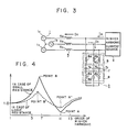
- Figs. 3 and 4 illustrate a conventional harmonic suppressor disclosed in Nisshin Denki Giho (technical report), issued by Nisshin Denki (electric appratus) Co., Ltd., Jan., l979.
- a distributing equipment comprises a three-phase AC power source l comprising AC power sources la, lb and lc, a higher harmonic current source 2 as a load such as, for example, a load cycloconverter, and, for example, a passive harmonic filtering device 3.
- An impedance 5 including inductive impedances 5a, 5b and 5c is produced in wires 4a, 4b and 4c forming a line 4 interconnecting the AC power sources, la, lb and lc and the higher harmonic current source 2.
- the harmonic filtering device 3 comprises a reactor 6, a capacitor 7 and a resistor 8.
- the reactor 6 includes reactors 6a, 6b and 6c respectively for the wires 4a, 4b and 4c
- the capacitor 7 includes capacitors 7a, 7b and 7c respectively for the wires 4a, 4b and 4c
- the resistor 8 includes resistances 8a, 8b and 8c respectively for the wires 4a, 4b and 4c.
- the higher harmonic current source 2 is, for example, a l2-phase cycloconverter
- the main components of the higher harmonic current I H produced by the cycloconverter are llth and l3th higher harmonics.
- the passive harmonic filtering device 3 is designed so as to be tuned at a frequency substantially corresponding to that of the llth harmonic. Since the impedance 5 of the line 4, in general, is an inductive impedance as mentioned above, a ratio I S /I H , where I H is a higher harmonic current produced in the circuit of Fig. 3 and I H is a higher harmonic current that flows into the power source l, has characteristics as shown in Fig. 4.
- the most part of the higher harmonic current I H is absorbed by the reactor 6 and capacitor 7 of the passive filter at a tuning point A near the llth higher harmonic, and hence curve representing the variation of the ratio I S /I H has a minimum at the point A as shown in Fig. 4.
- the curve of the ratio I S /I H has a maximum at a point B due to antiresonance between the harmonic filtering device 3 and the power source l, and the higher harmonic current increases.
- the degree of the increase of the higher harmonic current is dependent on the resistance of the resistor 8. When the resistance of the resistor 8 is small, the higher harmonic current is increased by a magnification in the range of ten to twenty, and thereby the extraordinarily large higher harmonic current I S flowing into the power source has injurious influences upon the power supply system.
- the conventional harmonic suppressor thus constituted inevitably has an antiresonance point, where the very large magnification of the higher harmonic current occurs. Accordingly, the passive filter of the harmonic suppressor is designed so that the antiresonance point thereof such as the point B shown in Fig. 4 will not coincide with the orders of higher harmonics to obviate the injurious influences of the magnified higher harmonic currents upon the power supply system.
- the higher harmonic current source 2 is a cycloconverter
- the order of a higher harmonic current necessarily coincides with the antiresonance point since the frequency of the generated higher harmonic current varies according to the output frequency of the cycloconverter as represented by Expression (3) shown hereinafter. Accordingly, it is impossible to obviate the occurrence of the very large magnification of the higher harmonic current.
- n is the order of a higher harmonic current
- f1 is the frequency of a fundamental wave
- f0 is the output frequency of the cycloconverter
- m and k are integral numbers.
- the frequency f5 of the fifth higher harmonic current varies in the range of 240 to 360Hz, namely, in the range of the fourth to sixth higher harmonic
- the frequency f7 of the seventh higher harmonic current varies in the range of 360 to 480Hz, namely, in the range of the sixth to the eighth higher harmonic
- the conventional passive filter is unable to avoid the magnification of higher harmonic currents at the antiresonance point when the frequency of the higher harmonic current is variable as the frequency of higher harmonic current produced by a cycloconverter, and hence such a conventional passive filter is unable to eliminate injurious influences on the associated system.
- the present invention provides a harmonic suppressing device having a high-order higher harmonic filtering unit, such as a passive filter, which absorbs higher harmonic currents of higher orders among the higher harmonic currents generated by a higher harmonic current source, and a low-order higher harmonic filtering unit, such as an active filter, which absorbs higher harmonic currents of lower orders among the higher harmonic currents generated by the higher harmonic current source.
- a possible low-order higher harmonic filtering units is a differentiating circuit which detects higher harmonic currents and processes the higher harmonic currents through phase-lead operation or a phase-lag network capable of first order lag operation.
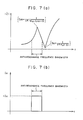
- FIG. 5 A first embodiment of the present invention will be described with reference to Figs. 5 to 7.
- parts denoted by reference numerals l to 7 are the same as or corresponds to those denoted by the same reference numerals in Fig. lA, and hence the description thereof will be omitted to avoid duplication.
- the harmonic suppressing device in a first embodiment comprises a passive filter 3 as a high-order higher harmonic filtering unit, an active filter l0 as a low-order higher harmonic filtering unit, and a higher harmonic current detector 9 which gives a detection signal upon the detection of an outflow higher harmonic current I S which flows into a power source l.
- the active filter l0 is a well-known device such as, for example, an inverter including a pulse width modulator (PWM), capable of generating an optional higher harmonic current I A of an optional frequency.
- PWM pulse width modulator
- the high-order higher harmonic filtering function of the harmonic suppressing device is substantially the same as that of the conventional passive filter previously described with reference to Figs. lA, lB and 2; the harmonic suppressing device absorbs higher harmonic currents from a higher harmonic current I H as shown in Fig. 7(a) by means of the reactor 6 and the capacitor 7.
- the higher harmonic current detector 9 detects an outflow higher harmonic current I S which flows into the power source l, and then gives a detection signal to the active filter l0.
- the harmonic suppressing device is able to suppress the outflow higher harmonic current I S to zero in the antiresonance frequency band by the output current I A of the active filter l0. Furthermore, since the passive filter 3 and the active filter l0 are employed in combination, the passive filter 3 is assigned to the resonance frequency band, while the active filter l0 is assigned to the antiresonance frequency band, the manufacturing cost of the harmonic suppressing device relating to the active filter is reduced, which is a characteristic effect of the first embodiment.
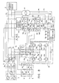
- a harmonic suppressing device in a second embodiment will be described hereinafter with reference to Figs. 8 to ll.
- Fig. 8 is a circuit diagram of a system, for example, a power distributing system, provided with a harmonic suppressing device in the second embodiment of the present invention.
- parts similar to or corresponding to those previously described with reference to Figs. lA, 3 and 5 are denoted by the same reference numerals.
- the second embodiment is substantially the same in constitution as the first embodiment.
- the first embodiment represents the general constitution of the present invention
- the second embodiment and a third embodiment which will be described hereinafter, represent the detailed constitution of the present invention.
- an active filter l0 employed as the low-order higher harmonic filtering unit of the harmonic suppressing device comprises a reactor ll, a transistor switch l2 comprising switching transistors l2a to l2f each provided with a rectifying diode, and a capacitor l3.
- a supply current transforming circuit 9 is provided in the line 4 interconnecting the power source l and the higher harmonic current source 2 to detect the supply current of the power source l.
- the supply current transforming circuit 9 has current transformers 9a, 9b and 9c provided in the wires 4a, 4b and 4c, respectively, of the line 4.
- the current transformers 9a, 9b and 9c are connected to a higher harmonic current detecting circuit l4.
- the active filter l0 includes a current transforming circuit l5 for detecting the current flowing through the active filter l0.
- the current transforming circuit has current transformers l5a, l5b and l5c.
- the output of the current transforming circuit l5 is connected to a subtracting circuit l7 having subtracters l7a, l7b and l7c.
- the higher harmonic current detecting circuit l4 is connected through a gain control circuit l6 to the subtracting circuit l7.
- the subtracters l7a, l7b and l7c of the subtracting circuit l7 are connected to the amplifiers l8a, l8b and l8c, respectively, of an amplifying circuit l8.
- the amplifiers l8a, l8b and l8c and a voltage transformer l9 for detecting the respective voltages of the wires 4a, 4b and 4c of the line 4 are connected to an adding circuit 20 having adders 20a, 20b and 20c.
- a PWM control circuit 2l which gives control signals to the switching transistors l2a to l2f of the transistor switch l2 is connected to the adding circuit 20.
- a passive filter 3 comprises a reactor 6, a capacitor 7 and a resistro 8.
- an active filter l0 is represented by a variable current source.
- An outflow current transformer 9 for detecting a current which flows into a power source l is connected through an amplifying circuit l4 having an amplification factor G to the active filter l0.
- a higher harmonic current I H generated by the higher harmonic current source 2 flows toward the AC power source l. Then, a current I S expressed by the following Expression (4) is generated by a resonance circuit including the impedance 5 of the system.
- L0 inductance among the impedance 5
- L1 is the inductance of the reactor 6 of the passive filter 3
- C is the capacitance of the capacitor 7 of the passive filter 3
- R is the resistance of the resistor 8 of the passive filter 3
- Z S and Z F are the impedance of the power source and the filter, respectively.
- Z F is the impedance of the filter side
- Z S is the impedance of the power source side
- Z M Z F /(Z F +Z S )
- Z S L0S
- Fig. 10 shows the variation of I S /I H with the order of higher harmonic current for various values of G obtained from Expression (7).
- the higher harmonic magnification (I S /I H ) at the antiresonance point decreases with the increase of the compensating gain G of the active filter l0.
- the gain G is in the range of 3 to 5
- the value of I S /I H near the 6th higher harmonic current is not greater than one, namely, the magnification of the higher harmonic current by resonance does not occur.
- Fig. ll is a graph showing the current that flows through the active filter l0 obtained from Fig. l0. It is known from Fig. ll that the output current of the active filter l0 for higher harmonic currents of an order below the series resonance point of the passive filter 3 corresponds substantially to the current I H , and the output current I C of the active filter l0 is far smaller than the current I H for higher harmonic currents of orders above the series resonance point of the passive filter 3.
- the characteristics shown in Fig. ll have the following advantages.
- the higher harmonic current source is, for example, a l2-phase cycloconverter
- the principal higher harmonic currents generated by the cycloconverter is of the llth and the l3th.
- the active filter l0 To absorb all the llth and l3th higher harmonic currents by the active filter l0, the active filter l0 needs to be of a large capacity, and hence the active filter l0 is an expensive one.
- the llth and l3th higher harmonic currents namely, higher harmonic currents of comparatively high orders are absorbed by the comparatively inexpensive passive filter 3
- the magnification of higher harmonic currents of lower orders attributable to the passive filter 3 is suppressed by the active filter l0, and comparatively small 5th and 7th higher harmonic currents are absorbed by the active filter l0, the capacity of the active filter l0 may be comparatively small, which is economically advantageous.
- the harmonic suppressing device shown in Fig. 8 is a concrete example of a harmonic suppressing device having the foregoing advantage.
- the current I S which flows into the power source side is detected by the current transformers 9a, 9b and 9c.
- the current I S includes a fundamental component and higher harmonic components.
- the fundamental component is filtered by the higher harmonic current detecting circuit l4 to detect only the higher harmonic components.
- the subtracting circuit l7 calculates the respective differences ⁇ I a , ⁇ I b and ⁇ I c between the output currents I A , I B and I C of the active filter l0 and the currents I Ga , I Gb and I Gc , and then applies the difference to the amplifiers l8a, l8b and l8c, respectively, of the amplifying circuit l8.
- the amplifying circuit l8 After amplifying the differences ⁇ I a , ⁇ I b and ⁇ I c by an amplification factor K, the amplifying circuit l8 gives the amplified differences to the adders 20a, 20b and 20c, respectively, of the adding circuit 20.
- the adders 20a, 20b and 20c adds the amplified differences to the supply voltages V a , V b and V c , respectively, and give output voltages V la , V lb and V lc to the PWM control circuit 2l.
- the PWM control circuit 2l modulates the voltages V la , V lb and V lc by, for example, a carrier signal of a triangular waveform, and then gives the modulated PWM signals to the switching transistors l2a, l2b and l2c, respectively, of the transistor switch l2.
- the transistor switch l2 operates for closing and opening in response to the PWM signals to provide inverter output voltages E Ia , E Ib and E Ic corresponding to the control signals V Ia , V Ib and V Ic , respectively.
- I Aa (V a - E Ia )/X L
- I Ab (V b - E Ib )/X L
- I Ac (V c - E Ic )/X L flow through the active filter l0.
- I Aa , I Ab and I Ac are currents which flow through the phases of the active filter l0, respectively, and X L is the reactance of the reactor ll.
- the currents I Aa , I Ab and I Ac become equal to the currents I Ha , I Hb and I Hc , respectively, so that the active filter l0 is able to make the necessary currents I Ha , I Hb and I Hc flow.
- the gain G is not necessarily constant; the gain G may be varied according to the range of output of the active filter.
- the output of the active filter for high-order higher harmonic currents can be limited by selectively determining the time constant T s and thereby further fine adjustment of the assignment of load to the active filter and the passive filter is possible to provide an active filter having an optimum capacity.
- the G(s) is not necessarily a function including a first order lag element, but may be a function including a second order lag element or a function including a higher order lag element or a lead-lag element for the same effect as that described hereinbefore.
- the second embodiment employs a voltage inverter as the active filter
- the voltage inverter may be substituted by a current inverter for the same effect.
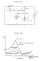
- a harmonic suppressing device in a third embodiment, according to the present invention will be described hereinafter with reference to Figs. 8, 9A, 9B, l2 and l3.
- the constitution of the circuit of the third embodiment is the same as that of the second embodiment shown in Fig. 8 and the single-phase equivalent circuits of the passive filter 3 serving as the high-order higher harmonic filtering unit and the active filter l0 serving as the low-order higher harmonic filtering unit of the third embodiment are substantially the same as those of the second embodiment.
- the PWM control circuit 2l employs the product of the higher harmonic components of the outflow current I S and the gain G obtained by the gain amplifier l6 as the transfer function.
- It is a particular feature of the third embodiment to employ a differentiation element for advancing the phase of the outflow higher harmonic current I S by 90° as a transfer function for the operating means of the active filter l0. Accordingly, the third embodiment will be described with reference to Fig. 8 regarding the gain circuit l6 of Fig. 8 as an operational circuit l6.
- the function of the active filter l0 is equivalent to a resistance 26 of an equivalent circuit of the harmonic suppressing device shown in Fig. l2.
- the equivalent circuit of Fig. l2 is used for calculating the distribution of higher harmonic currents.
- the outflow characteristics of the higher harmonic current in the circuit shown in Fig. l2 is determined in the following manner.
- the harmonic suppressing device thus constituted according to the present invention has the following advantages when applied to suppressing higher harmonic currents generated by, for example, l2-phase cycloconverter.
- the principal higher harmonic currents generated by the cycloconverter are llth, l3th, and 23rd, 25th higher harmonic currents.
- the active filter needs to have a very large capacity. Such an active filter is expensive.
- the llth and l3th higher harmonic currents and those of high orders above l3th are absorbed by a comparatively inexpensive passive filter, the magnification of low-order higher harmonic currents attributable to the passive filter is suppressed by an active filter, and comparatively small 5th and 7th higher harmonic currents due to unbalance between the six phases are absorbed by the active filter. Accordingly, the capacity of the active filter may be small, which is economically advantageous.
- the current transformers 9a, 9b and 9c detect the outflow current I S that flows into the power source side.
- the higher harmonic current detecting circuit l4 filters the fundamental component from the current I S to extract only the higher harmonic components.
- the higher harmonic components I Ha , I Hb and I Hc thus detected is applied to the operating circuits l6a, l6b and l6c, respectively, and are subjected to differential operation.
- the subtracters l7a, l7b and l7c calculate the difference between the currents I Ga m I Gb and I Gc , and the output currents I Aa , I Ab and I Ac of the active filter l0 detected by the transformers l5a, l5b and l5c, respectively, of the current transformer l5.
- the differences ⁇ I a , ⁇ I b and ⁇ I c are applied to the amplifiers l8a, l8b and l8c, respectively, of the amplifying circuit l8.
- the amplifying circuit l8 amplifies the differences ⁇ I a , ⁇ I b and ⁇ I c by an amplification factor K, and then gives the results of amplification to the adders 20a, 20b and 20c of the adding circuit 20.
- the adders 20a, 20b and 20c add the results of amplification and the corresponding supply voltages V Ia , V Ib and V Ic , respectively, and apply voltages V Ia , V Ib and V Ic to the PWM control circuit 2l.
- the PWM control circuit 2l modulates the input voltages V Ia , V Ib and V Ic , for example, by a triangular carrier signal, and then gives the modulated PWM signals to the switching transistors l2a to l2f.
- the switching transistors operate in response to the PWM signals to provide inverter output voltages E Ia , E Ib and E Ic respectively corresponding to the control signals V Ia , V Ib and V Ic .
- the transfer function G(s) is a differential characteristic T S
- the transfer function G(s) may be such as including first order differentiation element (l + T S ) or other differentiation element for the same effect as that of the third embodiment.
- first order differentiation element l + T S
- the output of the active filter for higher order higher harmonic currents can be limited by regulating the time constant T and thereby further fine adjustment of the assignment of load to the active filter and the passive filter is possible to provide an active filter having an optimum capacity.
- an active filter F is connected in parallel to a load L generating higher harmonics.
- a compensation current i H contained in a load current i L is operated to apply a compensation current i C to a set point.
- the active filter F functions as a higher harmonic current source and supplies, as a substitute for a power source P, a higher harmonic current required by the load L, and thereby the supply current contains only a fundamental wave current i B .
- a voltage type inverter employing a voltage source or a current type inverter employing a current source is an active filter which turns on and off a semiconductor switching device provided in the filter and which supplies the compensation current i C compensating the higher harmonic current i H .
- the active filter produces the compensation current i C as the compensation object from a DC voltage; the active filter operates at a response frequency exceeding the frequency of the compensation current i C ; therefore, the active filter needs to be capable of high-frequency switching operation of the semiconductor switching device.
- the switching frequency band in which the active filter is able to operate most effectively is low to middle frequency bands.
- FIG. l6 there are shown an AC power source l, a higher harmonic generating source 2 comprising a load such as a cycloconverter 30, a motor 3l controlled by the cycloconverter 30, a passive L-C filter 32 serving as a high-order higher harmonic filtering unit for compensating higher harmonics in a high-order frequency band.
- the passive L-C filter 32 is connected in parallel to the cycloconverter 30 to the same bus 40.
- a source current feedback type active filter l0 for compensating higher harmonics in low and middle frequency bands.
- the active filter l0 is capable of actively controlling the frequency of compensation higher harmonics.
- the source current feedback type active filter l0 comprises a voltage type inverter 34 and a current controller 35 for controlling the voltage type inverter 34.
- the source current feedback type active filter l0 detects the current of the power source by means of a current detector l5 and filters a fundamental wave current i B from the detected current to obtain a higher harmonic current i H to be compensated.
- the current controller 35 operates and amplifies the difference between the higher harmonic current i H and an output higher harmonic current component to provide a reference voltage. The reference voltage is applied after being subjected to PWM control to the voltage type inverter 34.
- the higher harmonic absorbing circuit has the passive L-C filter 32 which tunes with higher harmonics in a high frequency band, and the active filter l0 which effectively filters antiresonance which occurs in a low frequency band and higher harmonics in a middle frequency band.
- the harmonic suppressing device absorbs higher harmonics in a high frequency band by the passive L-C filter 32 and absorbs higher harmonics of the antiresonance and higher harmonics in a frequency band lower than the tuning frequency of the passive L-C filter 32 by the active filter l0 to eliminate the adverse influence of higher harmonics generated by the higher harmonic current generating source 2, namely, the load cycloconverter 30, on the component equipments of the power system.
- the cooperative function of the passive L-C filter 32 and the active filter l0 provides frequency characteristics eliminated of antiresonance.
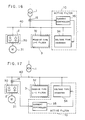
- a fifth embodiment of the present invention will be described with reference to Fig. l7.
- a current detector l5 for detecting a higher harmonic current i H generated by a load cycloconverter 30 is provided between the load cycloconverter 30 and a bus 40.
- the current detector l5 supplies the detected higher harmonic current i H to a current controller 35. Therefore, an active filter l0 employed in the fifth embodiment is a load current feedback active filter.
- the load current feedback active filter l0 comprises, as the basic components, a voltage type inverter 34 and the current controller 35 for controlling the current of the voltage type inverter 34.
- the load current feedback active filter l0 detects the difference between a command current and an actual current, then a hysteresis comparator discriminates the polarity of the difference and gives a signal corresponding to the polarity of the difference to a power semiconductor switching element to control the current.
- the sixth embodiment is substantially the same as the fourth embodiment in constitution, except that the source current feedback active filter l0 of the sixth embodiment comprises a current controller 35 and a current type inverter 44.
- the active filter l0 is of a source current feedback type
- a current detector l5 for detecting a higher harmonic current which flows into the AC power source l is provided near the AC power source l
- the inverter of the active filter l0 is the current type inverter 44.
- the current type inverter 44 is capable of directly controlling the output current of an objective cycloconverter control system.
- the current type inverter 44 controls the system current so that the frequency of the output current of the system is stabilized at a fixed frequency.
- An exemplary practical current type inverter is a series diode insertion type capacitance commutation inverter.
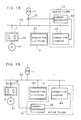
- FIG. l9 A seventh embodiment of the present invention will be described hereinafter.
- the seventh embodiment is the same as the fourth to sixth embodiments in the basic constitution.
- an AC power source l a cycloconverter 30, namely, a higher harmonic current generating source 2, and a high-order higher harmonic filtering unit 3 comprising a passive L-C filter 32.
- the seventh embodiment is characterized by the employment of a current type inverter 44 of a load current feedback system.
- a higher harmonic current generated by the cycloconverter 30, i.e., the load 2 is detected by a current detector l5 provided near the load 2.
- the difference between a command current and an actual current is detected on the basis of the current detected by the current detector l5 by a current controller 35 and the current type inverter 44, and then a hysteresis comparator discriminates the polarity of the difference, and then provides a signal corresponding to the polarity of the difference to control a power semiconductor switching element.
- the sixth and seventh embodiments have intrinsic excellent response characteristics in controlling the current of the power system owing to the employment of the current type inverter 44.
- the use of an active filter and a passive filter in combination enables the suppression of higher harmonic currents which flows into the power source circuit over the entire frequency band even if the frequencies of higher harmonic currents generated by the load are variable, and reduces the manufacturing cost of the harmonic suppressing device.
- the passive filter comprising a capacitor and a reactor
- the parallel resonance of the passive filter and the impedance of the power source circuit is suppressed and only the higher harmonic currents in a frequency band which cannot be absorbed by the passive filter is absorbed by the active filter connected in parallel to the passive filter
- the capacity of the active filter may be comparatively small, which reduces the manufacturing cost of the harmonic suppressing device capable of satisfactorily suppressing the magnification of higher harmonic currents.
- the harmonic suppressing device of the present invention is capable of suppressing the parallel resonance by advancing the phase of the higher harmonic currents that flows into the power source circuit by a fixed phase angle, higher harmonic currents are suppressed efficiently over a wide frequency band.
Abstract
Description
- The present invention relates to a harmonic suppressing device for suppressing higher harmonics generated by higher harmonic current sources provided in the power transmission system, power distributing system and/or power circuit of various industrial equipments and, more specifically, to a harmonic suppressing device for suppressing higher harmonics which are generated by a rectifier such as a thyristor, a nonlinear load equipment such as an arc furnace or the saturation of the core of a transformer, and cause various troubles such as noise generation, the overheat of the components of the equipments, television disturbance and faults in control systems.
- In recent years, higher harmonic troubles attributable particularly to semiconductor rectifiers employing thyristors or power converters comprising thyristors such as, for example, cycloconverters, occur frequently in power transmission systems and power distributing systems. Various measures have been taken with the progress of semiconductor techniques to eliminate such higher harmonic troubles.
- Figs. lA, lB and 2 are a circuit diagram, a circuit diagram of an equivalent circuit and a graph showing the characteristics of the equivalent circuit, respectively, of an exemplary conventional receiving and distributing equipment having the possibility of higher harmonic generation. Referring to Fig. lA, the receiving and distributing equipment comprises an AC power source l such as, for example, an AC generator, a higher harmonic
current source 2 which generates a higher harmonic current IH when driven by power supplied thereto from the AC power source l, namely, a load power converter such as, for example, a cycloconverter, and a passiveharmonic filtering device 3 for filtering higher harmonic currents generated by the higher harmoniccurrent source 2 such as, for example, a passive filter. The power source l and aline 4 produce a generator impedance and a line impedance, respectively. The sum of the generator impedance and the line impedance is indicated by an impedance (represented by a parameter "LPS")5. Theharmonic filtering device 3 such as, for example, a passive filter, is an LC tuning filter comprising, for example, an inductance 6 (represented by a parameter "Lf") and a capacitance 7 (represented by a parameter "Cf"). - The receiving and distributing equipment is represented by an equivalent circuit shown in Fig. lB. The impedance characteristics Z of LPS on the side of the load in Fig. lB, namely, the higher harmonic
current source 2, is shown in Fig. 2. - The operation of the receiving and distributing equipment thus constituted will be described hereinafter. Suppose that the frequency of a higher harmonic current IH produced by the higher harmonic
current source 2 is fR Higher harmonics attributable to the higher harmonic current IH are eliminated by theharmonic filtering device 3 by making the tuned frequency coincide with the frequency fR on the basis of the following Expression. - Tuned frequency = fR = l/2πLf·Cf ......(l)

where fR is the frequency of the higher harmonic current IH, Lf is the value of inductance of theinductance 6 of theharmonic filtering device 3, and Cf is the capacitance of thecapacitor 7 of theharmonic filtering device 3. Thus, the inductance Lf and the capacitance Cf are determined from Expression (l). - In Fig. lA, designated by IC and IS are a current that flows into the
harmonic filtering device 3 and a current that flows out from theharmonic filtering device 3 into the AC power source l, respectively. - In the
harmonic filtering device 3, since the tuned frequency is adjusted to fR to filter higher harmonic currents among the higher harmonic current IH, the current IS that flows into the AC power source l can be suppressed when the variation of the frequency fR of the higher harmonic current IH is moderate and is maintained substantially at a fixed level. However, when the frequency fR is variable, the higher harmonic current IS that flows into the AC power source l increases as the frequency fR approaches resonance frequency (antiresonance frequency) fAR between the impedance LPS and the passive filter, namely, theharmonic filtering device 3 in the foregoing equipment. Such a relation is expressed by
fAR = l/2π(Lf+LPS)·Cf ......(2)
Such a passive harmonic filtering device is unable to suppress higher harmonic currents effectively when the range of variation of the frequency fR including the antiresonance frequency fAR is wide. - Another exemplary harmonic suppressor connected to a three-phase AC power source among those which suppress higher harmonics on the above-mentioned principle of operation will be described hereinafter.
- Figs. 3 and 4 illustrate a conventional harmonic suppressor disclosed in Nisshin Denki Giho (technical report), issued by Nisshin Denki (electric appratus) Co., Ltd., Jan., l979. In Figs. 3 and 4, parts similar to or corresponding to those previously described with reference to Figs. lA and lB are denoted by the same reference characters. Referring to Fig. 3, a distributing equipment comprises a three-phase AC power source l comprising AC power sources la, lb and lc, a higher harmonic
current source 2 as a load such as, for example, a load cycloconverter, and, for example, a passiveharmonic filtering device 3. Animpedance 5 includinginductive impedances wires 4a, 4b and 4c forming aline 4 interconnecting the AC power sources, la, lb and lc and the higher harmoniccurrent source 2. Theharmonic filtering device 3 comprises areactor 6, acapacitor 7 and aresistor 8. Thereactor 6 includesreactors 6a, 6b and 6c respectively for thewires 4a, 4b and 4c, thecapacitor 7 includescapacitors wires 4a, 4b and 4c, while theresistor 8 includesresistances 8a, 8b and 8c respectively for thewires 4a, 4b and 4c. - The manner of operation of the
harmonic filtering device 3 will be described hereinafter. When the higher harmoniccurrent source 2 is, for example, a l2-phase cycloconverter, the main components of the higher harmonic current IH produced by the cycloconverter are llth and l3th higher harmonics. Accordingly, the passiveharmonic filtering device 3 is designed so as to be tuned at a frequency substantially corresponding to that of the llth harmonic. Since theimpedance 5 of theline 4, in general, is an inductive impedance as mentioned above, a ratio IS/IH, where IH is a higher harmonic current produced in the circuit of Fig. 3 and IH is a higher harmonic current that flows into the power source l, has characteristics as shown in Fig. 4. The most part of the higher harmonic current IH is absorbed by thereactor 6 andcapacitor 7 of the passive filter at a tuning point A near the llth higher harmonic, and hence curve representing the variation of the ratio IS/IH has a minimum at the point A as shown in Fig. 4. On the contrary, the curve of the ratio IS/IH has a maximum at a point B due to antiresonance between theharmonic filtering device 3 and the power source l, and the higher harmonic current increases. The degree of the increase of the higher harmonic current is dependent on the resistance of theresistor 8. When the resistance of theresistor 8 is small, the higher harmonic current is increased by a magnification in the range of ten to twenty, and thereby the extraordinarily large higher harmonic current IS flowing into the power source has injurious influences upon the power supply system. - The conventional harmonic suppressor thus constituted inevitably has an antiresonance point, where the very large magnification of the higher harmonic current occurs. Accordingly, the passive filter of the harmonic suppressor is designed so that the antiresonance point thereof such as the point B shown in Fig. 4 will not coincide with the orders of higher harmonics to obviate the injurious influences of the magnified higher harmonic currents upon the power supply system.
- However, when the higher harmonic
current source 2 is a cycloconverter, the order of a higher harmonic current necessarily coincides with the antiresonance point since the frequency of the generated higher harmonic current varies according to the output frequency of the cycloconverter as represented by Expression (3) shown hereinafter. Accordingly, it is impossible to obviate the occurrence of the very large magnification of the higher harmonic current. - The frequency fn of an nth higher harmonic current is expressed by
fn = (6m±l)f₁ ± 6k·f₀ ......(3)
where n is the order of a higher harmonic current, f₁ is the frequency of a fundamental wave, f₀ is the output frequency of the cycloconverter, and m and k are integral numbers. - For example, when m = l, f₁ = 60Hz, f₀ = 0 to l0Hz, and k = l, the frequency f₅ of the fifth higher harmonic current varies in the range of 240 to 360Hz, namely, in the range of the fourth to sixth higher harmonic, while the frequency f₇ of the seventh higher harmonic current varies in the range of 360 to 480Hz, namely, in the range of the sixth to the eighth higher harmonic, so that the frequency varies continuously in the range of the fourth to the eighth higher harmonic when both the fifth and seventh higher harmonic currents are taken into consideration. Therefore, a higher harmonic current of an order which coincides with the antiresonance point B (Fig. 4) is produced inevitably.
- In the l2-phase cycloconverter, higher harmonic currents of orders above the fifth are produced and, theoretically, the fifth higher harmonic current or the seventh higher harmonic current cannot be produced. However, in practice, the fifth and seventh higher harmonic currents are produced due to unbalance between the six phases, and the fifth and seventh higher harmonic currents are magnified by resonance.
- Thus, the conventional passive filter is unable to avoid the magnification of higher harmonic currents at the antiresonance point when the frequency of the higher harmonic current is variable as the frequency of higher harmonic current produced by a cycloconverter, and hence such a conventional passive filter is unable to eliminate injurious influences on the associated system.
- Furthermore, in the conventional passive filter, it is necessary to increase the resistance of the
reactor 8 to reduce the ratio of higher harmonic magnification. However, although the ratio of higher harmonic magnification at the antiresonance point Bʹ is reduced when the resistance of thereactor 8 is increased, the higher harmonic absorption ratio near the resonance point Aʹ is reduced and electrical loss across theresistor 8 increases. - Accordingly, it is an object of the present invention to provide a harmonic suppressing device capable of suppressing antiresonance and absorbing higher harmonic current even if the frequency of the higher harmonic current generated by a higher harmonic current source varies over a wide range including the antiresonance point and the resonance point.
- It is a further object of the present invention to provide a harmonic suppressing device capable of preventing the magnification of higher harmonic currents at the antiresonance point even when the higher harmonic current source is a cycloconverter, and capable of preventing injurious influences of higher harmonic currents on the associated system such as, for example, a power generating system, a power transmission system or a power distributing system.
- It is still a further object of the present invention to provide a harmonic suppressing device employing a resistor having an ordinary resistance for reducing the ratio of magnification of higher harmonic currents and hence capable of preventing the reduction of higher harmonic absorption ratio at the resonance point (point Aʹ) and suppressing the increase of electrical loss attributable to the increase of the resistance of the resistor.
- To achieve the foregoing objects of the invention, the present invention provides a harmonic suppressing device having a high-order higher harmonic filtering unit, such as a passive filter, which absorbs higher harmonic currents of higher orders among the higher harmonic currents generated by a higher harmonic current source, and a low-order higher harmonic filtering unit, such as an active filter, which absorbs higher harmonic currents of lower orders among the higher harmonic currents generated by the higher harmonic current source. A possible low-order higher harmonic filtering units is a differentiating circuit which detects higher harmonic currents and processes the higher harmonic currents through phase-lead operation or a phase-lag network capable of first order lag operation.
-
- Figures lA and lB are a circuit diagram and an equivalent circuit diagram, respectively, of an exemplary conventional passive filter;
- Figure 2 is a graph showing the characteristics of higher harmonic currents in the circuit shown in Figs. lA and lB;
- Figure 3 is a circuit diagram of another exemplary conventional three-phase AC harmonic suppressing device;
- Figure 4 is a graph showing the characteristics of higher harmonic currents in a system associated with the harmonic suppressing device of Fig. 3;
- Figure 5 is a circuit diagram of a harmonic suppressing device, in a first embodiment, according to the present invention;
- Figure 6 is an equivalent circuit of the harmonic suppressing device of Fig. 5;
- Figures 7(a) and 7(b) are a graph showing the impedance characteristics of the equivalent circuit of Fig. 6 and a graph showing a waveform indicating the operating range of the harmonic suppressing device of Fig. 5, respectively;
- Figure 8 is a circuit diagram of a harmonic suppressing device, in a second embodiment, according to the present invention;
- Figures 9A and 9B are a circuit diagram of a passive filter employed as the high-order higher harmonic filtering unit of the second embodiment, and an active filter employed as the low-order higher harmonic filtering unit of the second embodiment, respectively;
- Figure l0 is a graph showing the variation of higher harmonic current magnification ratio (IS/IH) with the order of higher harmonic currents for gain G;
- Figure ll is a graph showing a mode of variation of current (IA/IH) which flows into the active filter when gain G = 5;
- Figure l2 is a circuit diagram of an equivalent circuit of a harmonic suppressing device, in a third embodiment, according to the present invention;
- Figure l3 is a graph showing the antiresonance damping effect of an active filter employed as the low-order higher harmonic filtering unit of the third embodiment;
- Figure l4 is a block diagram of assistance in explaining the principle of a harmonic suppressing device according to the present invention, showing the disposition of an active filter in an associated circuit;
- Figures l5(a), l5(b) and l5(c) are current waveform charts of assistance in explaining the principle of compensation function of the active filter of Fig. l4;
- Figure l6 is a block diagram of a harmonic suppressing device, in a fourth embodiment, according to the present invention;
- Figure l7 is a block diagram of a harmonic suppressing device, in a fifth embodiment, according to the present invention;
- Figure l8 is a block diagram of a harmonic suppressing device, in a sixth embodiment, according to the present invention; and
- Figure l9 is a block diagram of a harmonic suppressing device, in a seventh embodiment according to the present invention.
- Harmonic suppressing devices, in preferred embodiments, according to the present invention will be described hereinafter with reference to the accompanying drawings.
- A first embodiment of the present invention will be described with reference to Figs. 5 to 7. In Fig. 5, parts denoted by reference numerals l to 7 are the same as or corresponds to those denoted by the same reference numerals in Fig. lA, and hence the description thereof will be omitted to avoid duplication.
- The harmonic suppressing device in a first embodiment comprises a
passive filter 3 as a high-order higher harmonic filtering unit, an active filter l0 as a low-order higher harmonic filtering unit, and a higher harmoniccurrent detector 9 which gives a detection signal upon the detection of an outflow higher harmonic current IS which flows into a power source l. The active filter l0 is a well-known device such as, for example, an inverter including a pulse width modulator (PWM), capable of generating an optional higher harmonic current IA of an optional frequency. - The manner of operation of the harmonic suppressing device will be described hereinafter. The high-order higher harmonic filtering function of the harmonic suppressing device is substantially the same as that of the conventional passive filter previously described with reference to Figs. lA, lB and 2; the harmonic suppressing device absorbs higher harmonic currents from a higher harmonic current IH as shown in Fig. 7(a) by means of the
reactor 6 and thecapacitor 7. The higher harmoniccurrent detector 9 detects an outflow higher harmonic current IS which flows into the power source l, and then gives a detection signal to the active filter l0. Upon the reception of the detection signal from the higher harmoniccurrent detector 9, the output level and output frequency of the active filter l0 are controlled so as to generate a higher harmonic current IA = -IH as shown in Fig. 7(b) in an antiresonance frequency band in which the outflow higher harmonic current IS increases to cancel the higher harmonic currents in the neighborhood of the antiresonance point. - Thus, the harmonic suppressing device is able to suppress the outflow higher harmonic current IS to zero in the antiresonance frequency band by the output current IA of the active filter l0. Furthermore, since the
passive filter 3 and the active filter l0 are employed in combination, thepassive filter 3 is assigned to the resonance frequency band, while the active filter l0 is assigned to the antiresonance frequency band, the manufacturing cost of the harmonic suppressing device relating to the active filter is reduced, which is a characteristic effect of the first embodiment. - A harmonic suppressing device in a second embodiment will be described hereinafter with reference to Figs. 8 to ll.
- Fig. 8 is a circuit diagram of a system, for example, a power distributing system, provided with a harmonic suppressing device in the second embodiment of the present invention. In Fig. 8, parts similar to or corresponding to those previously described with reference to Figs. lA, 3 and 5 are denoted by the same reference numerals. Fundamentally, the second embodiment is substantially the same in constitution as the first embodiment. Whereas the first embodiment represents the general constitution of the present invention, the second embodiment and a third embodiment, which will be described hereinafter, represent the detailed constitution of the present invention.
- Referring to Fig. 8, an active filter l0 employed as the low-order higher harmonic filtering unit of the harmonic suppressing device comprises a reactor ll, a transistor switch l2 comprising switching transistors l2a to l2f each provided with a rectifying diode, and a capacitor l3. A supply
current transforming circuit 9 is provided in theline 4 interconnecting the power source l and the higher harmoniccurrent source 2 to detect the supply current of the power source l. The supplycurrent transforming circuit 9 has current transformers 9a, 9b and 9c provided in thewires 4a, 4b and 4c, respectively, of theline 4. The current transformers 9a, 9b and 9c are connected to a higher harmonic current detecting circuit l4. The active filter l0 includes a current transforming circuit l5 for detecting the current flowing through the active filter l0. The current transforming circuit has current transformers l5a, l5b and l5c. The output of the current transforming circuit l5 is connected to a subtracting circuit l7 having subtracters l7a, l7b and l7c. The higher harmonic current detecting circuit l4 is connected through a gain control circuit l6 to the subtracting circuit l7. The subtracters l7a, l7b and l7c of the subtracting circuit l7 are connected to the amplifiers l8a, l8b and l8c, respectively, of an amplifying circuit l8. The amplifiers l8a, l8b and l8c and a voltage transformer l9 for detecting the respective voltages of thewires 4a, 4b and 4c of theline 4 are connected to an addingcircuit 20 havingadders circuit 20. - The manner of operation of the harmonic suppressing device in the second embodiment will be described hereinafter. First, the principle of operation based on the fundamental constitution shown in Fig. 8 will be described with reference to simplified circuits shown in Figs. 9A and 9B showing a single-phase equivalent circuit of the passive filter serving as a high-order higher harmonic filtering unit, and a single-phase equivalent circuit of the harmonic suppressing device including the active filter serving as a low-order higher harmonic filtering unit, respectively.
- Referring to Fig. 9A, a
passive filter 3 comprises areactor 6, acapacitor 7 and aresistro 8. In Fig. 9B, an active filter l0 is represented by a variable current source. An outflowcurrent transformer 9 for detecting a current which flows into a power source l is connected through an amplifying circuit l4 having an amplification factor G to the active filter l0. - Referring to Figs. 9A and 9B, a higher harmonic current IH generated by the higher harmonic
current source 2 flows toward the AC power source l. Then, a current IS expressed by the following Expression (4) is generated by a resonance circuit including theimpedance 5 of the system. - IS = IH·ZF/(ZF+ZS) ......(4)
ZS = L₀·S
ZF = Ll·S+1/C·S where L₀ is inductance among theimpedance 5, L₁ is the inductance of thereactor 6 of thepassive filter 3, C is the capacitance of thecapacitor 7 of thepassive filter 3, R is the resistance of theresistor 8 of thepassive filter 3, and ZS and ZF are the impedance of the power source and the filter, respectively. - From Expression (4), it is known that the higher harmonic current is magnified in a range where |ZF+ZS| < |ZF|. Such a higher harmonic current of a comparatively low-order is filtered by the active filter l0 shown in Fig. 9B.
- The current transformer 9 (Fig. 9B) detects the outflow current IS, and then the amplifying circuit l4 amplifies the outflow current IS by the amplification factor G to supply a current G·IS to the active filter l0. Consequently, the higher harmonic current IS which flows through the power source l is
IS = (IH-G·IS) - IC ......(5) - On the other hand, the higher harmonic current IS is expressed by
IS = ZF(IH-G·IS)/(ZF+ZS) = ZM(IH-G·IS) ......(6)
where ZF is the impedance of the filter side, ZS is the impedance of the power source side, ZM = ZF/(ZF+ZS), ZS = L₀S and ZF = L₁S + 1/CS + R. Therefore,
IS/IH = ZM/(1+G·ZM) ......(7) - Fig. 10 shows the variation of IS/IH with the order of higher harmonic current for various values of G obtained from Expression (7).
- Referring to Fig. l0, a condition G = 0 corresponds to the omission of the active filter l0, and the
passive filter 3 has a series resonance point for the llth higher harmonic current and an antiresonance point for the 6th higher harmonic current. When G = 0, the higher harmonic current is magnified by approximately twenty times near the antiresonance point. - The higher harmonic magnification (IS/IH) at the antiresonance point decreases with the increase of the compensating gain G of the active filter l0. When the gain G is in the range of 3 to 5, the value of IS/IH near the 6th higher harmonic current is not greater than one, namely, the magnification of the higher harmonic current by resonance does not occur.
- Fig. ll is a graph showing the current that flows through the active filter l0 obtained from Fig. l0. It is known from Fig. ll that the output current of the active filter l0 for higher harmonic currents of an order below the series resonance point of the
passive filter 3 corresponds substantially to the current IH, and the output current IC of the active filter l0 is far smaller than the current IH for higher harmonic currents of orders above the series resonance point of thepassive filter 3. The characteristics shown in Fig. ll have the following advantages. When the higher harmonic current source is, for example, a l2-phase cycloconverter, the principal higher harmonic currents generated by the cycloconverter is of the llth and the l3th. To absorb all the llth and l3th higher harmonic currents by the active filter l0, the active filter l0 needs to be of a large capacity, and hence the active filter l0 is an expensive one. When the llth and l3th higher harmonic currents, namely, higher harmonic currents of comparatively high orders are absorbed by the comparatively inexpensivepassive filter 3, the magnification of higher harmonic currents of lower orders attributable to thepassive filter 3 is suppressed by the active filter l0, and comparatively small 5th and 7th higher harmonic currents are absorbed by the active filter l0, the capacity of the active filter l0 may be comparatively small, which is economically advantageous. - The harmonic suppressing device shown in Fig. 8 is a concrete example of a harmonic suppressing device having the foregoing advantage.
- Referring to Fig. 8, the current IS which flows into the power source side is detected by the current transformers 9a, 9b and 9c. The current IS includes a fundamental component and higher harmonic components. The fundamental component is filtered by the higher harmonic current detecting circuit l4 to detect only the higher harmonic components. The higher harmonic components IHa, IHb and IHc are applied to the gain amplifier l6a, l6b and l6c of the gain circuit l6, respectively, where the higher harmonic components are multiplied by the gain G to provide
IGa = G·IHa
IGb = G·IHb
IGc = G·IHc The currents IGa, IGb and IGc are applied to the subtracters l7a, l7b and l7c, respectively, of the subtracting circuit l7. The subtracting circuit l7 calculates the respective differences ΔIa, ΔIb and ΔIc between the output currents IA, IB and IC of the active filter l0 and the currents IGa, IGb and IGc, and then applies the difference to the amplifiers l8a, l8b and l8c, respectively, of the amplifying circuit l8. - After amplifying the differences ΔIa, ΔIb and ΔIc by an amplification factor K, the amplifying circuit l8 gives the amplified differences to the
adders circuit 20. Theadders - The transistor switch l2 operates for closing and opening in response to the PWM signals to provide inverter output voltages EIa, EIb and EIc corresponding to the control signals VIa, VIb and VIc, respectively.
- Consequently, currents
IAa = (Va - EIa)/XL
IAb = (Vb - EIb)/XL
IAc = (Vc - EIc)/XL flow through the active filter l0. IAa, IAb and IAc are currents which flow through the phases of the active filter l0, respectively, and XL is the reactance of the reactor ll. - When the gain K is sufficiently large, the currents IAa, IAb and IAc become equal to the currents IHa, IHb and IHc, respectively, so that the active filter l0 is able to make the necessary currents IHa, IHb and IHc flow. The output current IA of the active filter l0 thus controlled is G times the higher harmonic component of the outflow current IS, and hence
IA = G·IH
Therefore, the characteristic curves as shown in Figs. l0 and ll are obtained. - The gain G is not necessarily constant; the gain G may be varied according to the range of output of the active filter. For example, the gain G may be a variable defined by
G = G₀/(l + Ts)
where G₀ is a constant and Ts is a time constant. The output of the active filter for high-order higher harmonic currents can be limited by selectively determining the time constant Ts and thereby further fine adjustment of the assignment of load to the active filter and the passive filter is possible to provide an active filter having an optimum capacity. - The G(s) is not necessarily a function including a first order lag element, but may be a function including a second order lag element or a function including a higher order lag element or a lead-lag element for the same effect as that described hereinbefore.
- Although the second embodiment employs a voltage inverter as the active filter, the voltage inverter may be substituted by a current inverter for the same effect.
- A harmonic suppressing device, in a third embodiment, according to the present invention will be described hereinafter with reference to Figs. 8, 9A, 9B, l2 and l3.
- Basically, the constitution of the circuit of the third embodiment is the same as that of the second embodiment shown in Fig. 8 and the single-phase equivalent circuits of the
passive filter 3 serving as the high-order higher harmonic filtering unit and the active filter l0 serving as the low-order higher harmonic filtering unit of the third embodiment are substantially the same as those of the second embodiment. In the second embodiment, the PWM control circuit 2l employs the product of the higher harmonic components of the outflow current IS and the gain G obtained by the gain amplifier l6 as the transfer function. It is a particular feature of the third embodiment to employ a differentiation element for advancing the phase of the outflow higher harmonic current IS by 90° as a transfer function for the operating means of the active filter l0. Accordingly, the third embodiment will be described with reference to Fig. 8 regarding the gain circuit l6 of Fig. 8 as an operational circuit l6. - A transfer function for the operational circuit l6 includes a differentiation element for advancing the phase of the outflow higher harmonic current IS by 90° and is expressed by
G(s) = Ts ......(8)
where Ts is a time constant for differential operation. - When the active filter l0 is thus controlled, the function of the active filter l0 is equivalent to a
resistance 26 of an equivalent circuit of the harmonic suppressing device shown in Fig. l2. Acurrent source 27 of the equivalent circuit of Fig. l2 corresponding to the higher harmoniccurrent source 2. The equivalent circuit of Fig. l2 is used for calculating the distribution of higher harmonic currents. When a higher harmonic current IS flows through the power source side, a voltage VL across the impedance L₀ of the system is expressed by
VL = L₀S·I₀ ......(9) therefore, a current IR that flows through theresistance 26 is
IR = VL/R₀ = (L₀S/R₀)·IS ......(l0) - On the other hand, according to the control system of the present invention, the current IA that flows through the active filter l0 of Fig. 9B is expressed by IA = G(s)·IS = TS·IS ......(ll) when T = L₀/R₀, Expressions (l0) and (ll) coincide with each other, and hence the circuits shown in Figs. 9B and l2 are entirely equivalent to each other.
- Accordingly, the outflow characteristics of the higher harmonic current in the circuit shown in Fig. l2 is determined in the following manner.
- The impedance ZFl of the
passive filter 3 is
ZFl = Lls + l/cs ......(l2)
Therefore, the total impedance ZF of the higher harmonic filter side including the dampingresistance 26 is
ZF = R₀·ZFl/(R₀ + ZFl) ......(l3) and the higher harmonic current IS that flows into the power source side is
IS = IH·ZF/(ZS + ZF) ......(l4)
provided that ZS = L₀·s. - From Expression (l4) frequency characteristics curves shown in Fig. l3 is obtained. As is obvious from Fig. l3, the higher harmonic magnification (IS/IH) at the antiresonance point B decreases with the decrease of R₀, and IS/IH < l over the entire range of higher harmonic currents as indicated by a curve (c) in Fig. l3 when the resistance R₀ of the damping
resistance 26 is selected properly. Thus, the harmonic suppressing device is capable of absorbing higher harmonic currents in a wide frequency band without magnifying higher harmonic currents. - Since the characteristics of the damping
resistor 26 shown in Fig. l2 can be realized by the control characteristics of the active filter l0, there is no practical loss attributable to the resistance R₀ of theresistor 26 and hence the harmonic suppressing device is able to operate at a high efficiency. - Furthermore, since most of the higher harmonic currents in a high-order higher harmonic frequency band above the llth higher harmonic current is filtered by the
passive filter 3 and hence the active filter l0 need not have a capacity to filter such higher harmonic currents, which is economically advantageous. - The harmonic suppressing device thus constituted according to the present invention has the following advantages when applied to suppressing higher harmonic currents generated by, for example, l2-phase cycloconverter. The principal higher harmonic currents generated by the cycloconverter are llth, l3th, and 23rd, 25th higher harmonic currents. To absorb all those principal higher harmonic currents by an active filter, the active filter needs to have a very large capacity. Such an active filter is expensive. According to the present invention, the llth and l3th higher harmonic currents and those of high orders above l3th are absorbed by a comparatively inexpensive passive filter, the magnification of low-order higher harmonic currents attributable to the passive filter is suppressed by an active filter, and comparatively small 5th and 7th higher harmonic currents due to unbalance between the six phases are absorbed by the active filter. Accordingly, the capacity of the active filter may be small, which is economically advantageous.
- The third embodiment using a differential function will be described more concretely hereinafter with reference to Fig. 8.
- The current transformers 9a, 9b and 9c detect the outflow current IS that flows into the power source side. The higher harmonic current detecting circuit l4 filters the fundamental component from the current IS to extract only the higher harmonic components. The higher harmonic components IHa, IHb and IHc thus detected is applied to the operating circuits l6a, l6b and l6c, respectively, and are subjected to differential operation.
IGa = G(s)·IHa = TS·IHa
IGb = G·IHb = TS·IHb
IGc = G·IHc = TS·IHc and then the results of the differential operation is applied to the subtracting circuit l7. - Then, the subtracters l7a, l7b and l7c calculate the difference between the currents IGam IGb and IGc, and the output currents IAa, IAb and IAc of the active filter l0 detected by the transformers l5a, l5b and l5c, respectively, of the current transformer l5. Then, the differences ΔIa, ΔIb and ΔIc are applied to the amplifiers l8a, l8b and l8c, respectively, of the amplifying circuit l8.
- The amplifying circuit l8 amplifies the differences ΔIa, ΔIb and ΔIc by an amplification factor K, and then gives the results of amplification to the
adders circuit 20. Theadders - The switching transistors operate in response to the PWM signals to provide inverter output voltages EIa, EIb and EIc respectively corresponding to the control signals VIa, VIb and VIc.
- Consequently, the currents IAa, IAb and IAc that flow through the phases, respectively, of the active filter l0 are
IAa = (Va - EIa)/XL
IAb = (Vb - EIb)/XL
IAc = (Vc - EIc)/XL where XL is the reactance of the reactor ll. - When the gain K is sufficiently large, the currents IHa, IHb and IHc and the corresponding currents IAa, IAb and IAc coincide with each other, and thereby the active filter l0 is able to make the necessary currents IHa, IHb and IHc. The output current IA of the active filter l0 thus controlled is G(s) times the higher harmonic component of the outflow current IS that flows into the power source side. Therefore,
IA = G(s)·IH = TS·IH
Thus, the characteristics shown in Figs. l2 and l3 are obtained. - In the foregoing description, the transfer function G(s) is a differential characteristic TS, however, the transfer function G(s) may be such as including first order differentiation element (l + TS) or other differentiation element for the same effect as that of the third embodiment. For example, when G(s) = l + TS, the output of the active filter for higher order higher harmonic currents can be limited by regulating the time constant T and thereby further fine adjustment of the assignment of load to the active filter and the passive filter is possible to provide an active filter having an optimum capacity.
- Prior to the description of fourth to seventh embodiments of the present invention, the principle of compensation function of an active filter will be described with reference to Figs. l4 and l5.
- As shown in Fig. l4, an active filter F is connected in parallel to a load L generating higher harmonics. Referring to Figs. l5(a), l5(b) and l5(c) showing the principle of compensation of higher harmonics generated by a six-pulse rectifier included, by way of example, as a load in a system, a compensation current iH contained in a load current iL is operated to apply a compensation current iC to a set point. Thus, the active filter F functions as a higher harmonic current source and supplies, as a substitute for a power source P, a higher harmonic current required by the load L, and thereby the supply current contains only a fundamental wave current iB.
- A voltage type inverter employing a voltage source or a current type inverter employing a current source is an active filter which turns on and off a semiconductor switching device provided in the filter and which supplies the compensation current iC compensating the higher harmonic current iH. The active filter produces the compensation current iC as the compensation object from a DC voltage; the active filter operates at a response frequency exceeding the frequency of the compensation current iC; therefore, the active filter needs to be capable of high-frequency switching operation of the semiconductor switching device. However, since the operation speed of the semiconductor switching device is limited, the switching frequency band in which the active filter is able to operate most effectively is low to middle frequency bands.
- A fourth embodiment of the present invention will be described hereinafter. Referring to Fig. l6, there are shown an AC power source l, a higher
harmonic generating source 2 comprising a load such as acycloconverter 30, a motor 3l controlled by thecycloconverter 30, a passiveL-C filter 32 serving as a high-order higher harmonic filtering unit for compensating higher harmonics in a high-order frequency band. The passiveL-C filter 32 is connected in parallel to thecycloconverter 30 to thesame bus 40. Also shown in Fig. l6 is a source current feedback type active filter l0 for compensating higher harmonics in low and middle frequency bands. The active filter l0 is capable of actively controlling the frequency of compensation higher harmonics. The source current feedback type active filter l0 comprises avoltage type inverter 34 and acurrent controller 35 for controlling thevoltage type inverter 34. The source current feedback type active filter l0 detects the current of the power source by means of a current detector l5 and filters a fundamental wave current iB from the detected current to obtain a higher harmonic current iH to be compensated. Thecurrent controller 35 operates and amplifies the difference between the higher harmonic current iH and an output higher harmonic current component to provide a reference voltage. The reference voltage is applied after being subjected to PWM control to thevoltage type inverter 34. - Thus, the higher harmonic absorbing circuit has the passive
L-C filter 32 which tunes with higher harmonics in a high frequency band, and the active filter l0 which effectively filters antiresonance which occurs in a low frequency band and higher harmonics in a middle frequency band. - In operation, the harmonic suppressing device absorbs higher harmonics in a high frequency band by the passive
L-C filter 32 and absorbs higher harmonics of the antiresonance and higher harmonics in a frequency band lower than the tuning frequency of the passiveL-C filter 32 by the active filter l0 to eliminate the adverse influence of higher harmonics generated by the higher harmoniccurrent generating source 2, namely, theload cycloconverter 30, on the component equipments of the power system. Thus, the cooperative function of the passiveL-C filter 32 and the active filter l0 provides frequency characteristics eliminated of antiresonance. - A fifth embodiment of the present invention will be described with reference to Fig. l7. In the fifth embodiment, a current detector l5 for detecting a higher harmonic current iH generated by a
load cycloconverter 30 is provided between theload cycloconverter 30 and abus 40. The current detector l5 supplies the detected higher harmonic current iH to acurrent controller 35. Therefore, an active filter l0 employed in the fifth embodiment is a load current feedback active filter. - The load current feedback active filter l0 comprises, as the basic components, a
voltage type inverter 34 and thecurrent controller 35 for controlling the current of thevoltage type inverter 34. The load current feedback active filter l0 detects the difference between a command current and an actual current, then a hysteresis comparator discriminates the polarity of the difference and gives a signal corresponding to the polarity of the difference to a power semiconductor switching element to control the current. - A sixth embodiment of the present invention will be described hereinafter. Referring to Fig. l8, the sixth embodiment is substantially the same as the fourth embodiment in constitution, except that the source current feedback active filter l0 of the sixth embodiment comprises a
current controller 35 and acurrent type inverter 44. Since the active filter l0 is of a source current feedback type, a current detector l5 for detecting a higher harmonic current which flows into the AC power source l is provided near the AC power source l, and the inverter of the active filter l0 is thecurrent type inverter 44. Thecurrent type inverter 44 is capable of directly controlling the output current of an objective cycloconverter control system. Thecurrent type inverter 44 controls the system current so that the frequency of the output current of the system is stabilized at a fixed frequency. An exemplary practical current type inverter is a series diode insertion type capacitance commutation inverter. - A seventh embodiment of the present invention will be described hereinafter. Referring to Fig. l9, the seventh embodiment is the same as the fourth to sixth embodiments in the basic constitution. In Fig. l9, there are shown an AC power source l, a
cycloconverter 30, namely, a higher harmoniccurrent generating source 2, and a high-order higherharmonic filtering unit 3 comprising a passiveL-C filter 32. The seventh embodiment is characterized by the employment of acurrent type inverter 44 of a load current feedback system. A higher harmonic current generated by thecycloconverter 30, i.e., theload 2, is detected by a current detector l5 provided near theload 2. Then, the difference between a command current and an actual current is detected on the basis of the current detected by the current detector l5 by acurrent controller 35 and thecurrent type inverter 44, and then a hysteresis comparator discriminates the polarity of the difference, and then provides a signal corresponding to the polarity of the difference to control a power semiconductor switching element. - The sixth and seventh embodiments have intrinsic excellent response characteristics in controlling the current of the power system owing to the employment of the
current type inverter 44. - As apparent from the foregoing description of the preferred embodiments of the present invention, the use of an active filter and a passive filter in combination enables the suppression of higher harmonic currents which flows into the power source circuit over the entire frequency band even if the frequencies of higher harmonic currents generated by the load are variable, and reduces the manufacturing cost of the harmonic suppressing device.
- Furthermore, since the principal higher harmonic currents among the higher harmonic currents generated by the load is absorbed by the passive filter comprising a capacitor and a reactor, and the parallel resonance of the passive filter and the impedance of the power source circuit is suppressed and only the higher harmonic currents in a frequency band which cannot be absorbed by the passive filter is absorbed by the active filter connected in parallel to the passive filter, the capacity of the active filter may be comparatively small, which reduces the manufacturing cost of the harmonic suppressing device capable of satisfactorily suppressing the magnification of higher harmonic currents.
- Still further, since the harmonic suppressing device of the present invention is capable of suppressing the parallel resonance by advancing the phase of the higher harmonic currents that flows into the power source circuit by a fixed phase angle, higher harmonic currents are suppressed efficiently over a wide frequency band.
Claims (19)
a high-order higher harmonic filtering unit for filtering high-order higher harmonic currents in a predetermined frequency band including a tuned frequency band; and
a low-order higher harmonic filtering unit for filtering low-order higher harmonic currents in a fixed frequency band other than the tuned frequency band.
a passive filter comprising a series connection of a capacitor and a reactor, and serving as a high-order higher harmonic filtering unit for filtering higher harmonic currents of comparatively high orders in a frequency band around a tuned point among higher harmonic currents generated by the higher harmonic current source of a power system; and
an active filter serving as a low-order higher harmonic filtering unit for filtering higher harmonic currents of comparatively low orders in a frequency band around an antiresonance point among those generated by said higher harmonic current source, connected in parallel to said passive filter and adapted so as to be controlled on the basis of a value obtained by multiplying the detected value of a higher harmonic current that flows into the power source side beyond the connecting point of said passive filter and a power source by a fixed gain.
a passive filter serving as a high-order higher harmonic filtering unit comprising a series connection of a capacitor and a reactor, and capable of filtering higher harmonic currents of comparatively high orders in a frequency band around a tuned point among those generated by a higher harmonic current source; and
an active filter serving as a low-order higher harmonic filtering unit for filtering higher harmonic currents of comparatively low orders in a frequency band around an antiresonance point, comprising:
a main active filtering circuit comprising a parallel connection of a plurality of switching transistors, diodes connected in parallel to said switching transistors, respectively, and a capacitor; and
control means comprising: operating means which processes through a predetermined phase advancing operation the detected values of higher harmonic currents that flows into the power source side of said power system beyond the connecting point of said passive filter and said power system; and control means for controlling said switching transistors for on-off operation by a control output obtained by subjecting the detected current values of the output currents of said main circuit, and detected voltage values detected in the neighborhood of said higher harmonic current source on the basis of the results of operation of said operating means to addition, subtraction and amplification.
a current controller which detects a current including higher harmonics (higher harmonic current) which flows into the side of the power source of the power system at a position near the power source, and calculates a compensating current for filtering higher harmonics of comparatively low orders (low-order higher harmonics) around an antiresonance point among the higher harmonics; and
a voltage type inverter which controls the compensating current for compensating the system current by controlling a power semiconductor switching element for on-off operation on the basis of a control signal provided by the pulse width modulation control (PWM) operation of said current controller, namely, a control operation for modulating the pulse width of a reference voltage obtained from the difference between a higher harmonic current to be compensated and an actual output higher harmonic current.
a current controller which detects a current including higher harmonics which flows into the side of the power source of the power system (higher harmonic current) from a cycloconverter, namely, a higher harmonic generating source, at a position near the higher harmonic generating source, and calculates a compensating current for filtering higher harmonics of comparatively low orders around an antiresonance point; and
a current type inverter which controls a power semiconductor switching element for on-off operation to control the compensating current for the system current on the basis of an on-off signal provided by the constant-current control operation of said current controller, namely, the calculation of the difference between the detected actual current and a command current and the discrimination of the polarity of the difference by a hysteresis comparator.
a current controller which detects a current including higher harmonics (higher harmonic current) which flows into the side of the power source of the power system at a position near the power source, and calculates a compensating current for filtering higher harmonics of comparatively low orders (low-order higher harmonics) around an antiresonance point among the higher harmonics; and
a current type inverter which controls a power semiconductor switching element for on-off operation to control the compensating current for the system current on the basis of an on-off signal provided by the constant-current control operation of said current controller, namely, the calculation of the difference between the detected actual current and a command current and the discrimination of the polarity of the difference by a hysteresis comparator.
a current controller which detects a current including higher harmonics which flows into the side of the power source of the power system (higher harmonic current) from a cycloconverter, namely, a higher harmonic generating source, at a position near the higher harmonic generating source, and calculates a compensating current for filtering higher harmonics of comparatively low orders around an antiresonance point; and
a voltage type inverter which controls the compensating current for compensating the system current by controlling a power semiconductor switching element for on-off operation on the basis of a control signal provided by the pulse width modulation control (PWM) operation of said current controller, namely, a control operation for modulating the pulse width of a reference voltage obtained from the difference between a higher harmonic current to be compensated and an actual output higher harmonic current.
Applications Claiming Priority (14)
| Application Number | Priority Date | Filing Date | Title |
|---|---|---|---|
| JP14810386 | 1986-06-26 | ||
| JP148102/86 | 1986-06-26 | ||
| JP148103/86 | 1986-06-26 | ||
| JP148105/86 | 1986-06-26 | ||
| JP14810486 | 1986-06-26 | ||
| JP14810586 | 1986-06-26 | ||
| JP14810286 | 1986-06-26 | ||
| JP148104/86 | 1986-06-26 | ||
| JP151963/86 | 1986-06-27 | ||
| JP15196386 | 1986-06-27 | ||
| JP15196486 | 1986-06-27 | ||
| JP151964/86 | 1986-06-27 | ||
| JP27907986 | 1986-11-21 | ||
| JP279079/86 | 1986-11-21 |
Publications (3)
| Publication Number | Publication Date |
|---|---|
| EP0254073A2 true EP0254073A2 (en) | 1988-01-27 |
| EP0254073A3 EP0254073A3 (en) | 1989-06-07 |
| EP0254073B1 EP0254073B1 (en) | 1995-01-25 |
Family
ID=27566128
Family Applications (1)
| Application Number | Title | Priority Date | Filing Date |
|---|---|---|---|
| EP19870109227 Expired - Lifetime EP0254073B1 (en) | 1986-06-26 | 1987-06-26 | Harmonic suppressing device |
Country Status (4)
| Country | Link |
|---|---|
| US (1) | US4812669A (en) |
| EP (1) | EP0254073B1 (en) |
| JP (1) | JPH0834669B2 (en) |
| DE (1) | DE3751020T2 (en) |
Cited By (12)
| Publication number | Priority date | Publication date | Assignee | Title |
|---|---|---|---|---|
| EP0330755A2 (en) * | 1988-03-04 | 1989-09-06 | Mitsubishi Denki Kabushiki Kaisha | Active filter device |
| EP0397932A1 (en) * | 1987-11-16 | 1990-11-22 | Mitsubishi Denki Kabushiki Kaisha | Control device for active filter |
| EP0419217A2 (en) * | 1989-09-18 | 1991-03-27 | Mitsubishi Denki Kabushiki Kaisha | Thyristor converter system with higher harmonics suppression |
| EP0431967A2 (en) * | 1989-12-08 | 1991-06-12 | Kabushiki Kaisha Toshiba | Device for suppressing voltage fluctuation and higher harmonics |
| EP0535603A1 (en) * | 1991-09-30 | 1993-04-07 | Siemens Aktiengesellschaft | Active harmonic filter |
| WO1994005067A1 (en) * | 1992-08-25 | 1994-03-03 | Helionetics, Inc. | Active filter for reducing non-fundamental currents and voltages |
| US5347441A (en) * | 1989-09-18 | 1994-09-13 | Mitsubishi Denki Kabushiki Kaisha | Thyristor converter system with higher harmonics suppression |
| EP0742631A2 (en) * | 1995-05-11 | 1996-11-13 | Schneider Electric Sa | Filtering device |
| US5608276A (en) * | 1994-06-06 | 1997-03-04 | Helionetics, Inc. | Structure and method for performing active injection mode filtering on an AC power system |
| CN104201682A (en) * | 2014-09-25 | 2014-12-10 | 湖北瑞力电气有限公司 | High-voltage passive filtering cabinet with built-in ring-shaped electric reactors |
| CN105322914A (en) * | 2014-07-29 | 2016-02-10 | 英飞凌科技奥地利有限公司 | Circuit with an RC filter |
| CN108233374A (en) * | 2017-12-21 | 2018-06-29 | 虞吉荣 | The suppressing method and system for the impact load harmonic wave that a kind of prepackage type case becomes |
Families Citing this family (71)
| Publication number | Priority date | Publication date | Assignee | Title |
|---|---|---|---|---|
| JPH0710171B2 (en) * | 1987-10-12 | 1995-02-01 | 株式会社東芝 | High frequency link converter |
| JPH02113315A (en) * | 1988-10-24 | 1990-04-25 | Mitsubishi Electric Corp | Power factor improving device |
| JP2673191B2 (en) * | 1989-10-23 | 1997-11-05 | 東洋電機製造株式会社 | Resonant active filter |
| US5016157A (en) * | 1989-10-30 | 1991-05-14 | Sundstrand Corporation | VSCF system with DC link harmonics control |
| US5142164A (en) * | 1990-03-26 | 1992-08-25 | Illinois Institute Of Technology | Subharomic noise reduction circuit |
| JP2637601B2 (en) * | 1990-03-28 | 1997-08-06 | 日新電機株式会社 | Control method of harmonic suppression device |
| JP2893882B2 (en) * | 1990-07-11 | 1999-05-24 | 三菱電機株式会社 | Active filter device |
| US5343079A (en) * | 1991-02-25 | 1994-08-30 | Regents Of The University Of Minnesota | Standby power supply with load-current harmonics neutralizer |
| US5198746A (en) * | 1991-09-16 | 1993-03-30 | Westinghouse Electric Corp. | Transmission line dynamic impedance compensation system |
| US5343080A (en) * | 1991-11-15 | 1994-08-30 | Power Distribution, Inc. | Harmonic cancellation system |
| US5434455A (en) * | 1991-11-15 | 1995-07-18 | Power Distribution, Inc. | Harmonic cancellation system |
| US5218520A (en) * | 1991-11-27 | 1993-06-08 | Rozman Gregory I | Vscf system with reduced dc link ripple |
| WO1993023913A1 (en) * | 1992-05-11 | 1993-11-25 | Electric Power Research Institute | Optimized high power voltage sourced inverter system |
| WO1993023914A1 (en) * | 1992-05-11 | 1993-11-25 | Electric Power Research Institute | Harmonic blocking converter system |
| US5321598A (en) * | 1992-09-18 | 1994-06-14 | Westinghouse Electric Corp. | Three-phase active filter utilizing rotating axis transformation |
| US5377092A (en) * | 1992-11-16 | 1994-12-27 | International Power Machines | Method and apparatus for harmonic distortion correction |
| JP3130694B2 (en) * | 1993-02-04 | 2001-01-31 | 株式会社東芝 | Voltage fluctuation and harmonic suppression device |
| US5367246A (en) * | 1993-02-12 | 1994-11-22 | Kaiser Hans J | Electronic energy saving device |
| JPH06261454A (en) * | 1993-03-09 | 1994-09-16 | Hitachi Ltd | Starting equipment for power generating facilities |
| US5444609A (en) * | 1993-03-25 | 1995-08-22 | Energy Management Corporation | Passive harmonic filter system for variable frequency drives |
| US5414342A (en) * | 1993-04-29 | 1995-05-09 | Unitrode Corporation | Voltage mode pulse width modulation controller |
| US5465203A (en) * | 1993-06-18 | 1995-11-07 | Electric Power Research Institute, Inc. | Hybrid series active/parallel passive power line conditioner with controlled harmonic injection |
| JP2784134B2 (en) * | 1993-09-07 | 1998-08-06 | 三菱電機株式会社 | Active filter device |
| US7092229B1 (en) | 1993-09-30 | 2006-08-15 | Harmonics Limited, Inc. | Electrical filter/protector, and methods of constructing and utilizing same |
| US5801610A (en) * | 1994-04-20 | 1998-09-01 | Levin; Michael I. | Phase shifting transformer with low zero phase sequence impedance |
| FR2720560B1 (en) * | 1994-05-31 | 1996-08-30 | Iberdrola Sa | Line conditioning device to reduce or eliminate disturbances. |
| JPH08103025A (en) * | 1994-09-30 | 1996-04-16 | Mitsubishi Electric Corp | Load management controller |
| US5648894A (en) * | 1994-09-30 | 1997-07-15 | General Electric Company | Active filter control |
| US5646498A (en) * | 1995-08-07 | 1997-07-08 | Eaton Corporation | Conducted emission radiation suppression in inverter drives |
| US5789928A (en) * | 1995-11-01 | 1998-08-04 | Sundstrand Corporation | Circuit and method for discriminating the source of waveform distortion in an electric power generation and distribution system |
| SE9704421D0 (en) * | 1997-02-03 | 1997-11-28 | Asea Brown Boveri | Series compensation of electric alternator |
| SE514498C2 (en) * | 1997-03-13 | 2001-03-05 | Abb Ab | Control equipment for an active filter and HVDC system including such control equipment |
| US6297980B1 (en) * | 1999-08-06 | 2001-10-02 | The Regents Of The University Of California | Unified constant-frequency integration control of three-phase power corrected rectifiers, active power filters, and grid-connected inverters |
| US6208537B1 (en) * | 1999-09-28 | 2001-03-27 | Rockwell Technologies, Llc | Series resonant sinewave output filter and design methodology |
| GB2361367B (en) * | 2000-04-13 | 2004-06-30 | Alstom | A control system adapted to control operation of an AC/DC converter |
| US6535404B2 (en) | 2000-04-13 | 2003-03-18 | Alstom | Controlling operation of an AC/DC converter |
| US6862199B2 (en) * | 2001-02-01 | 2005-03-01 | Northeastern University | Adaptive controller for d-statcom in the stationary reference frame to compensate for reactive and harmonic distortion under unbalanced conditions |
| US6882549B2 (en) * | 2001-03-21 | 2005-04-19 | Honeywell International Inc. | Active filter for power distribution system with selectable harmonic elimination |
| US6559654B2 (en) * | 2001-03-29 | 2003-05-06 | General Electric Company | Method and system for automatic determination of inductance |
| CN1215625C (en) | 2001-03-30 | 2005-08-17 | 三菱电机株式会社 | Power fluctuation compensation device |
| DE10128265A1 (en) * | 2001-06-11 | 2003-01-16 | Siemens Ag | Circuit arrangement for suppressing disturbing network effects |
| SE524558C2 (en) * | 2001-09-18 | 2004-08-24 | Comsys Ab | Device and method for active filters |
| WO2004066492A1 (en) * | 2003-01-20 | 2004-08-05 | Schaffner Emv Ag | Filter network |
| US6882550B1 (en) | 2003-10-27 | 2005-04-19 | Curtiss-Wright Electro-Mechanical Corporation | Harmonic neutralized frequency changer |
| JP2005278224A (en) * | 2004-03-22 | 2005-10-06 | Toshiba Elevator Co Ltd | Elevator controller |
| TWI239439B (en) * | 2004-03-24 | 2005-09-11 | Uis Abler Electronics Co Ltd | Reactive power compensating device |
| US7388766B2 (en) * | 2004-08-26 | 2008-06-17 | Curtiss-Wright Electro-Mechanical Corporation | Harmonic control and regulation system for harmonic neutralized frequency changer |
| TWI275226B (en) * | 2005-10-05 | 2007-03-01 | Ablerex Electronics Co Ltd | Active adjusting device having alternating-current load character |
| US7309973B2 (en) * | 2006-04-24 | 2007-12-18 | Power Conservation Ltd | Mitigation of harmonic currents and conservation of power in non-linear load systems |
| EP2087580B1 (en) * | 2006-11-03 | 2015-08-12 | Conti Temic microelectronic GmbH | Energy supply device for an electrical circuit |
| TWI330441B (en) * | 2007-04-13 | 2010-09-11 | Ablerex Electronics Co Ltd | Active power conditioner |
| EP2208274B1 (en) * | 2007-11-07 | 2018-12-26 | Siemens Aktiengesellschaft | Method for regulating a reactive power compensator |
| US8212416B2 (en) * | 2008-12-24 | 2012-07-03 | Synergy Energy Inc. | Device for filtering harmonics |
| CN102714412B (en) * | 2009-07-27 | 2015-11-25 | 歌美飒创新技术公司 | Reactive power compensation system in electric power system |
| US8363433B2 (en) * | 2009-09-09 | 2013-01-29 | Ge Energy Power Conversion Technology Limited | Hybrid conditioner for a power system |
| CN101938130B (en) * | 2010-09-15 | 2012-10-03 | 哈尔滨工业大学 | High voltage filter and dynamic reactive power compensation control system combining PPF with TSC and control method thereof |
| WO2012149430A1 (en) * | 2011-04-27 | 2012-11-01 | Todd Shudarek | Combined active and passive harmonic mitigation devices and applications thereof |
| US9106157B2 (en) * | 2011-05-26 | 2015-08-11 | Saleh A. M. Saleh | Method for generating switching signals for a three phase six pulse inverter |
| US20130039105A1 (en) * | 2011-08-09 | 2013-02-14 | Hamilton Sundstrand Corporation | Filter circuit for a multi-phase ac input |
| JP5865090B2 (en) * | 2012-01-19 | 2016-02-17 | 株式会社ダイヘン | Control circuit for power conversion circuit, grid-connected inverter system using this control circuit, and single-phase PWM converter system |
| US9093863B2 (en) * | 2011-11-07 | 2015-07-28 | Elwha Llc | Smart circuit breaker |
| CN103138262A (en) * | 2011-11-28 | 2013-06-05 | 广西星宇智能电气有限公司 | Sampling method for active power filter |
| CN102545223A (en) * | 2012-01-04 | 2012-07-04 | 北京华东电气股份有限公司 | High-voltage dynamic filtering power-saving device for mine |
| CN102868162B (en) * | 2012-09-10 | 2014-10-29 | 华北电力大学 | Calculation method for values of bridge arm reactors of modular multilevel converter |
| JP5585643B2 (en) * | 2012-12-14 | 2014-09-10 | ダイキン工業株式会社 | Active filter control device |
| US9225172B2 (en) * | 2013-06-21 | 2015-12-29 | Hamilton Sundstrand Corporation | Systems and methods for tuning the control of a shunt active power filter over a variable frequency |
| US11515078B2 (en) * | 2016-12-21 | 2022-11-29 | Joaquín Enríque NEGRETE HERNANDEZ | Harmonics filters using semi non-magnetic bobbins |
| EP3637601B1 (en) * | 2017-07-18 | 2023-11-15 | Daikin Industries, Ltd. | Active filter system and air conditioning device |
| JP7274209B2 (en) * | 2019-08-09 | 2023-05-16 | 国立大学法人東京工業大学 | Active filter device for power system |
| CN111682579B (en) * | 2020-05-09 | 2022-02-11 | 杭州电子科技大学 | Single-phase harmonic resonance optimization suppression device and suppression method |
| CN112531712B (en) * | 2020-12-08 | 2022-04-29 | 国网山东省电力公司电力科学研究院 | Harmonic damping method and device for parallel capacitor bank |
Citations (2)
| Publication number | Priority date | Publication date | Assignee | Title |
|---|---|---|---|---|
| GB2008868A (en) * | 1977-11-04 | 1979-06-06 | Bbc Brown Boveri & Cie | Circuit and method for compensating harmonics currents |
| DE2852066A1 (en) * | 1978-11-29 | 1980-06-12 | Licentia Gmbh | Filter with acceptor circuit characteristics in AC network - reduces harmonics and reactive power and has compensation for variations in mfg. tolerances |
Family Cites Families (8)
| Publication number | Priority date | Publication date | Assignee | Title |
|---|---|---|---|---|
| AT327332B (en) * | 1973-01-05 | 1976-01-26 | Siemens Ag | CONTROL ARRANGEMENT FOR AN ENERGY DISTRIBUTION SYSTEM FOR COMPENSATION OF REACTIVE POWER |
| US3963978A (en) * | 1975-02-14 | 1976-06-15 | General Electric Company | Reactive power compensator |
| US3992661A (en) * | 1975-08-25 | 1976-11-16 | General Electric Company | Reactive current compensating apparatus for electric power systems |
| US4418380A (en) * | 1981-09-24 | 1983-11-29 | Tokyo Shibaura Denki Kabushiki Kaisha | Method and apparatus for controlling the circulating current of a cycloconverter |
| JPH07108095B2 (en) * | 1984-01-20 | 1995-11-15 | 株式会社日立製作所 | Inverter device and control method thereof |
| JPS6169333A (en) * | 1984-09-12 | 1986-04-09 | 株式会社東芝 | Harmonic wave current compensator |
| DE3586349T2 (en) * | 1984-12-28 | 1993-01-07 | Toshiba Kawasaki Kk | DEVICE FOR OPERATING CYCLOCONVERTERS SWITCHED IN PARALLEL. |
| US4677539A (en) * | 1986-05-07 | 1987-06-30 | University Patents, Inc. | DC to three phase switched mode converters |
-
1987
- 1987-06-23 JP JP15577487A patent/JPH0834669B2/en not_active Expired - Lifetime
- 1987-06-25 US US07/066,203 patent/US4812669A/en not_active Expired - Lifetime
- 1987-06-26 EP EP19870109227 patent/EP0254073B1/en not_active Expired - Lifetime
- 1987-06-26 DE DE3751020T patent/DE3751020T2/en not_active Expired - Lifetime
Patent Citations (2)
| Publication number | Priority date | Publication date | Assignee | Title |
|---|---|---|---|---|
| GB2008868A (en) * | 1977-11-04 | 1979-06-06 | Bbc Brown Boveri & Cie | Circuit and method for compensating harmonics currents |
| DE2852066A1 (en) * | 1978-11-29 | 1980-06-12 | Licentia Gmbh | Filter with acceptor circuit characteristics in AC network - reduces harmonics and reactive power and has compensation for variations in mfg. tolerances |
Cited By (23)
| Publication number | Priority date | Publication date | Assignee | Title |
|---|---|---|---|---|
| EP0397932A1 (en) * | 1987-11-16 | 1990-11-22 | Mitsubishi Denki Kabushiki Kaisha | Control device for active filter |
| EP0330755A3 (en) * | 1988-03-04 | 1990-10-24 | Mitsubishi Denki Kabushiki Kaisha | Active filter device |
| EP0330755A2 (en) * | 1988-03-04 | 1989-09-06 | Mitsubishi Denki Kabushiki Kaisha | Active filter device |
| US5347441A (en) * | 1989-09-18 | 1994-09-13 | Mitsubishi Denki Kabushiki Kaisha | Thyristor converter system with higher harmonics suppression |
| EP0419217A2 (en) * | 1989-09-18 | 1991-03-27 | Mitsubishi Denki Kabushiki Kaisha | Thyristor converter system with higher harmonics suppression |
| EP0419217A3 (en) * | 1989-09-18 | 1991-07-03 | Mitsubishi Denki Kabushiki Kaisha | Thyristor converter system with higher harmonics suppression |
| EP0431967B1 (en) * | 1989-12-08 | 1995-09-20 | Kabushiki Kaisha Toshiba | Device for suppressing voltage fluctuation and higher harmonics |
| EP0431967A2 (en) * | 1989-12-08 | 1991-06-12 | Kabushiki Kaisha Toshiba | Device for suppressing voltage fluctuation and higher harmonics |
| EP0535603A1 (en) * | 1991-09-30 | 1993-04-07 | Siemens Aktiengesellschaft | Active harmonic filter |
| US5397927A (en) * | 1992-08-25 | 1995-03-14 | Helionetics, Inc. | Active filter for reducing non-fundamental currents and voltages |
| WO1994005067A1 (en) * | 1992-08-25 | 1994-03-03 | Helionetics, Inc. | Active filter for reducing non-fundamental currents and voltages |
| US5608276A (en) * | 1994-06-06 | 1997-03-04 | Helionetics, Inc. | Structure and method for performing active injection mode filtering on an AC power system |
| US5614770A (en) * | 1994-06-06 | 1997-03-25 | Helionetics, Inc. | Structure and method for performing active injection mode filtering on an AC power system |
| EP0742631A3 (en) * | 1995-05-11 | 1997-07-30 | Schneider Electric Sa | Filtering device |
| FR2734100A1 (en) * | 1995-05-11 | 1996-11-15 | Schneider Electric Sa | FILTERING DEVICE |
| EP0742631A2 (en) * | 1995-05-11 | 1996-11-13 | Schneider Electric Sa | Filtering device |
| US5693988A (en) * | 1995-05-11 | 1997-12-02 | Schneider Electric Sa | Filtering device |
| CN105322914A (en) * | 2014-07-29 | 2016-02-10 | 英飞凌科技奥地利有限公司 | Circuit with an RC filter |
| CN105322914B (en) * | 2014-07-29 | 2018-05-08 | 英飞凌科技奥地利有限公司 | Circuit with RC wave filters |
| CN104201682A (en) * | 2014-09-25 | 2014-12-10 | 湖北瑞力电气有限公司 | High-voltage passive filtering cabinet with built-in ring-shaped electric reactors |
| CN104201682B (en) * | 2014-09-25 | 2016-07-20 | 湖北瑞力电气有限公司 | A kind of high pressure passive filtering cabinet of built-in annular reactor |
| CN108233374A (en) * | 2017-12-21 | 2018-06-29 | 虞吉荣 | The suppressing method and system for the impact load harmonic wave that a kind of prepackage type case becomes |
| CN108233374B (en) * | 2017-12-21 | 2024-02-20 | 虞吉荣 | Method and system for suppressing impact load harmonic waves of preassembled box transformer substation |
Also Published As
| Publication number | Publication date |
|---|---|
| EP0254073B1 (en) | 1995-01-25 |
| DE3751020D1 (en) | 1995-03-09 |
| US4812669A (en) | 1989-03-14 |
| DE3751020T2 (en) | 1995-06-01 |
| JPS63240327A (en) | 1988-10-06 |
| EP0254073A3 (en) | 1989-06-07 |
| JPH0834669B2 (en) | 1996-03-29 |
Similar Documents
| Publication | Publication Date | Title |
|---|---|---|
| EP0254073A2 (en) | Harmonic suppressing device | |
| US10224830B2 (en) | System and method for controlling a back-to-back three-level converter with voltage ripple compensation | |
| US5465203A (en) | Hybrid series active/parallel passive power line conditioner with controlled harmonic injection | |
| JP6783214B2 (en) | Noise reduction device | |
| US6762947B2 (en) | Control method and apparatus to reduce current through DC capacitor linking two static converters | |
| US5905644A (en) | DC bus voltage controller | |
| JP2714195B2 (en) | Voltage fluctuation and harmonic suppression device | |
| US5237492A (en) | AC to DC converter system with ripple feedback circuit | |
| EP0370388B1 (en) | Power converter | |
| Piepenbreier et al. | Regenerative drive converter with line-frequency switched rectifier and without DC link components | |
| JP2527911B2 (en) | PWM converter | |
| JP4373040B2 (en) | Control device for self-excited converter for DC power transmission | |
| JPH09140165A (en) | Power converter | |
| US20210083592A1 (en) | Voltage doubling variable frequency drive | |
| JP2778976B2 (en) | Harmonic suppression device using both AC filter and active filter for power | |
| JPH04133633A (en) | Uninterruptible power unit | |
| Marei et al. | A novel current regulated PWM technique for multi-converter active power line conditioner | |
| EP4120528A1 (en) | Power converter | |
| KR910003024B1 (en) | Device controlling high frequency | |
| Malesani et al. | Performance optimization of quasi-direct converters | |
| KR200394249Y1 (en) | The improved hysteresis controller for Active power filter | |
| JP2914127B2 (en) | Control circuit of pulse width modulation power converter | |
| JPS63314176A (en) | Variable voltage/variable frequency power apparatus | |
| JP3915977B2 (en) | Control circuit for series-parallel power supply | |
| JPH0382338A (en) | Higher harmonic voltage suppressing apparatus |
Legal Events
| Date | Code | Title | Description |
|---|---|---|---|
| PUAI | Public reference made under article 153(3) epc to a published international application that has entered the european phase |
Free format text: ORIGINAL CODE: 0009012 |
|
| AK | Designated contracting states |
Kind code of ref document: A2 Designated state(s): CH DE GB LI SE |
|
| PUAL | Search report despatched |
Free format text: ORIGINAL CODE: 0009013 |
|
| AK | Designated contracting states |
Kind code of ref document: A3 Designated state(s): CH DE GB LI SE |
|
| 17P | Request for examination filed |
Effective date: 19891125 |
|
| 17Q | First examination report despatched |
Effective date: 19911007 |
|
| GRAA | (expected) grant |
Free format text: ORIGINAL CODE: 0009210 |
|
| AK | Designated contracting states |
Kind code of ref document: B1 Designated state(s): CH DE GB LI SE |
|
| EAL | Se: european patent in force in sweden |
Ref document number: 87109227.6 |
|
| REF | Corresponds to: |
Ref document number: 3751020 Country of ref document: DE Date of ref document: 19950309 |
|
| PLBE | No opposition filed within time limit |
Free format text: ORIGINAL CODE: 0009261 |
|
| STAA | Information on the status of an ep patent application or granted ep patent |
Free format text: STATUS: NO OPPOSITION FILED WITHIN TIME LIMIT |
|
| 26N | No opposition filed | ||
| REG | Reference to a national code |
Ref country code: GB Ref legal event code: IF02 |
|
| PGFP | Annual fee paid to national office [announced via postgrant information from national office to epo] |
Ref country code: SE Payment date: 20060607 Year of fee payment: 20 |
|
| PGFP | Annual fee paid to national office [announced via postgrant information from national office to epo] |
Ref country code: GB Payment date: 20060621 Year of fee payment: 20 |
|
| PGFP | Annual fee paid to national office [announced via postgrant information from national office to epo] |
Ref country code: DE Payment date: 20060622 Year of fee payment: 20 |
|
| PGFP | Annual fee paid to national office [announced via postgrant information from national office to epo] |
Ref country code: CH Payment date: 20060628 Year of fee payment: 20 |
|
| REG | Reference to a national code |
Ref country code: GB Ref legal event code: PE20 |
|
| REG | Reference to a national code |
Ref country code: CH Ref legal event code: PL |
|
| EUG | Se: european patent has lapsed | ||
| PG25 | Lapsed in a contracting state [announced via postgrant information from national office to epo] |
Ref country code: GB Free format text: LAPSE BECAUSE OF EXPIRATION OF PROTECTION Effective date: 20070625 |