EP0256311A2 - RIE process for etching silicon isolation trenches and polycides with vertical surfaces - Google Patents
RIE process for etching silicon isolation trenches and polycides with vertical surfaces Download PDFInfo
- Publication number
- EP0256311A2 EP0256311A2 EP87110157A EP87110157A EP0256311A2 EP 0256311 A2 EP0256311 A2 EP 0256311A2 EP 87110157 A EP87110157 A EP 87110157A EP 87110157 A EP87110157 A EP 87110157A EP 0256311 A2 EP0256311 A2 EP 0256311A2
- Authority
- EP
- European Patent Office
- Prior art keywords
- recited
- silicon
- trench
- percent
- mask
- Prior art date
- Legal status (The legal status is an assumption and is not a legal conclusion. Google has not performed a legal analysis and makes no representation as to the accuracy of the status listed.)
- Granted
Links
Images


Classifications
-
- H—ELECTRICITY
- H01—ELECTRIC ELEMENTS
- H01L—SEMICONDUCTOR DEVICES NOT COVERED BY CLASS H10
- H01L21/00—Processes or apparatus adapted for the manufacture or treatment of semiconductor or solid state devices or of parts thereof
- H01L21/02—Manufacture or treatment of semiconductor devices or of parts thereof
- H01L21/04—Manufacture or treatment of semiconductor devices or of parts thereof the devices having at least one potential-jump barrier or surface barrier, e.g. PN junction, depletion layer or carrier concentration layer
- H01L21/18—Manufacture or treatment of semiconductor devices or of parts thereof the devices having at least one potential-jump barrier or surface barrier, e.g. PN junction, depletion layer or carrier concentration layer the devices having semiconductor bodies comprising elements of Group IV of the Periodic System or AIIIBV compounds with or without impurities, e.g. doping materials
- H01L21/30—Treatment of semiconductor bodies using processes or apparatus not provided for in groups H01L21/20 - H01L21/26
- H01L21/302—Treatment of semiconductor bodies using processes or apparatus not provided for in groups H01L21/20 - H01L21/26 to change their surface-physical characteristics or shape, e.g. etching, polishing, cutting
- H01L21/306—Chemical or electrical treatment, e.g. electrolytic etching
- H01L21/308—Chemical or electrical treatment, e.g. electrolytic etching using masks
- H01L21/3083—Chemical or electrical treatment, e.g. electrolytic etching using masks characterised by their size, orientation, disposition, behaviour, shape, in horizontal or vertical plane
- H01L21/3085—Chemical or electrical treatment, e.g. electrolytic etching using masks characterised by their size, orientation, disposition, behaviour, shape, in horizontal or vertical plane characterised by their behaviour during the process, e.g. soluble masks, redeposited masks
-
- H—ELECTRICITY
- H01—ELECTRIC ELEMENTS
- H01L—SEMICONDUCTOR DEVICES NOT COVERED BY CLASS H10
- H01L21/00—Processes or apparatus adapted for the manufacture or treatment of semiconductor or solid state devices or of parts thereof
- H01L21/02—Manufacture or treatment of semiconductor devices or of parts thereof
- H01L21/04—Manufacture or treatment of semiconductor devices or of parts thereof the devices having at least one potential-jump barrier or surface barrier, e.g. PN junction, depletion layer or carrier concentration layer
- H01L21/18—Manufacture or treatment of semiconductor devices or of parts thereof the devices having at least one potential-jump barrier or surface barrier, e.g. PN junction, depletion layer or carrier concentration layer the devices having semiconductor bodies comprising elements of Group IV of the Periodic System or AIIIBV compounds with or without impurities, e.g. doping materials
- H01L21/30—Treatment of semiconductor bodies using processes or apparatus not provided for in groups H01L21/20 - H01L21/26
- H01L21/302—Treatment of semiconductor bodies using processes or apparatus not provided for in groups H01L21/20 - H01L21/26 to change their surface-physical characteristics or shape, e.g. etching, polishing, cutting
- H01L21/306—Chemical or electrical treatment, e.g. electrolytic etching
- H01L21/3065—Plasma etching; Reactive-ion etching
-
- H—ELECTRICITY
- H01—ELECTRIC ELEMENTS
- H01L—SEMICONDUCTOR DEVICES NOT COVERED BY CLASS H10
- H01L21/00—Processes or apparatus adapted for the manufacture or treatment of semiconductor or solid state devices or of parts thereof
- H01L21/02—Manufacture or treatment of semiconductor devices or of parts thereof
- H01L21/04—Manufacture or treatment of semiconductor devices or of parts thereof the devices having at least one potential-jump barrier or surface barrier, e.g. PN junction, depletion layer or carrier concentration layer
- H01L21/18—Manufacture or treatment of semiconductor devices or of parts thereof the devices having at least one potential-jump barrier or surface barrier, e.g. PN junction, depletion layer or carrier concentration layer the devices having semiconductor bodies comprising elements of Group IV of the Periodic System or AIIIBV compounds with or without impurities, e.g. doping materials
- H01L21/30—Treatment of semiconductor bodies using processes or apparatus not provided for in groups H01L21/20 - H01L21/26
- H01L21/31—Treatment of semiconductor bodies using processes or apparatus not provided for in groups H01L21/20 - H01L21/26 to form insulating layers thereon, e.g. for masking or by using photolithographic techniques; After treatment of these layers; Selection of materials for these layers
- H01L21/3205—Deposition of non-insulating-, e.g. conductive- or resistive-, layers on insulating layers; After-treatment of these layers
- H01L21/321—After treatment
- H01L21/3213—Physical or chemical etching of the layers, e.g. to produce a patterned layer from a pre-deposited extensive layer
- H01L21/32133—Physical or chemical etching of the layers, e.g. to produce a patterned layer from a pre-deposited extensive layer by chemical means only
- H01L21/32135—Physical or chemical etching of the layers, e.g. to produce a patterned layer from a pre-deposited extensive layer by chemical means only by vapour etching only
- H01L21/32136—Physical or chemical etching of the layers, e.g. to produce a patterned layer from a pre-deposited extensive layer by chemical means only by vapour etching only using plasmas
- H01L21/32137—Physical or chemical etching of the layers, e.g. to produce a patterned layer from a pre-deposited extensive layer by chemical means only by vapour etching only using plasmas of silicon-containing layers
Definitions
- This invention relates to a reactive ion etching (RIE) process for controllably etching semiconductor materials including silicon bulk and silicide and polycide films to obtain vertical wall profiles. More particularly, the invention is a RIE process characterized by good profile control, high etch selectivity to insulator masks and little toxicity and corrosiveness stemming from use of a novel combination of etchant gases.
- RIE reactive ion etching
- RIE is a well-known dry etching technique which finds extensive utility in the fabrication of semiconductor integrated circuits.
- a major application of RIE is to form deep trenches in a silicon substrate to surround an active or passive semiconductor device and electrically isolate the device.
- U.S. Pat. No. 4,104,086 issued to Bondur et al and assigned to the present assignee describes the details of the trench isolation process.
- the trenches are etched after masking portions of the substrate surface with a material (e.g., silicon dioxide or silicon nitride or a combination thereof) which has a lower etch rate than that of silicon.
- the trenches are then filled with a suitable material such as oxide, polyimide or polysilicon.
- RIE reactive ion etching
- U.S. Pat. No. 4,475,982 issued to Lai et al and assigned to the present assignee discloses RIE of deep trenches in silicon in an atmosphere of CCl2F2 and Ar to etch the lightly doped layers of silicon and CCl2F2 and oxygen to etch the heavily doped layers.
- the switch over to the second atmosphere is made to avoid lateral etching or "blooming" in the heavily doped layers of the silicon substrate.
- U.S. Pat. No. 3,880,684 issued to Abe et al describes a semiconductor prepared by continuously etching at least two types of silicon compound layers, such as, SiO2, Si3N4 or polysilicon which are formed on a silicon substrate.
- a freon gas plasma is used for etching so that the two types of silicon compound layers are continuously etched in a sloped form with undercutting, as occurs in conventional wet chemical etching.
- U.S. Pat. No. 4,465,553 issued to Hijikata et al discloses patterning by etching silicon or a compound thereof using a gaseous mixture of SF6 and C2ClF5.
- U.S. Pat. No. 4,473,435 issued to Zafiropoulo et al discloses plasma etching of a polysilicon film to expose a dielectric underlayer on a silicon substrate by using a gas mixture of SF6 (or CF4 or NF3) and Freon (C2ClF5).
- U.S. Pat. No. 4,473,436 issued to Beinvogl discloses RIE of a polycide layer using a preferred gas mixture of SF6 and Cl2.
- the invention can also be practiced by using gas mixtures which contain fluorohydrocarbons that are substituted with chlorine atoms (i.e. fluoro-chloro-carbons) such as CClF3, CCl2F2 and mixtures thereof.
- a carrier gas preferably an inert gas, such as helium, can also be utilized in the practice of the invention.
- U.S. Pat. No. 4,330,384 issued to Okudaira et al discloses plasma etching of silicon with a gas mixture containing SF6 and at least one of O2, NH3, N2, CF4 and CH4.
- U.S. Pat. No. 4.455,193 issued to Jeuch et al discloses simultaneously etching photoresist and oxide layers using a mixture of CHF3 (or CF4) and O2.
- Other disclosed etchant gases are SF6 and a mixture of CF4 and oxygen.
- U.S. Pat. No. 4,374,698 issued to Sanders et al discloses plasma etching a Si3N4 or SiO2 layer using a gas mixture which contains a fluoride compound (CF4 or CHF3) and a compound which contains a halogen other than a fluoride (such as CF2Cl2).
- CF4 or CHF3 a fluoride compound
- CF2Cl2 a compound which contains a halogen other than a fluoride
- U.S. Pat. No. 4,589,952 issued to Behringer and assigned to the present assignee discloses RIE of deep trenches in silicon against a triple photoresist-Si3N4-photoresist mask using CF4 etchant ambient containing a low fluorine concentration to obtain a substantially vertical trench wall profile.
- a novel etchant gas mixture composed of a fluoro-chloro-hydrocarbon, SF6, oxygen and an inert gas such as helium.
- Suitable fluoro-chloro-carbon include CClF3 (Freon 13), CCl2F2 (Freon 12), CCl3F (Freon 11), CCl4, the preferred fluoro-chloro-hydrocarbon being CCl2F2.
- the preferred proportion of the fluoro-chloro-hydrocarbon to SF6 in the gas mixture is approximately 2.
- the etchant gas mixture being suitable for use, among others, with a single-or multi-wafer diode-configured parallel-plate RIE system, lends itself to etching deep and narrow trenches in a semiconductor substrate and patterning polycide, silicide and other films into fine lines having substantially vertical wall profiles.
- the gas mixture permits shape control of the trench (to provide a positive, negative or zero pitch to the trench) by mere control of the RF power applied to the RIE system while strictly maintaining the width of the opening in the trench-definition mask.
- the invention can be practiced using any of the RIE systems well-known in the art.
- One such RIE system is disclosed in U.S. patent no. 4,595,484 issued to Giammarco et al and assigned to the present assignee. This patent is hereby incorporated by reference herein. Since such a system is not the subject of the present invention, the detailed description will focus on the novel RIE method utilizing a novel gas mixture rather than on the RIE system.
- the structure of Fig. 1 includes a monocrystalline silicon substrate 10 which is shown as P+ conductivity for purposes of illustration, an N+ layer 12 over the substrate 10 and an N- conductivity layer 14 on the layer 12.
- a monocrystalline silicon substrate 10 which is shown as P+ conductivity for purposes of illustration, an N+ layer 12 over the substrate 10 and an N- conductivity layer 14 on the layer 12.
- the layers 10. 12 and 14 could be of opposite conductivity from the conductivity type indicated.
- the structure can be fabricated by various well-known techniques.
- the preferred technique is to provide a monocrystalline silicon substrate and to diffuse an N+ blanket diffusion into the substrate by using conventional diffusion or ion implantation of an N type impurity such as arsenic, antimony or phosphorus to produce an Nregion with a surface concentration of between about 1019 and 1021 atoms/cc.
- the layer 14 is subsequently grown on to the 10-12 structure by means of an epitaxial growth. This may be done by conventional techniques such as use of SiCl4/H2 or SiH4/H2 mixtures at growth temperatures of about 1000°C.
- the N+ layer 12 may have a typical thickness of about 1-3 ⁇ m whereas the epitaxial layer has a thickness of about 0.5-10 ⁇ m, the exact thicknesses being depending on the device to be built.
- a silicon dioxide layer 16 is formed by conventional techniques of either thermal growth at a temperature of about 950°C in a wet or dry oxygen ambient or by chemical vapor deposition. Other mask materials may also be used such as silicon nitride and aluminum oxide. Openings 18 having a width W are formed in the oxide 16 in the regions where dielectric isolation is desired. These openings are formed by the conventional photolithography and etching techniques.
- the thickness of masking layer 16 is about 0.2-2 ⁇ m, the exact thickness depending on the depth requirement of the silicon trench.
- the structure is now ready for the reactive ion etching process, per the invention.
- This process may be more fully understood with reference to the afore-mentioned Giammarco et al patent which contains a full description of the RIE apparatus.
- the substrate structure 10-12-14-16 shown in Fig. 1 is mounted on the cathode plate of the RIE apparatus.
- an etchant gas mixture consisting of a fluorochlorohydrocarbon, SF6, oxygen and an inert gas is introduced into the chamber.
- the preferred fluorochlorocarbon gas is CCl2F2 (Freon 12) and the preferred inert gas is He.
- w designates the percentage of the helium gas
- x designates the percent of Freon-12
- y designates that of SF6
- z designates the percentage of oxygen gas in the etchant gas mixture
- the sum total of w, x, y and z should be about 100.
- the preferred gas mixture which would facilitate a high etch rate ratio of semiconductor to insulator while providing excellent controllability of the etching process has a Freon-12 content of about 3%-10%, SF6 of about 1%-4%, O2 of about 3%-10% and He content of about 74%-93%.
- the component gases of the etchant gas mixture are introduced into the RIE system via the inlet port thereof using individual flow controllers external to the inlet port. By controlling the flow rate of the component gases, the percent content of the gases in the mixture is controlled. Since the distance between the flow controllers and the reaction volume is substantially large, the component gases mix homogeneously prior to diffusion into the reaction volume.
- the pressure in the chamber is maintained independently by a throttle valve at the chamber outlet. The flow rates and the pumping speed are adjusted such that the etchant gas mixture remains in the process chamber for an optimum period of time to balance the buildup and decline of the active species which are responsible for etching, but not so long that the byproducts of the reaction seriously inhibit the reaction.
- a chamber pressure of below about 100 millitorr is typically used and the flow rates of the etchant gas are adjusted to obtain the previously mentioned composition ranges.
- Radiofrequency (RF) power is applied to the substrate-mounting plate to effectively negative bias this plate with respect to the anode.
- An RF on the order of 13.56 MHz delivering a suitable power is used.
- the power level is dictated, to a degree, by the size of the cathode plate. For a 16-inch diameter plate, a power of about 200-400 watts or a power density of about 0.1-0.4 watt/sq cm is typically used.
- the silicon substrate 14-12-10 (Fig. 1) is etched against the RIE mask 16 to form a deep and narrow trench 20 having substantially vertical walls 22.
- the ERR of silicon to oxide is high, about 30-40:1. This high ERR avoids any erosion and lifting of the oxide mask 16, thereby facilitating excellent control over the opening 18 in the mask.
- the wall profile is vertical over the entire depth of the trench regardless of the doping profile or type of dopant incorporated into the substrate, as illustrated in Fig. 1. Since the wall profile is vertical, the width of the trench will be substantially the same as the width W of the opening 18 in the mask 16.
- the RF field generates the etchant species by suitably breaking up the molecules of the etchant gas.
- the Freon gas provides a species which passivates the vertical surfaces of silicon preventing lateral etching thereof by radicals in the etchant gas responsible for etching.
- Freon provides "Cl" species which are chemisorbed onto the silicon trench surfaces forming a barrier on the surfaces preventing or "protecting" the vertical surfaces from any significant etching.
- F fluorine radicals supplied by Freon and SF6 molecules in the etchant gas, by virtue of their high momentum in a substantially vertical direction gained from the RF field and ability to chemically interact with the silicon, react spontaneously with the horizontal surface of the trench causing etching in a vertical direction.
- the vertical etch rate is a function of the RF power applied to the structure 14-12-10. As the power is increased, the etch rate is correspondingly increased due to the increased energy imparted to the etching species. The increased energy results in increased temperature of the substrate. It is believed that increased temperature of the substrate causes the trench to widen at the bottom as RF power is increased. The increase in thermal energy causes the sidewall passivation to diminish, so lateral etching will occur.
- the unique four-component etchant gas mixture has the advantageous feature of image shape control. As illustrated in Figs. 2 and 3, utilizing this gas mixture, the shape of the trench can be conveniently altered to have a negative or positive pitch by merely changing the power density of the RIE system. By increasing the power density from that used to obtain the substantially vertical trench profile illustrated in Fig. 1, a trench 24 having a negative pitch as indicated in Fig. 2 may be obtained. The sidewalls 26 of the trench 24 are outwardly sloped. Likewise, by decreasing the power density of the RIE system below that used for obtaining the wall profile of trench 20 (Fig. 1), a trench 28 having a positive pitch comprised of inwardly sloped walls 30 is obtained. As indicated in Figs. 2 and 3, variation of RIE system power, however, has little effect on the width W of the opening in the oxide mask 18. This is particularly advantageous from a circuit design standpoint since the width of the trench at the top corresponds exactly to that defined by lithography.
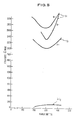
- Fig. 5 graphically illustrates the dependence of etch rate on power for silicon and silicon dioxide materials.
- the silicon etch rate is a nonlinear function of the power, exhibiting a high etch rate above about 150 watts and decreasing rapidly to zero as the power is reduced to zero.
- the trench has a positive slope.
- the slope becomes zero and then turns negative.
- the silicon dioxide etch rate graph is free of such variation indicating that the oxide etch rate is quite unaffected by the power.
- the ERR of silicon to silicon dioxide is high in the range 30-40:1; and the variation of the etch rate of silicon at a given power level with doping conditions is not significant indicating that the present novel process enables etching a silicon material of the type shown in Fig. 1 having doped layers 10, 12 and 14 to yield a substantially vertical profile.
- Figs. 6 and 7 are photographs made by a scanning electron microscope of a trench in silicon using the process conditions stipulated with regard to the Fig. 5 data.
- the negatively pitched trench shown in Fig. 6 was obtained using a power level of 400 watts.
- the positively pitched trench of Fig. 7 was obtained using a power of 200 watts. It is readily apparent from these figures that the silicon trench shape is amenable for change by using the four component gas mixture and merely manipulating the power employed for etching. Also, evident from Figs. 6 and 7 is that there is no black silicon (i.e., grass, cones, spikes, etc.) formation at the bottom of these 12 ⁇ m deep trenches.
- a silicon dioxide layer 46 is formed.
- the oxide 44 is a low temperature oxide (LTO) typically formed at a low temperature of about 400°C.
- LTO low temperature oxide
- the structure is subjected to the present etching process using the combination of fluorochlorohydrocarbon, SF6, O2 and an inert gas.
- the CCl2F2 + SF6 + O2 + He gas mixture is used in the same percentage rates as in the case of etching silicon described hereinabove.
- the plasma derived from this gas mixture facilitates etching the silicide 44 and polysilicon 42 into the conductor structures 48 with perfectly vertical walls 50. Since the etch rate of the oxide mask 42 is substantially low (nearly 30-40 times low) compared to that of layers 42 and 44 the integrity of the oxide mask is preserved and any undercutting beneath the mask is avoided.
- Figs. 8 and 9 are photographs made by scanning electron microscope of a LTO/TiSi2/polysilicon sandwich layer using the process of the present invention.
- Fig. 8 shows the sandwich structure in a cross-sectional view
- Fig. 9 shows a side view.
- the thickness of the LTO, TiSi2 and polysilicon were, respectively, 370nm, 200 nm and 370 nm.
- the etching was carried out under the following conditions: Flow rate He 54 sccm CCL2F2 4 SF6 2 O2 2.5 Pressure 55 mT Power 260 Watts Cathode size 40 cm
- the TiSi2 was etched at a rate of about 500 A/min. and the polysilicon was etched at a rate of about 800 A/min. obtaining a conductor structure with near vertical walls.
- the polysilicon etch rate was low compared to that shown in Fig. 5 because the silicon loading on the cathode surface (which affects the etch rate as illustrated in Fig. 10) was significantly higher than 12%.
- the RIE process comprised of a novel gas mixture of CCl2F2, SF6, O2 and He enables deep and narrow silicon trench etching.
- the resulting trenches have near perfect vertical walls, free of blooming, dove tailing, black silicon and other problems that plagued the prior art.
- the process is readily extendable to etching silicide and polyside layer patterning into fine line patterns.
- the process enables shape control of trenches by manipulating the RIE power. It is free of toxic and corrosive reaction components and suitable for use with a variety of RIE systems.
Abstract
Description
- This invention relates to a reactive ion etching (RIE) process for controllably etching semiconductor materials including silicon bulk and silicide and polycide films to obtain vertical wall profiles. More particularly, the invention is a RIE process characterized by good profile control, high etch selectivity to insulator masks and little toxicity and corrosiveness stemming from use of a novel combination of etchant gases.
- RIE is a well-known dry etching technique which finds extensive utility in the fabrication of semiconductor integrated circuits. A major application of RIE is to form deep trenches in a silicon substrate to surround an active or passive semiconductor device and electrically isolate the device. U.S. Pat. No. 4,104,086 issued to Bondur et al and assigned to the present assignee describes the details of the trench isolation process. The trenches are etched after masking portions of the substrate surface with a material (e.g., silicon dioxide or silicon nitride or a combination thereof) which has a lower etch rate than that of silicon. The trenches are then filled with a suitable material such as oxide, polyimide or polysilicon. Another major application of RIE is to define extremely narrow conductor lines (e.g., a gate for field effect transistor or interconnect structure for connecting devices on a substrate) from a deposited film of a refractory metal silicide, polycide (silicide/polysilicon sandwich), etc. In both these applications, it is imperative that the etched surfaces have substantially vertical profile and the (submicron) width of the trench/line be under tight control, lest severe constraints are imposed on the design and fabrication of viable and operable integrated circuits.
- A variety of etchant gases and their mixtures have been used in the prior art for RIE of semiconductors. U.S. Pat. No. 4,214,946 to Forget et al and assigned to the present assignee discloses use of a gas mixture consisting of 10 parts of SF6 and Cl₂ and the remainder an inert gas (He) for RIE of silicon or polysilicon. While this reference achieves an etch rate ratio (ERR) of Si:SiO2 exceeding 40:1, it is basically directed to etching shallow (about 0.5 µm depth) trenches. Moreover, this process has the fundamental disadvantages of high toxicity and corrossive power which necessitate highly expensive and complicated safety measures during etching. Another disadvantage is that additional process steps are required for making an etch mask of SiO₂ because photoresist etch masks cannot withstand these potent gases.
- U.S. Pat. No. 4,264,409 to Forget et al and assigned to the present assignee, discloses RIE of silicon or polysilcon using a gas mixture of SiF₄, Cl₂ and an inert gas (Ar or He). This process suffers from the same drawbacks as the afore mentioned '946 patent.
- U.S. Pat. No. 4,530,736 issued to Mutter and assigned to the present assignee discloses RIE of Si using 95-99% of CCl₃F or CCl₂F₂ in combination with 1-5% of oxygen using a photoresist mask. This patent teaches that oxygen is added to the other gas to increase the etch rate of the photoresist and oxygen does not have significant effect on the etch rate of silicon.
- U.S. Pat. No. 4,475,982 issued to Lai et al and assigned to the present assignee discloses RIE of deep trenches in silicon in an atmosphere of CCl₂F₂ and Ar to etch the lightly doped layers of silicon and CCl₂F₂ and oxygen to etch the heavily doped layers. The switch over to the second atmosphere is made to avoid lateral etching or "blooming" in the heavily doped layers of the silicon substrate.
- U.S. Pat. No. 3,880,684 issued to Abe et al describes a semiconductor prepared by continuously etching at least two types of silicon compound layers, such as, SiO₂, Si₃N₄ or polysilicon which are formed on a silicon substrate. A freon gas plasma is used for etching so that the two types of silicon compound layers are continuously etched in a sloped form with undercutting, as occurs in conventional wet chemical etching.
- The article entitled "Dry Process Technology (Reactive Ion Etching)" by J.A. Bondur, J. Vac. Sci. Tech.,
Vol 13, No. 5, pp. 1023-1029, Sept/Oct. 1976 discloses a variety of gases (CF₄, CCl₂F₂ - Freon 12, etc.) and gas combinations (CF₄+O2, CF₄+O2+He, etc.) for RIE of Si, SiO₂, Si₃N₄, etc. against a photoresist mask. Bondur concludes that even if the resist mask is square to the wafer surface, it does not insure that a vertical-walled image will result in the etched material since the plasma reacts with the photoresist. - U.S. Pat. No. 4,447,290 issued to Matthews teaches adding Freon 12 to an etchant gas mixture of SF₆ and oxygen during plasma etching of polysilicon on a Si₃N₄ layer for facilitating detection of the end point of polysilicon etching.
- U.S. Pat. No. 4,465,553 issued to Hijikata et al discloses patterning by etching silicon or a compound thereof using a gaseous mixture of SF₆ and C₂ClF₅.
- U.S. Pat. No. 4,473,435 issued to Zafiropoulo et al discloses plasma etching of a polysilicon film to expose a dielectric underlayer on a silicon substrate by using a gas mixture of SF₆ (or CF₄ or NF₃) and Freon (C₂ClF₅).
- U.S. Pat. No. 4,473,436 issued to Beinvogl discloses RIE of a polycide layer using a preferred gas mixture of SF₆ and Cl₂. The patentee states that "the invention can also be practiced by using gas mixtures which contain fluorohydrocarbons that are substituted with chlorine atoms (i.e. fluoro-chloro-carbons) such as CClF₃, CCl₂F₂ and mixtures thereof. Further, a carrier gas, preferably an inert gas, such as helium, can also be utilized in the practice of the invention".
- U.S. Pat. No. 4,330,384 issued to Okudaira et al discloses plasma etching of silicon with a gas mixture containing SF₆ and at least one of O₂, NH₃, N₂, CF₄ and CH₄.
- U.S. Pat. No. 4.455,193 issued to Jeuch et al discloses simultaneously etching photoresist and oxide layers using a mixture of CHF₃ (or CF₄) and O₂. Other disclosed etchant gases are SF₆ and a mixture of CF₄ and oxygen.
- U.S. Pat. No. 4,380,489 issued to Benivogl discloses plasma etching of polysilicon using SF₆ and He reactive gas mixture.
- U.S. Pat. No. 4,374,698 issued to Sanders et al discloses plasma etching a Si₃N₄ or SiO₂ layer using a gas mixture which contains a fluoride compound (CF₄ or CHF₃) and a compound which contains a halogen other than a fluoride (such as CF₂Cl₂).
- U.S. Pat. No. 4,589,952 issued to Behringer and assigned to the present assignee discloses RIE of deep trenches in silicon against a triple photoresist-Si₃N₄-photoresist mask using CF₄ etchant ambient containing a low fluorine concentration to obtain a substantially vertical trench wall profile.
- Despite the plethora of prior art on RIE etchant gas systems, there exists a strong need for an etchant gas chemistry which is capable of consistently and reliably providing deep and narrow silicon trenches with controlled wall profiles. A similar need exists with respect to patterning fine and ultrafine conductor lines with vertical surface profiles. These needs are particularly acute due to the insatiable demands imposed by the requirements of increased device density on a chip. Coupled to the chip density demands is the safety-at-workplace and environmental considerations making it imperative to avoid altogether any toxic or corrosive gas systems. The prior art gas systems which utilize Cl₂ as a component of the etchant gas fails to meet these requirements due to its inherent corrosive and toxic nature. The gas systems which do not use Cl₂ tend to be incapable of providing consistently and reliably controlled wall profiles. Unacceptable trench contour aberrations such as trench sidewall bowing are characteristic of these systems.
- Over and beyond the needs stipulated above, there exists a need to controllably alter the shape or pitch of isolation trenches to suit the particular trench-filling material and facilitate reliable trench isolation. For example, for filling trenches with an organic material such as polyimide, it is desirable to etch trenches having a negative pitch (i.e., the bottom of the trench is wider than the top) since, then, the organic will flow down along the trench surfaces and achieve capillary action to fill the trench without forming voids in the organic fill. While filling the trench with polysilicon, for example, a trench profile with a positive pitch (narrower at the bottom than at the top) is desired to prevent formation of large voids in the polysilicon-fill. The prior art failed to address these demands.
- Accordingly, it is an object of the invention to provide a process for etching a semiconductor material to obtain controllable wall profiles thereof.
- It is another object of the invention to provide an RIE gas system which has a high etch selectivity of a semiconductor against an insulator mask.
- It is a specific object of the invention to provide a RIE process for etching trenches in a semiconductor material by manipulating the composition of the component gases in the etchant gas system and/or the RIE process parameters.
- The above objects and other related objects may be achieved through the use of a novel etchant gas mixture composed of a fluoro-chloro-hydrocarbon, SF₆, oxygen and an inert gas such as helium. Suitable fluoro-chloro-carbon include CClF₃ (Freon 13), CCl₂F₂ (Freon 12), CCl₃F (Freon 11), CCl₄, the preferred fluoro-chloro-hydrocarbon being CCl₂F₂. The preferred proportion of the fluoro-chloro-hydrocarbon to SF₆ in the gas mixture is approximately 2. The etchant gas mixture being suitable for use, among others, with a single-or multi-wafer diode-configured parallel-plate RIE system, lends itself to etching deep and narrow trenches in a semiconductor substrate and patterning polycide, silicide and other films into fine lines having substantially vertical wall profiles. In the trench definition context, the gas mixture permits shape control of the trench (to provide a positive, negative or zero pitch to the trench) by mere control of the RF power applied to the RIE system while strictly maintaining the width of the opening in the trench-definition mask. The presence of the oxygen facilitates a high ERR of semiconductor material to the insulator mask by decreasing the etch rate of the insulator. For example, ERR of Si:SiO₂ = 30-40:1.
- The novel process steps and their combination characteristic of the invention are set forth in the appended claims. The invention itself, however, will be best understood by reference to the detailed description which follows in conjunction with the accompanying drawings, wherein:
- Fig. 1 illustrates in cross-sectional representation RIE of silicon in accordance with the present process to form deep trenches having vertical walls and a width identical to that of the opening in the RIE mask.
- Figs. 2 and 3 illustrate in cross-sectional representation RIE of silicon in accordance with the invention to form deep trenches of varying shape (positive and negative pitch, respectively) by varying the power for generating the RIE species.
- Fig. 4 illustrates in cross-sectional representation RIE patterning of a polycide layer in accordance with the present invention into conductors having well-defined and vertical wall profile.
- Fig. 5 is a graphical illustration of the dependence of etch rate of polysilicon and oxide on power.
- Figs. 6 and 7 are photographs made by scanning electron microscopy of trenches formed in silicon using the process of the present invention by merely changing the power.
- Figs. 8 and 9 are photographs made by scanning electron microscopy of polycide lines etched from a polycide film using the novel etchant gas system of the invention.
- Fig. 10 is a graphical illustration of the effect of silicon loading on etch rate of silicon and silicon dioxide.
- The invention can be practiced using any of the RIE systems well-known in the art. One such RIE system is disclosed in U.S. patent no. 4,595,484 issued to Giammarco et al and assigned to the present assignee. This patent is hereby incorporated by reference herein. Since such a system is not the subject of the present invention, the detailed description will focus on the novel RIE method utilizing a novel gas mixture rather than on the RIE system.
- Referring now particularly to Fig. 1, the RIE for one form of the present invention for forming dielectric trench isolation is shown. The structure of Fig. 1 includes a
monocrystalline silicon substrate 10 which is shown as P+ conductivity for purposes of illustration, anN+ layer 12 over thesubstrate 10 and an N-conductivity layer 14 on thelayer 12. For purposes of the invention, either all or some of thelayers 10. 12 and 14 could be of opposite conductivity from the conductivity type indicated. However, it is preferred to have thelayer 12 to be in a conductivity region where it will ultimately be the collector of a bipolar transistor. The structure can be fabricated by various well-known techniques. However, the preferred technique is to provide a monocrystalline silicon substrate and to diffuse an N+ blanket diffusion into the substrate by using conventional diffusion or ion implantation of an N type impurity such as arsenic, antimony or phosphorus to produce an Nregion with a surface concentration of between about 1019 and 1021 atoms/cc. Thelayer 14 is subsequently grown on to the 10-12 structure by means of an epitaxial growth. This may be done by conventional techniques such as use of SiCl₄/H₂ or SiH₄/H₂ mixtures at growth temperatures of about 1000°C.The N+ layer 12 may have a typical thickness of about 1-3 µm whereas the epitaxial layer has a thickness of about 0.5-10 µm, the exact thicknesses being depending on the device to be built. - Next, a
silicon dioxide layer 16 is formed by conventional techniques of either thermal growth at a temperature of about 950°C in a wet or dry oxygen ambient or by chemical vapor deposition. Other mask materials may also be used such as silicon nitride and aluminum oxide.Openings 18 having a width W are formed in theoxide 16 in the regions where dielectric isolation is desired. These openings are formed by the conventional photolithography and etching techniques. The thickness of maskinglayer 16 is about 0.2-2 µm, the exact thickness depending on the depth requirement of the silicon trench. - The structure is now ready for the reactive ion etching process, per the invention. This process may be more fully understood with reference to the afore-mentioned Giammarco et al patent which contains a full description of the RIE apparatus. The substrate structure 10-12-14-16 shown in Fig. 1 is mounted on the cathode plate of the RIE apparatus. After proper evacuation of the reaction chamber, an etchant gas mixture consisting of a fluorochlorohydrocarbon, SF₆, oxygen and an inert gas is introduced into the chamber. The preferred fluorochlorocarbon gas is CCl₂F₂ (Freon 12) and the preferred inert gas is He. If w designates the percentage of the helium gas, x designates the percent of Freon-12, y designates that of SF₆ and z designates the percentage of oxygen gas in the etchant gas mixture, the sum total of w, x, y and z should be about 100. Additionally, best control of the etching process is obtained when Freon-12 is about twice as much as SF₆ in the gas mixture, i.e., when x/y = 2. The preferred gas mixture which would facilitate a high etch rate ratio of semiconductor to insulator while providing excellent controllability of the etching process has a Freon-12 content of about 3%-10%, SF₆ of about 1%-4%, O₂ of about 3%-10% and He content of about 74%-93%.
- The component gases of the etchant gas mixture are introduced into the RIE system via the inlet port thereof using individual flow controllers external to the inlet port. By controlling the flow rate of the component gases, the percent content of the gases in the mixture is controlled. Since the distance between the flow controllers and the reaction volume is substantially large, the component gases mix homogeneously prior to diffusion into the reaction volume. The pressure in the chamber is maintained independently by a throttle valve at the chamber outlet. The flow rates and the pumping speed are adjusted such that the etchant gas mixture remains in the process chamber for an optimum period of time to balance the buildup and decline of the active species which are responsible for etching, but not so long that the byproducts of the reaction seriously inhibit the reaction. A chamber pressure of below about 100 millitorr is typically used and the flow rates of the etchant gas are adjusted to obtain the previously mentioned composition ranges.
- Radiofrequency (RF) power is applied to the substrate-mounting plate to effectively negative bias this plate with respect to the anode. An RF on the order of 13.56 MHz delivering a suitable power is used. The power level is dictated, to a degree, by the size of the cathode plate. For a 16-inch diameter plate, a power of about 200-400 watts or a power density of about 0.1-0.4 watt/sq cm is typically used.
- Under these conditions the silicon substrate 14-12-10 (Fig. 1) is etched against the
RIE mask 16 to form a deep andnarrow trench 20 having substantiallyvertical walls 22. The ERR of silicon to oxide is high, about 30-40:1. This high ERR avoids any erosion and lifting of theoxide mask 16, thereby facilitating excellent control over theopening 18 in the mask. The wall profile is vertical over the entire depth of the trench regardless of the doping profile or type of dopant incorporated into the substrate, as illustrated in Fig. 1. Since the wall profile is vertical, the width of the trench will be substantially the same as the width W of theopening 18 in themask 16. - It is not clear what specific mechanism gives rise to the high ERR and vertical wall profile. However, oxygen, despite its low content in the etchant gas mixture, is a necessary and key ingredient of the etchant gas mixture responsible for the high ERR. A plausible explanation for the vertical wall profile is as follows. The RF field generates the etchant species by suitably breaking up the molecules of the etchant gas. The Freon gas provides a species which passivates the vertical surfaces of silicon preventing lateral etching thereof by radicals in the etchant gas responsible for etching. In other words, Freon provides "Cl" species which are chemisorbed onto the silicon trench surfaces forming a barrier on the surfaces preventing or "protecting" the vertical surfaces from any significant etching. Simultaneously, "F" radicals supplied by Freon and SF₆ molecules in the etchant gas, by virtue of their high momentum in a substantially vertical direction gained from the RF field and ability to chemically interact with the silicon, react spontaneously with the horizontal surface of the trench causing etching in a vertical direction. The vertical etch rate is a function of the RF power applied to the structure 14-12-10. As the power is increased, the etch rate is correspondingly increased due to the increased energy imparted to the etching species. The increased energy results in increased temperature of the substrate. It is believed that increased temperature of the substrate causes the trench to widen at the bottom as RF power is increased. The increase in thermal energy causes the sidewall passivation to diminish, so lateral etching will occur.
- The unique four-component etchant gas mixture has the advantageous feature of image shape control. As illustrated in Figs. 2 and 3, utilizing this gas mixture, the shape of the trench can be conveniently altered to have a negative or positive pitch by merely changing the power density of the RIE system. By increasing the power density from that used to obtain the substantially vertical trench profile illustrated in Fig. 1, a
trench 24 having a negative pitch as indicated in Fig. 2 may be obtained. Thesidewalls 26 of thetrench 24 are outwardly sloped. Likewise, by decreasing the power density of the RIE system below that used for obtaining the wall profile of trench 20 (Fig. 1), atrench 28 having a positive pitch comprised of inwardly slopedwalls 30 is obtained. As indicated in Figs. 2 and 3, variation of RIE system power, however, has little effect on the width W of the opening in theoxide mask 18. This is particularly advantageous from a circuit design standpoint since the width of the trench at the top corresponds exactly to that defined by lithography. - The above trench shape control may be understood by reference to Fig. 5 which graphically illustrates the dependence of etch rate on power for silicon and silicon dioxide materials. The data corresponds to the following etching conditions: pressure = 75 mT; flow rates (and the equivalent percent content) of the component gases are 55 sccm (or 86%) of He, 4 sccm (or 6.25%) of CCl₂F₂, 3 sccm (or 4.7%) of SF₆ and 2 sccm (or 3.15%) of O₂; silicon load of 12%; the diameter of the cathode plate was about 40 cm; temperature of cathode plate is room temperature. The silicon etch rate is a nonlinear function of the power, exhibiting a high etch rate above about 150 watts and decreasing rapidly to zero as the power is reduced to zero. At a power setting of about 200 watts, the trench has a positive slope. At higher power levels, the slope becomes zero and then turns negative. The silicon dioxide etch rate graph, on the other hand, is free of such variation indicating that the oxide etch rate is quite unaffected by the power. Also evident from Fig. 5 is that the ERR of silicon to silicon dioxide is high in the range 30-40:1; and the variation of the etch rate of silicon at a given power level with doping conditions is not significant indicating that the present novel process enables etching a silicon material of the type shown in Fig. 1 having doped
layers - Dramatic results of the above graphical data is shown in Figs. 6 and 7 which are photographs made by a scanning electron microscope of a trench in silicon using the process conditions stipulated with regard to the Fig. 5 data. The negatively pitched trench shown in Fig. 6 was obtained using a power level of 400 watts. The positively pitched trench of Fig. 7 was obtained using a power of 200 watts. It is readily apparent from these figures that the silicon trench shape is amenable for change by using the four component gas mixture and merely manipulating the power employed for etching. Also, evident from Figs. 6 and 7 is that there is no black silicon (i.e., grass, cones, spikes, etc.) formation at the bottom of these 12 µm deep trenches.
- Equally impressive results are obtained in accordance with the present process while patterning silicide and polycide layers by etching into fine lines. This is illustrated in Fig. 4. Starting with a silicon substrate having a 200-400 nm thick doped or
undoped polysilicon layer 42, 150-300 nm thick refractory metal silicide (e.g., TiSi₂, TaSi₂ or WSi₂) layer 44, asilicon dioxide layer 46 is formed. The oxide 44 is a low temperature oxide (LTO) typically formed at a low temperature of about 400°C. Using conventional photolithography and etching using 100% CF₄ plasma, theoxide layer 46 is patterned into a configuration desired of the underlying polycide 42-44. Once the oxide is patterned into a RIE mask for the polycide layer, the structure is subjected to the present etching process using the combination of fluorochlorohydrocarbon, SF₆, O₂ and an inert gas. In a preferred embodiment, the CCl₂F₂ + SF₆ + O₂ + He gas mixture is used in the same percentage rates as in the case of etching silicon described hereinabove. Under suitable power density the plasma derived from this gas mixture facilitates etching the silicide 44 andpolysilicon 42 into theconductor structures 48 with perfectlyvertical walls 50. Since the etch rate of theoxide mask 42 is substantially low (nearly 30-40 times low) compared to that oflayers 42 and 44 the integrity of the oxide mask is preserved and any undercutting beneath the mask is avoided. - Figs. 8 and 9 are photographs made by scanning electron microscope of a LTO/TiSi₂/polysilicon sandwich layer using the process of the present invention. Fig. 8 shows the sandwich structure in a cross-sectional view and Fig. 9 shows a side view. The thickness of the LTO, TiSi₂ and polysilicon were, respectively, 370nm, 200 nm and 370 nm. The etching was carried out under the following conditions:
Flow rate He 54 sccm
CCL₂F₂ 4
SF₆ 2
O₂ 2.5
Pressure 55 mT
Power 260 Watts
Cathode size 40 cm
- Under these conditions, the TiSi₂ was etched at a rate of about 500 A/min. and the polysilicon was etched at a rate of about 800 A/min. obtaining a conductor structure with near vertical walls. The polysilicon etch rate was low compared to that shown in Fig. 5 because the silicon loading on the cathode surface (which affects the etch rate as illustrated in Fig. 10) was significantly higher than 12%.
- In summary, the RIE process comprised of a novel gas mixture of CCl₂F₂, SF₆, O₂ and He enables deep and narrow silicon trench etching. The resulting trenches have near perfect vertical walls, free of blooming, dove tailing, black silicon and other problems that plagued the prior art. The process is readily extendable to etching silicide and polyside layer patterning into fine line patterns. The process enables shape control of trenches by manipulating the RIE power. It is free of toxic and corrosive reaction components and suitable for use with a variety of RIE systems.
- Thus, there has been described in accordance with the invention a RIE process that fully satisfies the objects and advantages set forth above.
- While the invention has been described in conjunction with specific preferred embodiments, it is evident that many alternatives, modifications and variations will be apparent to those skilled in the art in light of the foregoing description. It is therefore contemplated that the appended claims will embrace any such alternatives, modifications and variations as fall within the scope and spirit of the invention.
Claims (22)
providing a semiconductor material having an inorganic material mask thereon; and
subjecting said material to a plasma consisting of w percent inert gas, x percent fluorochlorocarbon, y percent SF₆ and z percent O₂ wherein w+x+y+z is 100% and each of said w,x,y and z percentage exceeds 0%.
providing a semiconductor material having an inorganic material mask thereon; and
subjecting said material to an RF plasma consisting essentially of w percent of an inert gas, x percent of a fluorochlorocarbon, y percent of SF₆ and z percent of O₂ where said w,x,y and z is each greater than zero and w+x+y+z is essentially one hundred percent to etch the regions of said material not masked by said mask.
providing a metal silicide and polysilicon dual layer having an inorganic mask thereon; and
subjecting said layer to a plasma composed of CCl₂F₂, He, O₂ and SF₆.
Applications Claiming Priority (2)
| Application Number | Priority Date | Filing Date | Title |
|---|---|---|---|
| US904437 | 1986-08-09 | ||
| US06/904,437 US4726879A (en) | 1986-09-08 | 1986-09-08 | RIE process for etching silicon isolation trenches and polycides with vertical surfaces |
Publications (3)
| Publication Number | Publication Date |
|---|---|
| EP0256311A2 true EP0256311A2 (en) | 1988-02-24 |
| EP0256311A3 EP0256311A3 (en) | 1990-07-25 |
| EP0256311B1 EP0256311B1 (en) | 1993-02-10 |
Family
ID=25419165
Family Applications (1)
| Application Number | Title | Priority Date | Filing Date |
|---|---|---|---|
| EP87110157A Expired - Lifetime EP0256311B1 (en) | 1986-08-09 | 1987-07-14 | Rie process for etching silicon isolation trenches and polycides with vertical surfaces |
Country Status (4)
| Country | Link |
|---|---|
| US (1) | US4726879A (en) |
| EP (1) | EP0256311B1 (en) |
| JP (1) | JPH0744175B2 (en) |
| DE (1) | DE3784117T2 (en) |
Cited By (8)
| Publication number | Priority date | Publication date | Assignee | Title |
|---|---|---|---|---|
| EP0317794A2 (en) * | 1987-11-23 | 1989-05-31 | International Business Machines Corporation | Chlorofluorocarbon additives for enhancing etch rates in fluorinated halocarbon/oxidant plasmas |
| EP0504758A2 (en) * | 1991-03-19 | 1992-09-23 | Tokyo Electron Limited | Plasma etching method fo silicon containing layer |
| DE4219592A1 (en) * | 1991-06-17 | 1992-12-24 | Gold Star Electronics | Dielectric insulation filled trenches prodn. in semiconductor substrate - using localised reaction substrate with deposited metal layer and removal of the prod., then filling trenches and planarising |
| DE4416057A1 (en) * | 1994-05-02 | 1995-11-09 | Mannesmann Ag | Prodn. of three=dimensional structures in silicon substrates |
| US5560804A (en) * | 1991-03-19 | 1996-10-01 | Tokyo Electron Limited | Etching method for silicon containing layer |
| GB2335795A (en) * | 1998-03-27 | 1999-09-29 | Nec Corp | Etching or depositing films on substrates |
| EP1763074A2 (en) | 2005-09-09 | 2007-03-14 | Infineon Technologies AG | Isolation for Semiconductor Devices |
| KR20190142272A (en) * | 2018-06-15 | 2019-12-26 | 타이완 세미콘덕터 매뉴팩쳐링 컴퍼니 리미티드 | Negatively sloped isolation structures |
Families Citing this family (53)
| Publication number | Priority date | Publication date | Assignee | Title |
|---|---|---|---|---|
| JPS6432627A (en) * | 1987-07-29 | 1989-02-02 | Hitachi Ltd | Low-temperature dry etching method |
| JPS6432633A (en) * | 1987-07-29 | 1989-02-02 | Hitachi Ltd | Taper etching method |
| JP2624797B2 (en) * | 1988-09-20 | 1997-06-25 | 株式会社日立製作所 | Active matrix substrate manufacturing method |
| US5064165A (en) * | 1989-04-07 | 1991-11-12 | Ic Sensors, Inc. | Semiconductor transducer or actuator utilizing corrugated supports |
| JP2883629B2 (en) * | 1989-04-21 | 1999-04-19 | 富士電機 株式会社 | Dry etching method and dry etching apparatus |
| US5271799A (en) * | 1989-07-20 | 1993-12-21 | Micron Technology, Inc. | Anisotropic etch method |
| US5201993A (en) * | 1989-07-20 | 1993-04-13 | Micron Technology, Inc. | Anisotropic etch method |
| US5300460A (en) * | 1989-10-03 | 1994-04-05 | Applied Materials, Inc. | UHF/VHF plasma for use in forming integrated circuit structures on semiconductor wafers |
| US5015323A (en) * | 1989-10-10 | 1991-05-14 | The United States Of America As Represented By The Secretary Of Commerce | Multi-tipped field-emission tool for nanostructure fabrication |
| US5225376A (en) * | 1990-05-02 | 1993-07-06 | Nec Electronics, Inc. | Polysilicon taper process using spin-on glass |
| US5068707A (en) * | 1990-05-02 | 1991-11-26 | Nec Electronics Inc. | DRAM memory cell with tapered capacitor electrodes |
| US5169487A (en) * | 1990-08-27 | 1992-12-08 | Micron Technology, Inc. | Anisotropic etch method |
| JP3729869B2 (en) * | 1990-09-28 | 2005-12-21 | セイコーエプソン株式会社 | Manufacturing method of semiconductor device |
| US5094712A (en) * | 1990-10-09 | 1992-03-10 | Micron Technology, Inc. | One chamber in-situ etch process for oxide and conductive material |
| US5888414A (en) * | 1991-06-27 | 1999-03-30 | Applied Materials, Inc. | Plasma reactor and processes using RF inductive coupling and scavenger temperature control |
| US5358601A (en) * | 1991-09-24 | 1994-10-25 | Micron Technology, Inc. | Process for isotropically etching semiconductor devices |
| DE4228551C2 (en) * | 1992-08-27 | 1996-02-22 | Linde Ag | Method and application of the method for the cleaning treatment of surfaces with a low pressure plasma |
| DE4232475C2 (en) * | 1992-09-28 | 1998-07-02 | Siemens Ag | Process for plasma chemical dry etching of Si¶3¶N¶4¶ layers highly selective to SiO¶2¶ layers |
| US5770098A (en) * | 1993-03-19 | 1998-06-23 | Tokyo Electron Kabushiki Kaisha | Etching process |
| US5354417A (en) * | 1993-10-13 | 1994-10-11 | Applied Materials, Inc. | Etching MoSi2 using SF6, HBr and O2 |
| JP3351183B2 (en) * | 1995-06-19 | 2002-11-25 | 株式会社デンソー | Dry etching method and trench forming method for silicon substrate |
| US5652170A (en) | 1996-01-22 | 1997-07-29 | Micron Technology, Inc. | Method for etching sloped contact openings in polysilicon |
| JP2956602B2 (en) * | 1996-08-26 | 1999-10-04 | 日本電気株式会社 | Dry etching method |
| US5914280A (en) * | 1996-12-23 | 1999-06-22 | Harris Corporation | Deep trench etch on bonded silicon wafer |
| US6127278A (en) * | 1997-06-02 | 2000-10-03 | Applied Materials, Inc. | Etch process for forming high aspect ratio trenched in silicon |
| US5891807A (en) * | 1997-09-25 | 1999-04-06 | Siemens Aktiengesellschaft | Formation of a bottle shaped trench |
| US5935874A (en) * | 1998-03-31 | 1999-08-10 | Lam Research Corporation | Techniques for forming trenches in a silicon layer of a substrate in a high density plasma processing system |
| US6103585A (en) * | 1998-06-09 | 2000-08-15 | Siemens Aktiengesellschaft | Method of forming deep trench capacitors |
| TW398053B (en) * | 1998-07-31 | 2000-07-11 | United Microelectronics Corp | Manufacturing of shallow trench isolation |
| US6312616B1 (en) | 1998-12-03 | 2001-11-06 | Applied Materials, Inc. | Plasma etching of polysilicon using fluorinated gas mixtures |
| US6583063B1 (en) | 1998-12-03 | 2003-06-24 | Applied Materials, Inc. | Plasma etching of silicon using fluorinated gas mixtures |
| US6235214B1 (en) | 1998-12-03 | 2001-05-22 | Applied Materials, Inc. | Plasma etching of silicon using fluorinated gas mixtures |
| US6191043B1 (en) | 1999-04-20 | 2001-02-20 | Lam Research Corporation | Mechanism for etching a silicon layer in a plasma processing chamber to form deep openings |
| DE19919469A1 (en) | 1999-04-29 | 2000-11-02 | Bosch Gmbh Robert | Process for plasma etching silicon |
| US6355567B1 (en) * | 1999-06-30 | 2002-03-12 | International Business Machines Corporation | Retrograde openings in thin films |
| US6270634B1 (en) | 1999-10-29 | 2001-08-07 | Applied Materials, Inc. | Method for plasma etching at a high etch rate |
| US6221784B1 (en) | 1999-11-29 | 2001-04-24 | Applied Materials Inc. | Method and apparatus for sequentially etching a wafer using anisotropic and isotropic etching |
| US6391790B1 (en) | 2000-05-22 | 2002-05-21 | Applied Materials, Inc. | Method and apparatus for etching photomasks |
| US7115523B2 (en) * | 2000-05-22 | 2006-10-03 | Applied Materials, Inc. | Method and apparatus for etching photomasks |
| US6544838B2 (en) | 2001-03-13 | 2003-04-08 | Infineon Technologies Ag | Method of deep trench formation with improved profile control and surface area |
| DE10127888A1 (en) * | 2001-06-08 | 2002-12-19 | Infineon Technologies Ag | Process for forming contact holes in contact regions of components integrated in a substrate comprises applying an insulating layer on a substrate with the integrated components, and applying a mask with openings |
| US7183201B2 (en) | 2001-07-23 | 2007-02-27 | Applied Materials, Inc. | Selective etching of organosilicate films over silicon oxide stop etch layers |
| US6955989B2 (en) * | 2001-11-30 | 2005-10-18 | Xerox Corporation | Use of a U-groove as an alternative to using a V-groove for protection against dicing induced damage in silicon |
| KR20040012451A (en) * | 2002-05-14 | 2004-02-11 | 어플라이드 머티어리얼스, 인코포레이티드 | Methods for etching photolithographic reticles |
| KR100529632B1 (en) * | 2003-10-01 | 2005-11-17 | 동부아남반도체 주식회사 | Semiconductor device and fabrication method thereof |
| TWI249767B (en) * | 2004-02-17 | 2006-02-21 | Sanyo Electric Co | Method for making a semiconductor device |
| US7262110B2 (en) * | 2004-08-23 | 2007-08-28 | Micron Technology, Inc. | Trench isolation structure and method of formation |
| US8293430B2 (en) * | 2005-01-27 | 2012-10-23 | Applied Materials, Inc. | Method for etching a molybdenum layer suitable for photomask fabrication |
| DE102005053494A1 (en) * | 2005-11-09 | 2007-05-16 | Fraunhofer Ges Forschung | Process for producing electrically conductive feedthroughs through non-conductive or semiconductive substrates |
| JP2010272758A (en) * | 2009-05-22 | 2010-12-02 | Hitachi High-Technologies Corp | Plasma etching method for etching object |
| US8680607B2 (en) * | 2011-06-20 | 2014-03-25 | Maxpower Semiconductor, Inc. | Trench gated power device with multiple trench width and its fabrication process |
| US20130043559A1 (en) * | 2011-08-17 | 2013-02-21 | International Business Machines Corporation | Trench formation in substrate |
| CN103197376B (en) * | 2013-02-06 | 2015-05-13 | 上海交通大学 | Silicon waveguide preparation method based on polycrystalline silicon mask |
Citations (5)
| Publication number | Priority date | Publication date | Assignee | Title |
|---|---|---|---|---|
| EP0015403A1 (en) * | 1979-02-21 | 1980-09-17 | International Business Machines Corporation | Process for reactive ion-etching of silicon |
| EP0094528A2 (en) * | 1982-05-05 | 1983-11-23 | Siemens Aktiengesellschaft | Process for producing double-layer structures consisting of metal silicide and polysilicium on substrates containing integrated circuits by reactive ion etching |
| US4595484A (en) * | 1985-12-02 | 1986-06-17 | International Business Machines Corporation | Reactive ion etching apparatus |
| JPS6229141A (en) * | 1985-07-31 | 1987-02-07 | Hitachi Ltd | Manufacture of semiconductor device |
| EP0146446B1 (en) * | 1983-11-17 | 1989-11-08 | ETAT FRANCAIS représenté par le Ministre des PTT (Centre National d'Etudes des Télécommunications) | Process and apparatus for plasma treatment of semiconductor materials |
Family Cites Families (16)
| Publication number | Priority date | Publication date | Assignee | Title |
|---|---|---|---|---|
| US3880684A (en) * | 1973-08-03 | 1975-04-29 | Mitsubishi Electric Corp | Process for preparing semiconductor |
| US4104086A (en) * | 1977-08-15 | 1978-08-01 | International Business Machines Corporation | Method for forming isolated regions of silicon utilizing reactive ion etching |
| US4330384A (en) * | 1978-10-27 | 1982-05-18 | Hitachi, Ltd. | Process for plasma etching |
| US4264409A (en) * | 1980-03-17 | 1981-04-28 | International Business Machines Corporation | Contamination-free selective reactive ion etching or polycrystalline silicon against silicon dioxide |
| NL8004005A (en) * | 1980-07-11 | 1982-02-01 | Philips Nv | METHOD FOR MANUFACTURING A SEMICONDUCTOR DEVICE |
| DE3103177A1 (en) * | 1981-01-30 | 1982-08-26 | Siemens AG, 1000 Berlin und 8000 München | METHOD FOR PRODUCING POLYSILIZIUM STRUCTURES UP TO THE 1 (MY) M AREA ON SUBSTRATES CONTAINING INTEGRATED SEMICONDUCTOR CIRCUITS BY PLASMA |
| US4353777A (en) * | 1981-04-20 | 1982-10-12 | Lfe Corporation | Selective plasma polysilicon etching |
| US4447290A (en) * | 1982-06-10 | 1984-05-08 | Intel Corporation | CMOS Process with unique plasma etching step |
| FR2529714A1 (en) * | 1982-07-01 | 1984-01-06 | Commissariat Energie Atomique | METHOD FOR PRODUCING THE FIELD OXIDE OF AN INTEGRATED CIRCUIT |
| EP0098318B1 (en) * | 1982-07-03 | 1987-02-11 | Ibm Deutschland Gmbh | Process for the formation of grooves having essentially vertical lateral silicium walls by reactive ion etching |
| DE3242113A1 (en) * | 1982-11-13 | 1984-05-24 | Ibm Deutschland Gmbh, 7000 Stuttgart | METHOD FOR PRODUCING A THIN DIELECTRIC INSULATION IN A SILICON SEMICONDUCTOR BODY |
| JPS5993880A (en) * | 1982-11-20 | 1984-05-30 | Tokyo Denshi Kagaku Kabushiki | Dry etching method |
| US4473435A (en) * | 1983-03-23 | 1984-09-25 | Drytek | Plasma etchant mixture |
| US4530736A (en) * | 1983-11-03 | 1985-07-23 | International Business Machines Corporation | Method for manufacturing Fresnel phase reversal plate lenses |
| JPS60109234A (en) * | 1983-11-18 | 1985-06-14 | Nippon Telegr & Teleph Corp <Ntt> | Method for etching process of two-layer film |
| US4475982A (en) * | 1983-12-12 | 1984-10-09 | International Business Machines Corporation | Deep trench etching process using CCl2 F2 /Ar and CCl2 F.sub. /O2 RIE |
-
1986
- 1986-09-08 US US06/904,437 patent/US4726879A/en not_active Expired - Fee Related
-
1987
- 1987-07-14 EP EP87110157A patent/EP0256311B1/en not_active Expired - Lifetime
- 1987-07-14 DE DE8787110157T patent/DE3784117T2/en not_active Expired - Fee Related
- 1987-07-15 JP JP62175036A patent/JPH0744175B2/en not_active Expired - Lifetime
Patent Citations (5)
| Publication number | Priority date | Publication date | Assignee | Title |
|---|---|---|---|---|
| EP0015403A1 (en) * | 1979-02-21 | 1980-09-17 | International Business Machines Corporation | Process for reactive ion-etching of silicon |
| EP0094528A2 (en) * | 1982-05-05 | 1983-11-23 | Siemens Aktiengesellschaft | Process for producing double-layer structures consisting of metal silicide and polysilicium on substrates containing integrated circuits by reactive ion etching |
| EP0146446B1 (en) * | 1983-11-17 | 1989-11-08 | ETAT FRANCAIS représenté par le Ministre des PTT (Centre National d'Etudes des Télécommunications) | Process and apparatus for plasma treatment of semiconductor materials |
| JPS6229141A (en) * | 1985-07-31 | 1987-02-07 | Hitachi Ltd | Manufacture of semiconductor device |
| US4595484A (en) * | 1985-12-02 | 1986-06-17 | International Business Machines Corporation | Reactive ion etching apparatus |
Non-Patent Citations (5)
| Title |
|---|
| JOURNAL ELECTROCHEMICAL SOCIETY vol. 129, no. 11, November 1982, pages 2541-2547; C.B. Zarowin et al.: "Control of Plasma Etch Profiles with Plasma Sheath Electric Field and RF Power density" pages 2542-2544 * |
| JOURNAL ELECTROCHEMICAL SOCIETY. vol. 129, no. 11, November 1982, pages 2541-2547; C.B. ZAROWIN et al.: "Control of Plasma Etch Profiles with Plasma Sheath Electric Field and RF Power Density". * |
| PATENT ABSTRACTS OF JAPAN. vol. 11, no. 204, (E-520) 2nd July 1987; & JP-A-62 029 141 (HITACHI LTD) 07-02-1987 * |
| PROCEEDINGS OF THE 2ND INTERNATIONAL IEEE VLSI MULTILEVEL INTERCONNECTION CONFERENCE 25-26th June 1985, pages 301-306, Santa Clara CA; US G.C. CHERN et al.: "Anisotropic Tungsten Polcyide Plasma Etching" pages 303.304; * |
| PROCEEDINGS OF THE 2ND INTERNATIONAL IEEE VLSI MULTILEVEL INTERCONNECTION CONFERENCE. 25-26th June 1985, pages 301-306, Santa Clara CA, US; G.C. CHERN et al.: "Anisotropic Tungsten Polycide Plasma Etching". * |
Cited By (15)
| Publication number | Priority date | Publication date | Assignee | Title |
|---|---|---|---|---|
| EP0317794A3 (en) * | 1987-11-23 | 1989-07-05 | International Business Machines Corporation | Chlorofluorocarbon additives for enhancing etch rates in fluorinated halocarbon/oxidant plasmas |
| EP0317794A2 (en) * | 1987-11-23 | 1989-05-31 | International Business Machines Corporation | Chlorofluorocarbon additives for enhancing etch rates in fluorinated halocarbon/oxidant plasmas |
| US5560804A (en) * | 1991-03-19 | 1996-10-01 | Tokyo Electron Limited | Etching method for silicon containing layer |
| EP0504758A2 (en) * | 1991-03-19 | 1992-09-23 | Tokyo Electron Limited | Plasma etching method fo silicon containing layer |
| EP0504758A3 (en) * | 1991-03-19 | 1993-06-09 | Tokyo Electron Limited | Plasma etching method fo silicon containing layer |
| DE4219592A1 (en) * | 1991-06-17 | 1992-12-24 | Gold Star Electronics | Dielectric insulation filled trenches prodn. in semiconductor substrate - using localised reaction substrate with deposited metal layer and removal of the prod., then filling trenches and planarising |
| DE4219592C2 (en) * | 1991-06-17 | 2001-12-06 | Gold Star Electronics | Method for forming a trench isolation region using a reaction layer |
| DE4416057A1 (en) * | 1994-05-02 | 1995-11-09 | Mannesmann Ag | Prodn. of three=dimensional structures in silicon substrates |
| DE4416057C2 (en) * | 1994-05-02 | 1998-12-03 | Hartmann & Braun Gmbh & Co Kg | Process for the production of three-dimensional deep structures in silicon substrates |
| GB2335795A (en) * | 1998-03-27 | 1999-09-29 | Nec Corp | Etching or depositing films on substrates |
| US6177147B1 (en) | 1998-03-27 | 2001-01-23 | Nec Corporation | Process and apparatus for treating a substrate |
| GB2335795B (en) * | 1998-03-27 | 2003-03-12 | Nec Corp | Process and apparatus for treating a substrate |
| EP1763074A2 (en) | 2005-09-09 | 2007-03-14 | Infineon Technologies AG | Isolation for Semiconductor Devices |
| EP1763074A3 (en) * | 2005-09-09 | 2011-06-01 | Infineon Technologies AG | Isolation for Semiconductor Devices |
| KR20190142272A (en) * | 2018-06-15 | 2019-12-26 | 타이완 세미콘덕터 매뉴팩쳐링 컴퍼니 리미티드 | Negatively sloped isolation structures |
Also Published As
| Publication number | Publication date |
|---|---|
| JPS6365625A (en) | 1988-03-24 |
| US4726879A (en) | 1988-02-23 |
| DE3784117T2 (en) | 1993-08-12 |
| DE3784117D1 (en) | 1993-03-25 |
| EP0256311A3 (en) | 1990-07-25 |
| EP0256311B1 (en) | 1993-02-10 |
| JPH0744175B2 (en) | 1995-05-15 |
Similar Documents
| Publication | Publication Date | Title |
|---|---|---|
| EP0256311B1 (en) | Rie process for etching silicon isolation trenches and polycides with vertical surfaces | |
| US7049244B2 (en) | Method for enhancing silicon dioxide to silicon nitride selectivity | |
| US6069091A (en) | In-situ sequential silicon containing hard mask layer/silicon layer plasma etch method | |
| US5286344A (en) | Process for selectively etching a layer of silicon dioxide on an underlying stop layer of silicon nitride | |
| US5843226A (en) | Etch process for single crystal silicon | |
| US4528066A (en) | Selective anisotropic reactive ion etching process for polysilicide composite structures | |
| US6461976B1 (en) | Anisotropic etch method | |
| US5007982A (en) | Reactive ion etching of silicon with hydrogen bromide | |
| US4473436A (en) | Method of producing structures from double layers of metal silicide and polysilicon on integrated circuit substrates by RIE utilizing SF6 and Cl2 | |
| US6756313B2 (en) | Method of etching silicon nitride spacers with high selectivity relative to oxide in a high density plasma chamber | |
| US8133817B2 (en) | Shallow trench isolation etch process | |
| US20060011579A1 (en) | Gas compositions | |
| US5354421A (en) | Dry etching method | |
| US6670265B2 (en) | Low K dielectic etch in high density plasma etcher | |
| US4654112A (en) | Oxide etch | |
| US5167762A (en) | Anisotropic etch method | |
| US6423644B1 (en) | Method of etching tungsten or tungsten nitride electrode gates in semiconductor structures | |
| US6372634B1 (en) | Plasma etch chemistry and method of improving etch control | |
| US5271799A (en) | Anisotropic etch method | |
| US6069087A (en) | Highly selective dry etching process | |
| US6921723B1 (en) | Etching method having high silicon-to-photoresist selectivity | |
| US7091081B2 (en) | Method for patterning a semiconductor region | |
| EP0933805A2 (en) | Process for anisotropic etching of nitride layer with selectivity to oxide | |
| US6828237B1 (en) | Sidewall polymer deposition method for forming a patterned microelectronic layer | |
| JPH0859215A (en) | Nitride etching process |
Legal Events
| Date | Code | Title | Description |
|---|---|---|---|
| PUAI | Public reference made under article 153(3) epc to a published international application that has entered the european phase |
Free format text: ORIGINAL CODE: 0009012 |
|
| AK | Designated contracting states |
Kind code of ref document: A2 Designated state(s): DE FR GB IT |
|
| 17P | Request for examination filed |
Effective date: 19880729 |
|
| PUAL | Search report despatched |
Free format text: ORIGINAL CODE: 0009013 |
|
| AK | Designated contracting states |
Kind code of ref document: A3 Designated state(s): DE FR GB IT |
|
| 17Q | First examination report despatched |
Effective date: 19911212 |
|
| GRAA | (expected) grant |
Free format text: ORIGINAL CODE: 0009210 |
|
| AK | Designated contracting states |
Kind code of ref document: B1 Designated state(s): DE FR GB IT |
|
| PG25 | Lapsed in a contracting state [announced via postgrant information from national office to epo] |
Ref country code: IT Free format text: LAPSE BECAUSE OF FAILURE TO SUBMIT A TRANSLATION OF THE DESCRIPTION OR TO PAY THE FEE WITHIN THE PRE;WARNING: LAPSES OF ITALIAN PATENTS WITH EFFECTIVE DATE BEFORE 2007 MAY HAVE OCCURRED AT ANY TIME BEFORE 2007. THE CORRECT EFFECTIVE DATE MAY BE DIFFERENT FROM THE ONE RECORDED.SCRIBED TIME-LIMIT Effective date: 19930210 |
|
| REF | Corresponds to: |
Ref document number: 3784117 Country of ref document: DE Date of ref document: 19930325 |
|
| ET | Fr: translation filed | ||
| PLBE | No opposition filed within time limit |
Free format text: ORIGINAL CODE: 0009261 |
|
| STAA | Information on the status of an ep patent application or granted ep patent |
Free format text: STATUS: NO OPPOSITION FILED WITHIN TIME LIMIT |
|
| 26N | No opposition filed | ||
| PGFP | Annual fee paid to national office [announced via postgrant information from national office to epo] |
Ref country code: GB Payment date: 19950622 Year of fee payment: 9 |
|
| PGFP | Annual fee paid to national office [announced via postgrant information from national office to epo] |
Ref country code: FR Payment date: 19960704 Year of fee payment: 10 |
|
| PG25 | Lapsed in a contracting state [announced via postgrant information from national office to epo] |
Ref country code: GB Effective date: 19960714 |
|
| GBPC | Gb: european patent ceased through non-payment of renewal fee |
Effective date: 19960714 |
|
| PG25 | Lapsed in a contracting state [announced via postgrant information from national office to epo] |
Ref country code: FR Free format text: LAPSE BECAUSE OF NON-PAYMENT OF DUE FEES Effective date: 19980331 |
|
| REG | Reference to a national code |
Ref country code: FR Ref legal event code: ST |
|
| PGFP | Annual fee paid to national office [announced via postgrant information from national office to epo] |
Ref country code: DE Payment date: 20000214 Year of fee payment: 13 |
|
| PG25 | Lapsed in a contracting state [announced via postgrant information from national office to epo] |
Ref country code: DE Free format text: LAPSE BECAUSE OF NON-PAYMENT OF DUE FEES Effective date: 20010501 |