EP0256464A2 - Method and apparatus for obtaining clear images of high speed moving objects - Google Patents
Method and apparatus for obtaining clear images of high speed moving objects Download PDFInfo
- Publication number
- EP0256464A2 EP0256464A2 EP87111520A EP87111520A EP0256464A2 EP 0256464 A2 EP0256464 A2 EP 0256464A2 EP 87111520 A EP87111520 A EP 87111520A EP 87111520 A EP87111520 A EP 87111520A EP 0256464 A2 EP0256464 A2 EP 0256464A2
- Authority
- EP
- European Patent Office
- Prior art keywords
- frequency
- charges
- clock
- useless
- pulse string
- Prior art date
- Legal status (The legal status is an assumption and is not a legal conclusion. Google has not performed a legal analysis and makes no representation as to the accuracy of the status listed.)
- Withdrawn
Links
Images

Classifications
-
- H—ELECTRICITY
- H04—ELECTRIC COMMUNICATION TECHNIQUE
- H04N—PICTORIAL COMMUNICATION, e.g. TELEVISION
- H04N25/00—Circuitry of solid-state image sensors [SSIS]; Control thereof
- H04N25/50—Control of the SSIS exposure
- H04N25/53—Control of the integration time
-
- H—ELECTRICITY
- H04—ELECTRIC COMMUNICATION TECHNIQUE
- H04N—PICTORIAL COMMUNICATION, e.g. TELEVISION
- H04N25/00—Circuitry of solid-state image sensors [SSIS]; Control thereof
- H04N25/70—SSIS architectures; Circuits associated therewith
- H04N25/71—Charge-coupled device [CCD] sensors; Charge-transfer registers specially adapted for CCD sensors
- H04N25/73—Charge-coupled device [CCD] sensors; Charge-transfer registers specially adapted for CCD sensors using interline transfer [IT]
Definitions
- the present invention generally relates to a method and apparatus for obtaining clear images of high speed moving objects, in particular, relates to such a method and apparatus whereby an electronic shutter function of a solid state image pickup device on itself is developed.
- a solid state image pickup device of an ordinary solid state pickup camera is one of the devices having the least inertia so far. when it operates at PAL television system, the charge integrating time is 20 ms per field corresponding to a shutter having an exposure time of 1/50 second. Thus, an image of a high speed moving object on the image pickup device has brought forth obvious movements i.e.
- An ordinary high speed solid state pickup camera comprises an ordinary solid state pickup camera and an additional mechanical shutter or electronic shutter.
- Disadvantages of mechanical shutters are its poor opening property, poor stability, poor reliablity and limitary life time.
- P87 are that its control circuit is huge and complicated, because of its dielectric constant is up to 4000 at room temperature, it results in a quite high electric field required for controlling the electronic shutter, for example, a PLZT piece with 1mm in thickness requires an electric field of 450v/mm, so it is expensive, and that the PLZT light-sensitive devices have poor transmissivity, loss of more light and limitary life time. Particularly it is costly to shorten its opening time. This is the fatal weakness of the PLZT electronic shutter device.
- the main object of the present invention is to overcome the disadvantages of solid state image pickup cameras of the prior art and to provide a method for developing an electronic shutter function of a solid state image pickup device on itself and for making its "shutter" speed up to 1/1000, 1/2000 second or more higher, and an apparatus for obtaining clear images of high speed moving objects without an additonal shutter, so that the disadvantages of adding an additional shutter vanish from themselves and the cost reduces greatly.
- Another object of the present invention is to provide a new type of high speed solid state pickup camera apparatus having its "shutter" speed easy to adjust, which can be adjusted not only continueously, but also by the conventional grades such as 1/50,..., 1/1000, 1/2000 second or more, which is both used as an ordinary pickup camera and as a high speed pickup camera.
- Still another object of the present invention is to make the "electronic shutters" of the several pickup cameras apparatus of the present invention be controlled respectively to take the same object so as to increase image numbers per second on a screen of a videocorder.
- Still another object of the present invention is to provide a method for obtaining clear, relative still or slowrotating images of high speed spinning bodies such as machine tools, spinning machines, generators, motors and so on.
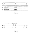
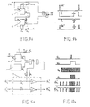
- Fig.1 shows the waves forms of the main driving pulses of the prior art solid state image pickup device (for example a interline transferring CCD (charge conpled device)), wherein ⁇ P is the string of the field charge integrating pulses, ch is the strring of the charge transfer controlling pulses, ⁇ V is the strring of the vertical shift clock pulses (only one phase shown here), t PH is the strring of the horizontal shift clock pulses (only one phase shown here).
- ⁇ P is the string of the field charge integrating pulses
- ch the strring of the charge transfer controlling pulses
- ⁇ V is the strring of the vertical shift clock pulses (only one phase shown here)
- t PH is the strring of the horizontal shift clock pulses (only one phase shown here).
- the light-produced charges are to be transferred from the photoelectrical converting units to the vertical shift registers, then the light-produced charges are shifted to the horizontal shift registers from line to line under ⁇ v driving, in turn the ligh-produced charges are read out to from the horizontal shift registers to an image signal processing means under t PH driving, at last the light-produced charges as video image signals are displaied on the screen of the videocorder.
- the present invention intents to change the driving pulse string cpp of the solid state image pickup device of prior art which has a charge integrating time of 20 ms per field into ⁇ ' P which has twin pulses for integrating charges per field, the first pulse is called the useless charge integrating pulse and the last pulse is called the useful charge integrating pulse.
- the present invention also intents to shorten the width of the useful charge integrating pulse in order to play a role of an electronic shutter.
- the speed of the "shutter” raises, as the width of the useful charge integrating pulse is shortened. When the width is shortened to 1ms, the speed of the "shutter” raises to 1/1000 second.
- the “shutter” differs from an additional shutter means.
- the "shutter” does not have a substantical additional shutter means, so its image pickup apparatus is at the exposure state from beginning to the end, while an additional shutter means is shut in normal times, and only at the moment when it is opened it is in the exposure state.
- the useful charge integrating time is 1ms
- the useless charge integrating time is 19ms. If the light-produced charges during the useless charge integrating time are cleared before the useful charges are integrated, the useful charges will be integrated on the clean "photographic plate" which is without the disturbance of the useless charges, thus clear images which is equivalent that of short exposure are obtained from the above, the present invention provides two methods for clearing useless charges (i.e. the "photographic plate” cleaning methods", the quickly pushing out method and the quickly discharging method. The difference between the two methods lies in, they have different ways of clearing the useless charges. In order to understand it easily, an interline transfer CCD will be described by way of an example.
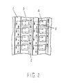
- Fig. 2 there are two channels for reading out the charges in the solid state image pickup device according to the present invention.
- the first reading out channel 1 both the useful integrating charges 4 (the image signal charges) in the photoelectrical converting units 3 and the useless integrating charge 5 in the photoelectrical converting units 3 are read out, while from the second reading out channel 2 only the useless integrating charges 5 are read out.
- the first reading out channle i.e. the conventional reading out channel of image charges for example an interline transfer CCD, comprises the vertical shift registers and the horizontal shift registers or an additional channel.
- the second reading out channel is the channel for the useless charges are quickly discharged, for example, with using OFCG configuration and applying a string of clearing pulses on it, it can make the useless charges quickly discharge from the discharging channel to the semiconductor substrate.
- the method for obtaining clear images of high speed moving objects which makes use of a solid state image pickup device to produce a solid state image pickup device having a high speed electronic shutter on itself to obtain clear images of high speed moving objects, is characterized by comprising the steps of:
- the second step reading the useless integrated charges and clearing out them very soon so as to clean the charge integrating regions and charge registering regions (which is called as the "photographic plate") for preparing the useful charges for being integrated on them where is no useless integrated charges disturb. Since useless integrated charges can be cleared out through two channels which are called as the first reading out channel and the second reading out channel.
- the first reading out channel comprises vertical shift registers and horizontal shift registers or an additional channel from the vertical shift registers to a substrate of the device.
- the method for clearing the useless integrated charges through the first channel uses two kinds of methods which are called as the quickly pushing out method or the quickly discharging method.
- the method for clearing the useless integrated charges through the second channel uses another discharging method.
- the quickly pushing out method is suitable to the current merchandised image pickup devices. It comprises the steps of:
- the quickly pushing out method has the features of easy putting in practice and a slight increase of cost, it still has the disadvantage of having a small range of adjustment of the "shutter speed", this is because that the lowest “shutter speed” is limited by the blanking time, and the fastest "shutter speed” is limited by the highest operating frequency of the vertical shift registers of the current merchadised image pickup devices.
- the current merchadised image pickup devices useally obtain such "shutter” speeds, about 1/1000, 1/2000 second.
- the improved configuration can obtain the "shutter” speed higher than that of the above.
- the quickly discharging method can only be used on the basis of changing the inner configuration of the image pickup devices, for example, an additional channel onto the substrate of the semiconductor can be added and arranged near the side of the vertical shift registers, so as to quickly discharge the useless integrated charges in the vertical shift registers of the first reading out channel to the substrate of the semiconductor under a clearing pulse string ⁇ L (Fig. 5) driving.
- Another discharging method is used to clear the useless integrated charges which is transfered to the second channel.
- This method is suitable to such image pickup devices which have the second reading out channel for discharging the charges to the substrate of the semiconductor, and the second reading out channel is arranged on the other side of the light-sensitive units, this side is not adjacent to the vertical shift registers, for instance, the overflow drain configuration havng OFCG (overflow control gate).
- clearing pulse string ⁇ L is applied onto the corresponding configuration. when ⁇ L is at high level, the useless integrated charges drain to the potential well and then to the substrate of the semiconductor of the device.
- OFD is an overflow drain
- OFCG is an overflow control gate
- PD is a phtotelectrical converting unit.
- V co a D.C. positive voltage
- the dotted lines representing the potential barrier between the photoelectrical converting unit PD and the vertical shift register V is one side of the three sides.
- the height of the potential barrier between OFD and PD can be controlled by adjusting the voltage V co of the OFCG. The higher is the V co , the lower is the height of the potential barrier, more charges will be drained.
- the "photographic plate" cleaning technology of the present invention is just developed on this base. The key point of the present invention is that the cleaning pulse string ⁇ L shown in Fig. 5 is applied onto the OFCG. The low level of ⁇ L is the D.C.
- the high level of ⁇ L is determined by the different configurations of the devices, but it should make the potential barrier between the OFD and the PD varish, for the drain of the useless integrated clarges all, so as to achieve the object of cleaning the "photographic plate".
- the width of the clearing pulse shown in fig. 5 can be used as both the dotted line and the real line.
- the principle of the clearing method of the present invention is that during the time of the useless charges being integrated, because the high level of ⁇ L is applied on the OFCG. the potential barrier between the OFD and the PD may vanish throughout, so that all the useless integrated charges areaned away, thus the object of cleaning the "photogratic plate is achieved.
- ⁇ P and q 5T in Fig. 5 still are one pulse per field, but T A and T b are the time of the useless charge integration and the time of the useful charge integration respectively, and the operating manner is still integration twice and reading out twice per field.
- This method for clearing the useless integrated charges through the second reading out channel compared with the above method which is through of the first reading out channel has an advantage that the slowest speed of its "shutter " is not limited by the time of the field blanking. Because the adjustment of the interval (T B ) between ⁇ L and ⁇ T shown in Fig. 5 is only related with the time of the useful integration and does not influence the reading out of the useful integrated charges through the first reading out channel at all. If the device can be drived at a clock with a frequency of kilo megahertz level, the interval T B can be wantonly adjusted within the range of 20ms to ns. If a timing means is added, the "shutter" speed can also have the range of that of the conventional shutter speed level such as 1/50, 1/125, 1/250 second and so on.
- the third step reading out the useful integrated charges which will be the image signal of the taken object through the first reading out channel, when using the quickly pushing out method, the useful integrated charges are read out from the vertical shift registers to the horizontal shift registers at the duration of the first clock frequency of which has the same frequency as o v , then the useful integrated charges are read out from the horizontal shift registers to a signal processing means under ⁇ H driving, at last as being the image signals they will be displayed on the screen of the videocorder.
- the apparatus of the present invention comprises a CCD image pickup device, a CCD driving pulse generator, a CCD driver and a signal processor.
- the image pickup apparatus of the present invention belongs to the kind of image pickup apparatus with low frame-frequency, short exposure, so when it is used for taking a high speed spinning body, the high speed spinning body can be sampled based on the field frequency.
- the frequency of the spinning body is equal to the integral times of the field frequency, because the sampled point of the image pickup apparatus each time is the same point of the same spinning body, it is the clear, relative still image of he spinning body reappeared on the videocorder.
- the frequency of the spinning body is higher than the integral times of the field frequency, it is the clear, slow, positively rotating image of the spinning body reappeared on the videocorder, it's rotating frequency is the least difference of the above two frequencies.
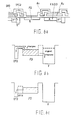
- Figs. 7a and 7b are the schematical principle block of the driving portion of the image pickup device of XC 37/38 and the wave forms of its driving pulses respectively.
- XC-37/38 pickup camera Since XC-37/38 pickup camera has an improvement in its configuration, so the pulses ⁇ P and ⁇ T are combined to form a new pulse string SG.
- SG When SG is at a high level, charges are integrated.
- SG When SG is lowered from a high level, the integrated charges are transferred to the vertical shift registers.
- the vertical shift pulse has two phases ⁇ v1 , and ⁇ v2 .
- the horizontal shift pulse is ⁇ H ( it is not shown in Fig. 7b).
- a CCD image pickup device is indicated in Fig. 7b with the reference number 6. Reference number 7 is referred to A CCD driver (inverted amplifier).
- a CCD driving pulse generator comprising a twin pulses generator for generating, which has twin pulses per field and a twin clock frequencies generator for generating which has two sets of clock pulses, within each set of clock pulses having a frequency, the first clock frequency being equal to the frequency of ⁇ V , the second clock being a high frequency having the dration T ( r ⁇ t 3 ), the beginning of the second set of clock pulses appears the particular time when the integration of the useless integrated charges just ends, is indicated by the reference number 8.
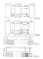
- Figs. 8a and 8b are the schematical principle block of the embodiment of the high speed image pickup apparatus of the present invention and the wave forms of its driving pulses respectively.
- the twin pulses generator is indicated by the reference number 9.
- Reference number 10 and 11 are the twin clock generators.
- the quickly pushing out method is employed in the said embodiment, through which all useless integrated charges are cleared through the first reading out channel.
- the charge integrating pulse string SG" having two pulses per field and the clock pulse strings and having two pulses per field are all shown in Fig. 8b.
- Figs 9a,9b and Figs. 10a, 10b are the specific circuits and the wave forms for generating the above twin pulses and twin clocks, respectively.
- the twin pulses generator also comprises a timing means for adjusting the electronic shutter speed of the device on itself, and the twin clock frequencies generator comprises a high frequency generator for generating said high frequency pulses of the vertical shift clock pulse string for cleaning the "photographic plate".
- Figs. 9a and 9b shown, when the field integrating pulse SG' is raised from a low level to a high level (indicated by TR+), the monostable flip-flop 12 is triggered and a negative pulse with a width of ⁇ 1 can be obtained at the output terminal Q 1 .
- ⁇ 1 is determined by the multiplication of R 1 and C 1 .
- the width 71 of the negative pulse can be changed, as R 1 being adjusted, that is, the time of the useless charge integration is changed.
- the time of the field scanning is given, the wider is the 71 , the shorter is the opening time of the "shutter".
- the negative pulse from the output terminal Q 1 then triggers the monostable flip-flop 13 and the negative pulse with the width of T2 which is determined by the multiplication of R 2 and C 2 is obtaned at the output terminal Q 2 .
- the AND NOT gate C Only when Q3 is at a high level, the AND NOT gate C provides high frequency pulse output, the high frequency pulse outputs with the duration time 73 provided by the AND NOT gates C and D through the resistances R 4 and R 5 respectively and the two- phase vertical shift pulses and through resistance R 6 and R 7 are added at the input terminal the amplifier E and F. Therefore and are obtained at the output terminals of E and F respectively.
- the duration time of the high frequency clock can not exceed the time of the useful integration (that is the opening time of the electronic shutter).
- FIG. 8b the interval T A between the first pulse of SG" relative to the pulse of SG (Fig. 7b) and the second pulse of SG" is the useless integrating time.
- the useless integrated charges are to be transferred to the vertical shift registers of the first reading out channel.
- the useful integrated charges begin to integrate on the cleaned" photographic plate" which was just cleaned.
- the high frequency clock pulses of and are applied to the vertical shift registers.
Abstract
This method is a direct development method for achieving a solid state image pickup device with a high speed electronic shutter on itself. A field integrating time is divided into a useless integrating time and a useful integrating time. The shorter one is the useful integrating time, the faster one is the electronic shutter speed. The useless integrated charges are cleared by the 'photographic plate" clearing method. This image pickup camera apparatus is a high speed image pickup camera apparatus having low or slight high frame frequency, short exposure. A clear, relatively still or very slowly spinning images can be obtained by adjusting the field frequency of the high speed pickup camera apparatus.
Description
- The present invention generally relates to a method and apparatus for obtaining clear images of high speed moving objects, in particular, relates to such a method and apparatus whereby an electronic shutter function of a solid state image pickup device on itself is developed.
- As far as an ordinary pickup camera goes, because it's image pickup device has inertia and low speed shutter, it is absolutely impossible to obtain clear images of high speed moving objects such as a quickly running car or a motorcar, a rotating rotor of a generator or of a motor and a spinning spindle of a spinning machine. A solid state image pickup device of an ordinary solid state pickup camera is one of the devices having the least inertia so far. when it operates at PAL television system, the charge integrating time is 20 ms per field corresponding to a shutter having an exposure time of 1/50 second. Thus, an image of a high speed moving object on the image pickup device has brought forth obvious movements i.e. repeated exposures within 20ms, therefore the ordinary solid state pickup camera is still impossible to obtain clear images of high speed moving objects. An ordinary high speed solid state pickup camera comprises an ordinary solid state pickup camera and an additional mechanical shutter or electronic shutter. Disadvantages of mechanical shutters are its poor opening property, poor stability, poor reliablity and limitary life time. Disadvantages of electronic shutters made of PLZT (Pb-Based Lanthanum-Doped Zirconate Titanates) used in the apparatus discribed in the article entitled "Electronic shutter CCD Pickup Camera" in "Mapping Imfomation"Japan Vol. 16, No. 6, P87 are that its control circuit is huge and complicated, because of its dielectric constant is up to 4000 at room temperature, it results in a quite high electric field required for controlling the electronic shutter, for example, a PLZT piece with 1mm in thickness requires an electric field of 450v/mm, so it is expensive, and that the PLZT light-sensitive devices have poor transmissivity, loss of more light and limitary life time. Particularly it is costly to shorten its opening time. This is the fatal weakness of the PLZT electronic shutter device.

- The method for reading out image charges from field to field described in No. 456766 U.S. Patent entitled "Method for driving solid state image pickup device" is that charges in a group of photoelectric conversion. elements of odd rows are to be read out in the first field of a frame and to be cleared out in the second field of the frame and charges in the group of photo-electric conversion elements of even rows are to be read out in the second field of the frame and to be cleared out in the first field of another frame. Although the said method keeps the advantage of the interlaced scanning and develops an electronic shutter of the image pickup device on itself, it only raises the corresponding shutter speed from 1/30 second to 1/60 second. It is evidant that the shutter speed is not enough to eliminate the image blur caused by repeated exposures of a high speed moving object.
- The main object of the present invention is to overcome the disadvantages of solid state image pickup cameras of the prior art and to provide a method for developing an electronic shutter function of a solid state image pickup device on itself and for making its "shutter" speed up to 1/1000, 1/2000 second or more higher, and an apparatus for obtaining clear images of high speed moving objects without an additonal shutter, so that the disadvantages of adding an additional shutter vanish from themselves and the cost reduces greatly.
- Another object of the present invention is to provide a new type of high speed solid state pickup camera apparatus having its "shutter" speed easy to adjust, which can be adjusted not only continueously, but also by the conventional grades such as 1/50,..., 1/1000, 1/2000 second or more, which is both used as an ordinary pickup camera and as a high speed pickup camera.
- Still another object of the present invention is to make the "electronic shutters" of the several pickup cameras apparatus of the present invention be controlled respectively to take the same object so as to increase image numbers per second on a screen of a videocorder.
- Still another object of the present invention is to provide a method for obtaining clear, relative still or slowrotating images of high speed spinning bodies such as machine tools, spinning machines, generators, motors and so on.
- The above objects and other objects, features and advantages of the present invention will be further evident from the detail description referring to the drawings as below:
- Fig. 1 shows the waves forms of the main driving pulses of a solid state image pickup device in prior art;
- Fig. 2 shows schematially the useful charges and useless charges in the solid state image pickup device reading out through the first channel and the second channel respectively;
- Fig. 3 shows the time relationship between the twice integrations and the twice readouts per field according to the present invention;
- Fig. 4 shows the waves forms of the pulses of the clearing method for quickly pushing out the useless integrating charges;
- Fig. 5 shows the waves forms of the pulses of the clearing method for discharging the useless integrating charges through the second channel;
- Fig. 6a shows a cross section of photoelectrical converting units of a interline transferring pickup camera, Fig. 6b shows a surface potential distribution while the image pickup device uses the overflow drain, Fig. 6c shows a surface potential distribution while the image pickup device uses to clear the 'photographic plate";
- Fig. 7a and 7b are the schematical block and the waves forms of the driving pulses of XC 37/38 pickup carmera produced by the Sony corporation in Japan respectively;
- Fig. 8a and 8b are the schematical block and the waves forms of the driving pulses of the high speed image pickup apparatus of the embodiment of the present invention respectively.
- Fig. 9a and 9b are the circuit of the twin pulses generator and the wave forms of the pulses respectively.
- Fig. 10a and 10b are the circuit of the twin clock pulses generator and the wave forms of the pulses respectively.
- Now referring to Fig.1. Fig.1 shows the waves forms of the main driving pulses of the prior art solid state image pickup device (for example a interline transferring CCD (charge conpled device)), wherein φP is the string of the field charge integrating pulses, ch is the strring of the charge transfer controlling pulses, φV is the strring of the vertical shift clock pulses (only one phase shown here), tPH is the strring of the horizontal shift clock pulses (only one phase shown here). when φP is at high level and φT is at low level, the photoelectrical converting units integrate light-produced charges. When φP is at low level and φT is at high level, the light-produced charges are to be transferred from the photoelectrical converting units to the vertical shift registers, then the light-produced charges are shifted to the horizontal shift registers from line to line under ϕv driving, in turn the ligh-produced charges are read out to from the horizontal shift registers to an image signal processing means under tPH driving, at last the light-produced charges as video image signals are displaied on the screen of the videocorder.
- The present invention intents to change the driving pulse string cpp of the solid state image pickup device of prior art which has a charge integrating time of 20 ms per field into φ'P which has twin pulses for integrating charges per field, the first pulse is called the useless charge integrating pulse and the last pulse is called the useful charge integrating pulse. The present invention also intents to shorten the width of the useful charge integrating pulse in order to play a role of an electronic shutter. The speed of the "shutter" raises, as the width of the useful charge integrating pulse is shortened. When the width is shortened to 1ms, the speed of the "shutter" raises to 1/1000 second. The "shutter" differs from an additional shutter means. Because the "shutter" does not have a substantical additional shutter means, so its image pickup apparatus is at the exposure state from beginning to the end, while an additional shutter means is shut in normal times, and only at the moment when it is opened it is in the exposure state. When the useful charge integrating time is 1ms, the useless charge integrating time is 19ms. If the light-produced charges during the useless charge integrating time are cleared before the useful charges are integrated, the useful charges will be integrated on the clean "photographic plate" which is without the disturbance of the useless charges, thus clear images which is equivalent that of short exposure are obtained from the above, the present invention provides two methods for clearing useless charges (i.e. the "photographic plate" cleaning methods", the quickly pushing out method and the quickly discharging method. The difference between the two methods lies in, they have different ways of clearing the useless charges. In order to understand it easily, an interline transfer CCD will be described by way of an example.
- As Fig. 2 shown, there are two channels for reading out the charges in the solid state image pickup device according to the present invention. From the first reading out
channel 1, both the useful integrating charges 4 (the image signal charges) in the photoelectrical convertingunits 3 and the useless integratingcharge 5 in the photoelectrical convertingunits 3 are read out, while from the second reading outchannel 2 only the useless integratingcharges 5 are read out. The first reading out channle, i.e. the conventional reading out channel of image charges for example an interline transfer CCD, comprises the vertical shift registers and the horizontal shift registers or an additional channel. The second reading out channel is the channel for the useless charges are quickly discharged, for example, with using OFCG configuration and applying a string of clearing pulses on it, it can make the useless charges quickly discharge from the discharging channel to the semiconductor substrate. - The method for obtaining clear images of high speed moving objects, which makes use of a solid state image pickup device to produce a solid state image pickup device having a high speed electronic shutter on itself to obtain clear images of high speed moving objects, is characterized by comprising the steps of:
- The first step, generating a field charge integrating pulse string φ'P and a charge transfer controlling pulse string φ'T. As shown in Fig. 3, ϕ p and φ'T have twin pulses per field. The first pulse is the useless charge integrating pulse having the duration t1. The second pulse is the useful charge integrating pulse having the duration t3. Because ϕ p and φ'T add one more pulse per field, than φP and φT, the reading out manner of the integrating charges changes from once per field of the prior art into twice per field, particular, during ti useless charges are integrated in photoelectrical units; while during t2 the useless charges are read out (or cleared out), which is to clean the "photographic plate "and to empty it and to prepare the useful charges for being integrated on it, as a result no useless charges disturb within the period of useful charges being integrated; during t3 useful charges are integrated; during t4 the useful integrated charges representing the image signals of the taken object are read out to the vertical shift registers of the first reading out channel. The shorter is the time of the said useful charge integration, the faster is the said "shutter" speed.
- The second step, reading the useless integrated charges and clearing out them very soon so as to clean the charge integrating regions and charge registering regions (which is called as the "photographic plate") for preparing the useful charges for being integrated on them where is no useless integrated charges disturb. Since useless integrated charges can be cleared out through two channels which are called as the first reading out channel and the second reading out channel. The first reading out channel comprises vertical shift registers and horizontal shift registers or an additional channel from the vertical shift registers to a substrate of the device. The method for clearing the useless integrated charges through the first channel uses two kinds of methods which are called as the quickly pushing out method or the quickly discharging method. The method for clearing the useless integrated charges through the second channel uses another discharging method.
- The quickly pushing out method is suitable to the current merchandised image pickup devices. it comprises the steps of:
- generating the vertical shift clock pulse string φ'V, as shownin Fig. 4 which comprises two sets of clock pulses, within each set of clock pulses having a frequecy, the first clock frequency is equal to the clock frequency of φV (Fig. 1) and the - second clock frequency is a high frequency having the duration T ( 7 < ts ), the beginning of which appears at particular times when the integration of the useless integrated charges just ends.
- Pushing out the useless integrated charges in the vertical shift registers to the horizontal shift registers under the control of the second clock of φ'V during so that the vertical shift registers can be cleared. Then reading out the useless integrated charges in the horizontal shift registers to a signal processing means under φH driving. It is understandable that during the time when quickly pushing out the useless integrated charges, the horizontal shift registers are faced the stroke of the impact wave-gushing-like of the useless integrated charges. Because the duration T corresponds to the time of several lines, the useless integrated charges will appear on a screen as several bright lines.
- If the time of the useful charge integration (i.e. the time of the "shutter" openning) is longer than the time of the field blanking, the several bright lines will be blanked. If the time of- the useful charge integration is shorter than the time of the field blanking. the several bright lines will be appeared on the image. Thus it can be seen that although the quickly pushing out method has the features of easy putting in practice and a slight increase of cost, it still has the disadvantage of having a small range of adjustment of the "shutter speed", this is because that the lowest "shutter speed" is limited by the blanking time, and the fastest "shutter speed" is limited by the highest operating frequency of the vertical shift registers of the current merchadised image pickup devices. The current merchadised image pickup devices useally obtain such "shutter" speeds, about 1/1000, 1/2000 second. The improved configuration can obtain the "shutter" speed higher than that of the above.
- The quickly discharging method can only be used on the basis of changing the inner configuration of the image pickup devices, for example, an additional channel onto the substrate of the semiconductor can be added and arranged near the side of the vertical shift registers, so as to quickly discharge the useless integrated charges in the vertical shift registers of the first reading out channel to the substrate of the semiconductor under a clearing pulse string φL(Fig. 5) driving.
- Another discharging method is used to clear the useless integrated charges which is transfered to the second channel. This method is suitable to such image pickup devices which have the second reading out channel for discharging the charges to the substrate of the semiconductor, and the second reading out channel is arranged on the other side of the light-sensitive units, this side is not adjacent to the vertical shift registers, for instance, the overflow drain configuration havng OFCG (overflow control gate). As shown in Fig. 5, clearing pulse string φL is applied onto the corresponding configuration. when φL is at high level, the useless integrated charges drain to the potential well and then to the substrate of the semiconductor of the device.
- Now the process for clearing the useless integrated charges will be described by way of example of an integrline transfer CCD with OFCG as shown in Fig. 6a. In Fig. 6a OFD is an overflow drain, OFCG is an overflow control gate, PD is a phtotelectrical converting unit. When the device is used as the overflow drain, a D.C. positive voltage Vco is applied to the OFCG so that the height of the potential barrier between the controlled OFD and PD is slightly lower than that of the other three sides of the PD potential well as shown in Fig. 6b, the dotted lines representing the potential barrier between the photoelectrical converting unit PD and the vertical shift register V is one side of the three sides. When strong light shines on it, excessive charges will be drained to the OFD through the slight lower potential barrier, so as to restrain the diffusion phenomenon. The height of the potential barrier between OFD and PD can be controlled by adjusting the voltage Vco of the OFCG. The higher is the Vco, the lower is the height of the potential barrier, more charges will be drained. The "photographic plate" cleaning technology of the present invention is just developed on this base. The key point of the present invention is that the cleaning pulse string φL shown in Fig. 5 is applied onto the OFCG. The low level of φL is the D.C. voltage Vco , the high level of φL is determined by the different configurations of the devices, but it should make the potential barrier between the OFD and the PD varish, for the drain of the useless integrated clarges all, so as to achieve the object of cleaning the "photographic plate". The width of the clearing pulse shown in fig. 5 can be used as both the dotted line and the real line. The principle of the clearing method of the present invention is that during the time of the useless charges being integrated, because the high level of φL is applied on the OFCG. the potential barrier between the OFD and the PD may vanish throughout, so that all the useless integrated charges are darined away, thus the object of cleaning the "photogratic plate is achieved. At the moment when the useless charge integration ends, the level of φL is changed from high to low OFCD is to restore to Vco the useful charge integration begins. At this moment the surface potential distribution of the device is as that shown in Fig. 6b, the potential barrier of a certain height are formed again between the OFD and the PD, from which the normal integration and the transfer of the useful integrated charges on the clean "photographic plate" are guaranteed, therefore, clear images will be obtained.
- It should be noted that φP and q5T in Fig. 5 still are one pulse per field, but TA and Tb are the time of the useless charge integration and the time of the useful charge integration respectively, and the operating manner is still integration twice and reading out twice per field.
- Of course, other configurations can also be used for clearing the useless integrated charges. This method for clearing the useless integrated charges through the second reading out channel compared with the above method which is through of the first reading out channel has an advantage that the slowest speed of its "shutter " is not limited by the time of the field blanking. Because the adjustment of the interval (TB) between φL and φT shown in Fig. 5 is only related with the time of the useful integration and does not influence the reading out of the useful integrated charges through the first reading out channel at all. If the device can be drived at a clock with a frequency of kilo megahertz level, the interval TB can be wantonly adjusted within the range of 20ms to ns. If a timing means is added, the "shutter" speed can also have the range of that of the conventional shutter speed level such as 1/50, 1/125, 1/250 second and so on.
- The third step, reading out the useful integrated charges which will be the image signal of the taken object through the first reading out channel, when using the quickly pushing out method, the useful integrated charges are read out from the vertical shift registers to the horizontal shift registers at the duration of the first clock frequency of

- Because the image pickup apparatus developed by the method of the present invention is a kind of high speed image pickup camera with low frame frequency, low cost, having electronic shutter on itself, it can be connected with an ordinary videocorder, therefore the cost necessary to form a complete set is low and the image signals of high speed moving objects can easily be processed by means of an ordinary microprocessor. The apparatus of the present invention comprises a CCD image pickup device, a CCD driving pulse generator, a CCD driver and a signal processor. When several above image pickup apparatus are connected with a videocorder and take the same object, their electronic shutters are respectively controlled in their given order by a pulse distributor so that the effect of increasing image numbers per second can be obtained.
- Because the image pickup apparatus of the present invention belongs to the kind of image pickup apparatus with low frame-frequency, short exposure, so when it is used for taking a high speed spinning body, the high speed spinning body can be sampled based on the field frequency. When the frequency of the spinning body is equal to the integral times of the field frequency, because the sampled point of the image pickup apparatus each time is the same point of the same spinning body, it is the clear, relative still image of he spinning body reappeared on the videocorder. When the frequency of the spinning body is higher than the integral times of the field frequency, it is the clear, slow, positively rotating image of the spinning body reappeared on the videocorder, it's rotating frequency is the least difference of the above two frequencies. Otherwise, it is a clear, slow, negatively rotating image of the spinning body reappeared on the videocorder. Further, a clear relative still, image of the high speed spinning body can be obtained by adjusting the clock frequencies of the image pickup camera apparatus of the present invention. Therefore, it is very convenient to do the monitoring, repairing, and turning of a high speed spinning body by using the image pickup camera apparatus of the present invention, particularly, it is suitable to monitor the quickly running car along the high speed road, because this case does not require handrends of even thousands of images per second.
- An embodiment using the quickly pushing out method with the XC 37/38 black and white CCD image pickup camera produced by the Sony corporation in Japan will now be described below.
- Figs. 7a and 7b are the schematical principle block of the driving portion of the image pickup device of XC 37/38 and the wave forms of its driving pulses respectively.
- Since XC-37/38 pickup camera has an improvement in its configuration, so the pulses φP and φT are combined to form a new pulse string SG. When SG is at a high level, charges are integrated. When SG is lowered from a high level, the integrated charges are transferred to the vertical shift registers. The vertical shift pulse has two phases φv1, and φv2. The horizontal shift pulse is φH ( it is not shown in Fig. 7b). A CCD image pickup device is indicated in Fig. 7b with the
reference number 6.Reference number 7 is referred to A CCD driver (inverted amplifier). A CCD driving pulse generator comprising a twin pulses generator for generating,

reference number 8. - Figs. 8a and 8b are the schematical principle block of the embodiment of the high speed image pickup apparatus of the present invention and the wave forms of its driving pulses respectively. In Fig. 8a, the twin pulses generator is indicated by the reference number 9.
Reference number 10 and 11 are the twin clock generators. The quickly pushing out method is employed in the said embodiment, through which all useless integrated charges are cleared through the first reading out channel. The charge integrating pulse string SG" having two pulses per field and the clock pulse strings

- Figs 9a,9b and Figs. 10a, 10b are the specific circuits and the wave forms for generating the above twin pulses and twin clocks, respectively.
- The twin pulses generator also comprises a timing means for adjusting the electronic shutter speed of the device on itself, and the twin clock frequencies generator comprises a high frequency generator for generating said high frequency pulses of the vertical shift clock pulse string

- As Figs. 9a and 9b shown, when the field integrating pulse SG' is raised from a low level to a high level (indicated by TR+), the monostable flip-
flop 12 is triggered and a negative pulse with a width of τ1 can be obtained at the output terminalQ 1 . τ1 is determined by the multiplication of R1 and C1. The width 71 of the negative pulse can be changed, as R1 being adjusted, that is, the time of the useless charge integration is changed. When the time of the field scanning is given, the wider is the 71, the shorter is the opening time of the "shutter". The negative pulse from the output terminalQ 1, then triggers the monostable flip-flop 13 and the negative pulse with the width of T2 which is determined by the multiplication of R2 and C2 is obtaned at the output terminal Q 2 . Let r2 be equal the width of SG' by adjusting R2. After the pulse with the width of r2 and SG' which is inverted by the AND NOT gate A are added at the AND NOT gate B, the SG" is obtained which has twin pulses per field. - Referring to Figs. 10a and 10b, when the mon- stable flip-flop 14 is triggered by the positive pulse from the output terminal Q2 of the monostable flip-
flop 13, the positive pulse with the width of T3 is obtained at the output terminal Q3. This positive pulse with its width T3 is applied to one of the input terminal of the AND NOT gate C. And the output terminal of the high frequency pulse generator 15 having continuous, oscillation is connected to the other input terminal of the AND NOT gate C. Only when Q3 is at a high level, the AND NOT gate C provides high frequency pulse output, the high frequency pulse outputs with the duration time 73 provided by the AND NOT gates C and D through the resistances R4 and R5 respectively and the two-


- A image pickup camera produced by Sony Corporation has been modified as a high speed image pickup apparatus. Now the process of its operation is described below. Referring to Fig. 8b, the interval TA between the first pulse of SG" relative to the pulse of SG (Fig. 7b) and the second pulse of SG" is the useless integrating time. Upon ending the useless integration (that is, upon ending T A), the useless integrated charges are to be transferred to the vertical shift registers of the first reading out channel. Then upon arising the arise edge of the second pulse of SG", the useful integrated charges begin to integrate on the cleaned" photographic plate" which was just cleaned. At the same time, the high frequency clock pulses of


- Although the present invention has been described herein, with regard to an examplary embodiment, it is understood that other configurations or arrangements may be developed which nevertheless do not depart from the spirit and scope of the present invention.
Claims (8)
1. A method for obtaining clear images of high speed moving objects, which develops a solid state image pickup device a a solid state image pickup device with a high speed electronic shutter on itself to clear images of high speed moving objects, the said method is characterized by comprising the steps of:
The first step, generating a field charge integrating pulse string ( 
) and a charge transfer controlling pulse string ( 
) (they (4) and ( 
) have twin pulses per field) to integrate charges in photoelectrical units twice per field under the said field integrating pulse string ( 
) driving, and to read out the said integrated charges to vertical shift registers twice each field under the said charge transfer controlling pulse string ( 
) driving, the said integrated charges comprising useful integrated charges and useless integrated charges, the shorter being the time of the said useful charge integration, the faster being the said " shutter speed;
the second step, reading out the said useless integrated charges and clearing out them very soon so as to clean the charge integrating regions and charge registering regions (which is as "photographic plate"), for preparing the said useful charges for being integrated on said "photographic plate" where no said useless integrated charges disturb;
clearing said useless integrated charges through two reading out channels, the first reading out channel comprises vertical shift registers and horizontal shift registers or an additional channel from said vertical shift registers leading to a substrate of said solid state image pickup device, and the second reading out channel is from the photoelectrical converting units to the substrate of the said device; clearing the said useless integrated charges through the said first channel using the quickly pushing out method or the quickly discharging method, clearing the said useless integrated charges through the said second channel using another discharging method;
the third step, reading out the said useful integrated charges which will be image signals through the said first reading out channel.
2. The method according to claim 1, wherein the said quickly pushing out method comprising the steps of:
generating a vertical shift clock pulse string ( 
) which comprises two sets of clock pulses within each set of clock pulses having a frequency, a frist clock frequency being equal to the clock frequency of the conventtional vertical shift clock pulse string (φv), a second clock frequency being a high frequency having the duration time (1) (7 being less than the duration time (t3) of the seocnd pulse of said field charge integrating pulse string ( 
)), the beginning of said second set of clock pulses appearing at the particular time when the said integration of the useless integrated charges just ending;
pushing out the said useless integrated charges in the said vertical shift registers to the said horizontal shift registers under the said second clock of said vertical shift clock pulse string ( 
) during the said duration time (r);
reading out the said useless integrated charges in the said horizontal shift registers to a signal processing means under a conventinal horizontal shift clock pulse string (φH) driving.
3. The method according to claim 1, wherein said quickly discharging method compring the steps of:
discharging the said useless intetrated charges in said vertical shift registers through said additional channel to the substrate of said device under a clearing pulse string (φL) driving.
4. The method according to claim 1,wherein the other said discharging method comprising the steps of:
draining the said useless integrated charges in said photoelectric converting units to said second reading out channel under said clearing pulse string (φL) driving;
discharging the said useless integrated charges through the said second reading out channel to the substrate of said device.
5. The method according to claim 1, wherein the step of reading out the said useful integrated charges in the said vertical shift registers of said first reading out channel to said horizontal shift registers of said first reading out channel is under the said first clock of said vertical shift clock pulse string ( 
) driving during the duration time of said first clock of said vertical shift clock pulse string (ϕ ); );
the step of reading out the said useful integrated charges which will be image signals in said horizontal shift registers to said signal processing means is under said conventional horzontal shift clock pulse string (φH) driving.
6. An apparatus for obtaining clear images of high speed moving objects, comprising:
said apparatus being characterized in that said CCD driving pulse generator comprising a twin pulses generator for generating said field charge integrating pulse string ( 
) which has twin pulses per field, which are a useless charge integrating pulse and a useful charge integrating pulse, and a twin clock frequencies generator for generating said vertical shift clock pulse string (φ'v) which comprises two sets of clock pulses, within each set of clock pulses having a frequency, a first clock frequency being equal to the frequency of the said conventional vertical shift clock pulse string (φv), a second clock frequency being a high frequency having said druation time (T) (T being less than said druation time (t3) of the second pulse of said field charge integrating pulse string ( 
), the beginning of the said second set of clock pulses appearing at the particular time when the said integration of said useless integrated charges just ends.
A CCD image pickup device,
A CCD driving pulse generator,
A CCD driver, and
A signal processor,
said apparatus being characterized in that said CCD driving pulse generator comprising a twin pulses generator for generating said field charge integrating pulse string (
7. An apparatus according to claim 6, wherein said twin pulses generator also comprising a timing means for adjusting said electronic shutter speed of said device on itself; said twin clock frequencies generator comprising a high frequency generator for generating said high frequency pulses of said vertical shift clock pulse string ( 
) for cleaning said photographic plate".
8. A method for obtaining clear, relatively still or very slowly spinning images of high speed spinning bodies, said method being characterized by comprising the steps of:
sampling said high spinning speed of said high speed spinning body by said field frequency;
adjusting said field frequency of of said image pickup camera apparatus when the spinning frequency of said spinning body is equal to the integral times of said field frequency, a clear, relatively still image of said spinning body can be obtained; when said spinning frequency of said spinning body is higher than integral times of said field frequency, a clear, very slow, positively rotating image of said spinning body can be obtained; when said spinning frequency of said spinning body is lower than the integral times of said field frequency, a clear very slow, negatively rotating image of said spinning body can be obtained.
Applications Claiming Priority (4)
| Application Number | Priority Date | Filing Date | Title |
|---|---|---|---|
| CN86205900 | 1986-08-11 | ||
| CN 86205900 CN86205900U (en) | 1986-08-11 | 1986-08-11 | Ccd high-speed pick-up camera with electro-shutter |
| CN 86107106 CN86107106A (en) | 1986-10-18 | 1986-10-18 | The high speed solid state pick-up camera of self equipped with electronic shutter |
| CN86107106 | 1986-10-18 |
Publications (1)
| Publication Number | Publication Date |
|---|---|
| EP0256464A2 true EP0256464A2 (en) | 1988-02-24 |
Family
ID=25742256
Family Applications (1)
| Application Number | Title | Priority Date | Filing Date |
|---|---|---|---|
| EP87111520A Withdrawn EP0256464A2 (en) | 1986-08-11 | 1987-08-08 | Method and apparatus for obtaining clear images of high speed moving objects |
Country Status (3)
| Country | Link |
|---|---|
| US (1) | US4851915A (en) |
| EP (1) | EP0256464A2 (en) |
| JP (1) | JPS63266976A (en) |
Cited By (3)
| Publication number | Priority date | Publication date | Assignee | Title |
|---|---|---|---|---|
| EP0372456A2 (en) * | 1988-12-07 | 1990-06-13 | Nec Corporation | CCD image sensor with vertical overflow drain |
| FR2640836A1 (en) * | 1988-12-15 | 1990-06-22 | Asahi Chemical Ind | APPARATUS FOR CONTROLLING AN IMAGE RECEIVING DEVICE |
| US5282041A (en) * | 1988-12-15 | 1994-01-25 | Asahi Kogaku Kogyo Kabushiki Kaisha | Apparatus for driving image pick-up device |
Families Citing this family (10)
| Publication number | Priority date | Publication date | Assignee | Title |
|---|---|---|---|---|
| EP0387817A3 (en) * | 1989-03-16 | 1991-12-11 | Konica Corporation | Electronic still camera |
| US4975777A (en) * | 1989-06-15 | 1990-12-04 | Eastman Kodak Company | Charge-coupled imager with dual gate anti-blooming structure |
| JP2818214B2 (en) * | 1989-08-31 | 1998-10-30 | 株式会社東芝 | Solid-state imaging device |
| US4974043A (en) * | 1989-10-12 | 1990-11-27 | Eastman Kodak Company | Solid-state image sensor |
| JPH04170175A (en) * | 1990-11-02 | 1992-06-17 | Canon Inc | Driver for solid-state image pickup element |
| AU1995092A (en) * | 1991-05-10 | 1992-12-30 | Q-Dot. Inc. | High-speed peristaltic ccd imager with gaas fet output |
| US6259478B1 (en) * | 1994-04-01 | 2001-07-10 | Toshikazu Hori | Full frame electronic shutter camera |
| US5559553A (en) * | 1994-10-28 | 1996-09-24 | Eastman Kodak Company | Clock control circuit with independent timing adjustments for image sensing devices |
| JPH0997894A (en) * | 1995-09-29 | 1997-04-08 | Sanyo Electric Co Ltd | Solid-state image pickup device and its driving method |
| CA2378066A1 (en) | 1999-08-17 | 2001-02-22 | Applied Vision Systems, Inc. | Improved dynamic range video camera, recording system, and recording method |
Family Cites Families (6)
| Publication number | Priority date | Publication date | Assignee | Title |
|---|---|---|---|---|
| US3931463A (en) * | 1974-07-23 | 1976-01-06 | Rca Corporation | Scene brightness compensation system with charge transfer imager |
| US4564766A (en) * | 1982-04-20 | 1986-01-14 | Matsushita Electric Industrial Co., Ltd. | Method for driving solid state image pickup device |
| US4577115A (en) * | 1982-11-08 | 1986-03-18 | Rca Corporation | Apparatus for sensing transient phenomena in radiant energy images |
| US4573078A (en) * | 1982-11-08 | 1986-02-25 | Rca Corporation | Method for operating a CCD imager of the field transfer type |
| JPH07114472B2 (en) * | 1984-11-19 | 1995-12-06 | 株式会社ニコン | Driving method for solid-state imaging device |
| US4564666A (en) * | 1985-03-11 | 1986-01-14 | Desoto, Inc. | Urethane acrylates based on polyepichlorohydrin polyether diols and optical fiber coatings based thereon |
-
1987
- 1987-08-07 US US07/082,628 patent/US4851915A/en not_active Expired - Fee Related
- 1987-08-08 EP EP87111520A patent/EP0256464A2/en not_active Withdrawn
- 1987-08-11 JP JP62199254A patent/JPS63266976A/en active Pending
Cited By (8)
| Publication number | Priority date | Publication date | Assignee | Title |
|---|---|---|---|---|
| EP0372456A2 (en) * | 1988-12-07 | 1990-06-13 | Nec Corporation | CCD image sensor with vertical overflow drain |
| EP0372456A3 (en) * | 1988-12-07 | 1991-12-27 | Nec Corporation | Ccd image sensor with vertical overflow drain |
| FR2640836A1 (en) * | 1988-12-15 | 1990-06-22 | Asahi Chemical Ind | APPARATUS FOR CONTROLLING AN IMAGE RECEIVING DEVICE |
| FR2645695A1 (en) * | 1988-12-15 | 1990-10-12 | Asahi Optical Co Ltd | APPARATUS FOR CONTROLLING AN IMAGE RECOVERY DEVICE WITH TRANSFER AND CHARGE SCAN |
| FR2645696A1 (en) * | 1988-12-15 | 1990-10-12 | Asahi Optical Co Ltd | APPARATUS FOR CONTROLLING A LOAD TRANSFER IMAGE SENSING DEVICE WITH REGISTRATION TIME REGULATION |
| US5282041A (en) * | 1988-12-15 | 1994-01-25 | Asahi Kogaku Kogyo Kabushiki Kaisha | Apparatus for driving image pick-up device |
| FR2700907A1 (en) * | 1988-12-15 | 1994-07-29 | Asahi Optical Co Ltd | Apparatus for controlling a charge transfer imaging means |
| US5416517A (en) * | 1988-12-15 | 1995-05-16 | Tani; Nobuhiro | Apparatus for driving image pick-up device including smear prevention |
Also Published As
| Publication number | Publication date |
|---|---|
| US4851915A (en) | 1989-07-25 |
| JPS63266976A (en) | 1988-11-04 |
Similar Documents
| Publication | Publication Date | Title |
|---|---|---|
| US4884142A (en) | Electronic camera having solid state image sensor with improved noise signal draining | |
| EP0256464A2 (en) | Method and apparatus for obtaining clear images of high speed moving objects | |
| EP0573235B1 (en) | Solid-state image pick-up apparatus with integration time control | |
| US20010043276A1 (en) | Imaging device including thinned read out mode and all pixel read out mode | |
| EP0195270B1 (en) | Video camera apparatus | |
| DE3405808A1 (en) | IMAGE RECORDING DEVICE | |
| US5339162A (en) | Driving apparatus of image pick-up device for preventing leakage of accumulated electrical charges | |
| US4338634A (en) | Frame-rate converting film scanner with two-dimensional solid state image sensing array | |
| US5047875A (en) | Recording system which can record signals from two fields for the composition of one picture | |
| US20030090582A1 (en) | Imaging apparatus and control device therefor technical field | |
| JPH022793A (en) | Two-dimensional ccd image pickup element driving method | |
| US4564766A (en) | Method for driving solid state image pickup device | |
| US4866528A (en) | Image pickup apparatus providing lessened flicker in electronic still cameras and the like | |
| JPH01165271A (en) | Solid-state image pickup device | |
| JPS5930378A (en) | Image pickup device | |
| JPH0374554B2 (en) | ||
| JPS58212167A (en) | Interline transfer charge coupled element | |
| JP2000134540A (en) | Solid-state image pickup device and its driving method | |
| US5212599A (en) | Electronic camera for synchronous recording of still pictures on rotating record medium | |
| US5317455A (en) | Recording system which can record signals from two fields for the composition of one picture | |
| JPS5913474A (en) | Image pick-up device | |
| JPS59115681A (en) | Image pickup and recording device | |
| JPH0320956B2 (en) | ||
| JP2630492B2 (en) | Solid-state imaging device | |
| JPH0646341A (en) | Solid-state image pickup device |
Legal Events
| Date | Code | Title | Description |
|---|---|---|---|
| PUAI | Public reference made under article 153(3) epc to a published international application that has entered the european phase |
Free format text: ORIGINAL CODE: 0009012 |
|
| AK | Designated contracting states |
Kind code of ref document: A2 Designated state(s): DE FR GB |
|
| STAA | Information on the status of an ep patent application or granted ep patent |
Free format text: STATUS: THE APPLICATION HAS BEEN WITHDRAWN |
|
| 18W | Application withdrawn |
Withdrawal date: 19900131 |
|
| RIN1 | Information on inventor provided before grant (corrected) |
Inventor name: RENXIA, LU Inventor name: JINYU, YANG |