EP0256580A1 - Circuit gyrateur simulant une inductance - Google Patents
Circuit gyrateur simulant une inductance Download PDFInfo
- Publication number
- EP0256580A1 EP0256580A1 EP87201397A EP87201397A EP0256580A1 EP 0256580 A1 EP0256580 A1 EP 0256580A1 EP 87201397 A EP87201397 A EP 87201397A EP 87201397 A EP87201397 A EP 87201397A EP 0256580 A1 EP0256580 A1 EP 0256580A1
- Authority
- EP
- European Patent Office
- Prior art keywords
- terminal
- circuit
- transistor
- gyrator
- stage
- Prior art date
- Legal status (The legal status is an assumption and is not a legal conclusion. Google has not performed a legal analysis and makes no representation as to the accuracy of the status listed.)
- Withdrawn
Links
Images


Classifications
-
- H—ELECTRICITY
- H03—ELECTRONIC CIRCUITRY
- H03H—IMPEDANCE NETWORKS, e.g. RESONANT CIRCUITS; RESONATORS
- H03H11/00—Networks using active elements
- H03H11/46—One-port networks
- H03H11/48—One-port networks simulating reactances
- H03H11/50—One-port networks simulating reactances using gyrators
-
- H—ELECTRICITY
- H03—ELECTRONIC CIRCUITRY
- H03H—IMPEDANCE NETWORKS, e.g. RESONANT CIRCUITS; RESONATORS
- H03H11/00—Networks using active elements
- H03H11/02—Multiple-port networks
- H03H11/04—Frequency selective two-port networks
- H03H11/08—Frequency selective two-port networks using gyrators
-
- H—ELECTRICITY
- H03—ELECTRONIC CIRCUITRY
- H03H—IMPEDANCE NETWORKS, e.g. RESONANT CIRCUITS; RESONATORS
- H03H11/00—Networks using active elements
- H03H11/02—Multiple-port networks
- H03H11/40—Impedance converters
- H03H11/42—Gyrators
Definitions
- the invention relates to a gyrator circuit formed on the one hand by a first and a second transconductive amplifiers, respectively A and B, of opposite transconductances, connected in parallel between a first terminal a and a second terminal b, and formed by on the other hand, a first capacitance C 1 mounted between said first terminal a and a third terminal m, this gyrator circuit simulating an inductance Lg mounted between said second terminal b and said third terminal m, and comprising means for controlling its factor quality Q.
- the invention also relates to a resonant circuit including this inductance Lg.
- the invention finds its application in the production of microwave filters, as well as in the production of oscillators.
- a gyrator circuit simulating an inductance and included in a resonant circuit with a filter function is known from the publication in "IEEE, J. Solid-State Circuits, Vol. SC-15, pp 963-968, Dec. 1980", from l article entitled “Gyrator Video Filter IC with Automatic Tuning” by Kenneth W. MOLDING et alii.
- This document describes a gyrator circuit formed by two differential amplifiers, current sources, voltage-controlled, of opposite transconductances, mounted head to tail in parallel, and charged on two capacities.
- the technology used to make this circuit includes bipolar transistors whose threshold voltage is such that it induces in the amplifiers a significant phase shift which results in a negative resistance greater in absolute value than the positive resistance due to losses, risking d '' cause the circuit to oscillate.
- This circuit is, for this reason, provided with an additional resistance intended to be added to the resistance positive due to losses, in order to compensate for this defect and avoid oscillation.
- the quality factor of such a circuit being inversely proportional to the result of the resistance due to the phase shift and of the resistance due to the losses, this additional resistance must therefore be low.
- this additional resistor is placed in series with one of the load capacities of the gyrator and is connected to a bias voltage intended to allow the tuning of the tuning of the resonator.
- an auxiliary gyrator circuit tuned on a quartz oscillator, is used to tune the gyrator-filter by supplying the bias voltage of the capacitors. This system then allows closed loop control of the auxiliary gyrator circuit, but is based on the fact that the gyrator-filter must follow.
- this object is achieved by means of a circuit as described in the preamble, characterized in that the first transconductive amplifier circuit A is formed by two inverting amplifier stages P, and F 2 connected in series, in that the second transconductive amplifier circuit B is formed by an inverting amplifier stage P 3 , and in that the means for controlling the quality factor Q is formed by a first means Ps for acting on the output conductance g 2 of the gyrator, and a second means P, for acting on the phase shift m between the output current and the control voltage of the gyrator.
- the proposed gyrator circuit is used to simulate an inductance in order to produce a resonant circuit formed by this inductance denoted later L 2 and with a capacitor C 2 .
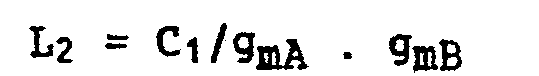
- the output impedance is an inductance L 2 defined by:
- a gyrator is, in a known state of the art, formed of two transconductive amplifiers, that is to say sources of current, voltage-controlled, of opposite transconductances, mounted head to tail in parallel.
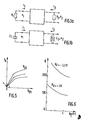
- This gyrator therefore comprises, as shown in FIG. 3a, an amplifier A and an inverting amplifier B.
- the gyration conductance g o is then linked to the conductances of each of the amplifiers, gmA and gmB respectively, by the relation:
- the capacitor C 1 connected to the input E of the gyrator circuit is then transformed into the inductance L 2
- the capacitance C 1 is lossless, the gyrator without losses, the admittance of gyration is real, and the inductance L 2 generated is then pure.
- the matrix is of the form: with for the currents i 1 and i 2 at the input and at the output as a function of the voltages v 1 and v 2 at the input and at the output as shown in FIG. 1a.
- the susceptible parts of the admittances y11 and y 22 of input and output of the gyrator, respectively jb 11 and jb 22 , are added to the susceptance of the load capacity Ci and to the output inductance L 2 , so that the latter are modified, in particular L 2 takes the value Lg.
- the total conductance is expressed by: relation in which g C is the conductance of the capacitor C 1 .
- g L is the conductance of the circuit at the terminals of which the inductance L 2 is mounted.
- the quality factor is controlled and the precision on the value of the inductance generated from a capacitance is obtained by controlling the phase shift ⁇ on the one hand and the inductance g 2 on the other go.
- FIG. 3b gives an equivalent block diagram of the circuit of FIG. 2.
- Part P 2 is an inverter stage, as well as parts P 1 and P 3 .
- Part P 4 is a buffer stage (in English BUFFER).
- the inverters P 1 and P 2 are in series with the stage buffer P 4 and are equivalent to a non-inverting amplifier such as A ( Figure 3a).
- the part P 3 is equivalent to the inverting amplifier B of FIG. 3a.
- these amplifiers are therefore of opposite polarity and mounted head to tail in parallel between nodes a and b.
- the capacitor C 1 placed at the input E, between the node a and the mass m is transformed by the gyrator into an inductance Lg placed between the node b and the mass m.
- the capacitor C 2 placed in parallel on Lg forms the resonant circuit LC sought.
- the signal to be filtered at frequency F, or any other signal for any other application, is applied to the gyrator device according to the invention at the input INP of an amplifier P A (see FIG. 3b).
- the filtered signal is collected on the output S (see figures 2, 3b, 3c).
- Each inverter stage Pt, P 2 , P 3 consists of an inverter transistor Tt, T 2 , T 3 and an active load T'i, T ' 2 , T' 3, respectively .
- Each stage is continuously isolated from the preceding and the following, by a capacitor, such as C 3 , C 4 , C 5 , C G , just as the input INP is by a capacitor C7.
- the transistors used to make the circuit according to the invention are preferably field effect transistors of the MESFET type which have advantageous properties in the production of circuits operating at high frequencies.
- the amplifier stages produced by means of these transistors usually show a very small gain, this gain being however improved in a known manner by the use of an active load.
- an active load has the advantage of providing a high dynamic load, which promotes the gain, the latter being proportional to the load, and of providing a lower continuous load, which does not not deteriorate the gain by too large a direct current.
- the use of the active load supposes a very delicate polarization of the two transistors connected in series, the inverter transistor and the load transistor, these two transistors each behaving like two current sources connected in series. In fact, in such an arrangement, the slightest difference in polarization can cause one or the other of these transistors to be desaturated.
- each inverting amplifier stage of the circuit the active load constituted by each of the transistors T 'is polarized as shown in FIG. 4a.
- the load transistor T ' is mounted as a common drain on the positive DC power supply V DD , its source is connected to the common drain point of the inverter transistor T and of output 0 of the inverter stage.
- the inverter transistor T is mounted so that its source is connected to ground, and its gate, on which the input I of the stage is applied, is polarized by a resistor R placed between 1 and a negative potential -V GG .
- the gate of the charge transistor T ' is polarized on the one hand by means of a resistor R' connected to a positive supply VA and on the other hand by means of a capacitor C 'connected to the point o.
- the voltage VA is taken from the common point between the resistor Rp and the level shift diode Dp, the resistor Rp being on the other hand connected to the voltage V DD and the diode Dp connected to ground.
- a voltage -V B defined by -V GG ⁇ -V B ⁇ 0 is calibrated by the same method as V A , that is to say with respect to the mass by a diode D S and with respect to -V GG by a resistor Rs (see FIG. 2).
- the reversing stage provided with such a load behaves as according to the circuit shown in FIG. 4b, that is to say as with a conventional active load.
- the inverter stage behaves as according to the circuit shown in FIG. 4c.
- the transistor T 'then behaves as a follower, that is to say that its source voltage follows the voltage V A. It is then, no longer a current source as before, but a voltage source, with a low output impedance.
- the inverter stage is then formed no longer of two current sources in series as it was known, but of a current source (T) in series with a voltage source (T '). The operation of each inverter stage is thus optimized.
- the stage Pi only includes as elements corresponding to the assembly described above that the elements T ' 1 , R' 1 , C ' 1 .
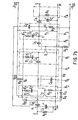
- the device according to the invention which makes it possible to control the phase shift introduced by the gyrator, comprises two parts denoted Ps and Ps, delimited in FIG. 2 by dotted lines. The part Ps is precisely applied to the gate of the transistor T 1 in the expected position for a resistor R 1 in accordance with the diagram in FIG. 4a.
- the part Ps of the phase shift control of the gyrator according to the invention consists of a transistor T d whose drain is connected to the gate of the transistor T 1 , whose source is connected to the voltage -V B and whose gate is brought to a control voltage V d (see FIG. 2).
- This voltage V d is provided such that the transistor T d works in an area where its drain current I D is close to zero (but equal to 0 continuously), for example in the delimited area Z by dotted lines in FIG. 5 which represents the characteristics I D as a function of the drain-source voltage V DS for different gate-source voltages V GS .
- the transistor T D operates in a region where the characteristics are linear and behaves like a variable resistor R d whose value is electrically controlled by the voltage Vd (see FIG. 3b).
- this resistor R d is located in parallel on the output S and makes it possible to act on the output conductance g 2 of the gyrator.
- the part P 6 also makes it possible to act on the phase shift 9 of the gyrator.
- the part P 4 of the gyrator consists of a buffer stage (in English BUFFER) formed by a transistor mounted as a drain common to V DD T 4 , and by a current source transistor T ' 4, the source and the grid of which are short-circuited are connected to ground.
- the part P 6 consists of a diode D ⁇ in series with a capacitor C ' ⁇ , this arrangement being placed between the common point of the transistors T 4 and T' 4 of the buffer stage and the ground.
- the set P 6 thus forms a C ⁇ variable capacitance whose value is a function of the ⁇ V control voltage applied to the common point between the diode D and the capacitor C ⁇ ' ⁇ .
- the term g 2 is controlled by the variable resistance R d . This resistance varies by producing an increase in the term g 2 which causes a decrease in the quality factor Q.
- variable capacitance C ⁇ acts by increasing the absolute value of the phase shift ⁇ therefore by increasing the quality factor Q.
- the amplifier P A on the INP input of which is applied the signal F to be filtered itself consists of an inverting amplifier stage.
- This stage comprises (see FIG. 2) a transistor T A , the charge of which is common to transistor T 3 , and which is biased with respect to the negative voltage -V GG via the resistor R A.
- This system makes it possible to produce the circuit by means of field effect transistors of the MESFET type, which is particularly advantageous for operation at high frequencies.
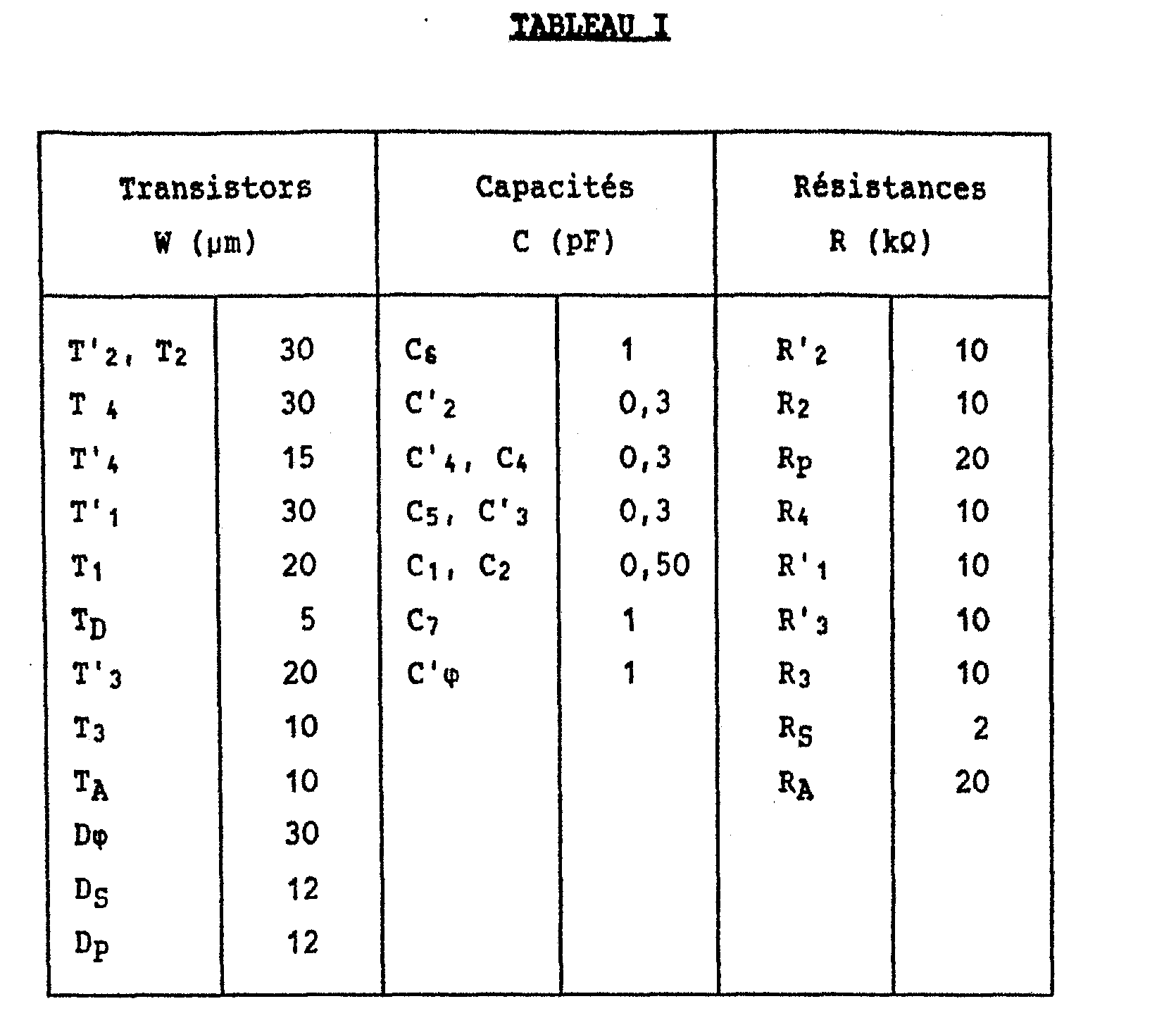
- the circuit according to the invention is made up of elements whose values are given in table I, where W is the gate width of the transistors, with: pinch tension
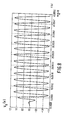
- FIG. 6 shows the values obtained for the quality factor Q as a function of the values of the control voltages V ⁇ and V d of the two adjustment elements of the gyrator according to the invention. On average, this quality factor is between 100 and 250.
- this monolithically integrated circuit on a group III-V material such as gallium arsenide for example. If it is produced by means of the elements whose characteristics are given in table I, it then occupies an area of approximately 0.25 mm 2, and can operate in a frequency range between 40 MHz and 2 kHz.
- this circuit can for other applications, and by providing suitable elements, be used on the contrary as an oscillator.
- the part P 6 of the circuit makes it possible to achieve the negative resistance necessary for the oscillation.
- the adjustment of the oscillation frequency is obtained by the simultaneous variation of the input and output capacities C 1 and C 2 which will advantageously be varicaps.
- the oscillation frequency is deduced from the relation: If L 2 was fixed, as is the case in an oscillator conventionally known to those skilled in the art, the oscillation frequency can be expressed by: where K 'is a constant. On the contrary according to the invention, since L 2 is adjustable, the oscillation frequency is expressed by: which represents a great advantage compared to the state of the art of the fact that one will easily obtain high oscillation frequencies with very small capacities. When you know that in the field of circuit integration, the area occupied by the capacitors poses a big problem, so that certain high-value capacitors cannot even be integrated, the advantage provided by the circuit according to the invention when used as an oscillator appears immediately.
- the oscillator according to the invention has still other advantages.
- the gyrator circuit used as an oscillator in which the transistors are field effect transistors of the MESFET type and of which all the components are very small. Besides the advantage of high frequencies, the circuit is very compact and consumes very little. The characteristics of this circuit are gathered in table II and the diagram of the oscillator circuit is represented on figure 7a.
- the control voltage V C makes it possible to change the value of the capacitors C 1 and C 2 , which are constituted by diodes D 1 and D 2 , and therefore the frequency. It will be noted that resistors R E and R S have been added in parallel on C 1 and C 2 and that insulation capacities CE and C S have also been added.
- Stage P5 can also be deleted.
- the circuit consumption is then 100 mW.
- the frequency band is from 2 GHz to 5 GHz.
- Figure 8 shows the oscillations obtained on the output signal V S (in V) as a function of time t, at 3 GHz.
- the stage P 4 is eliminated, all the transistors pass to 10 ⁇ m and the consumption to 40 mW. But the frequency band is slightly narrower and centered on 2.8 GHz-3.5 GHz.
Abstract
Description
- L'invention concerne un circuit gyrateur formé d'une part d'un premier et d'un second amplificateurs transconductifs, respectivement A et B, de transconductances opposées, montés en parallèle entre une première borne a et une seconde borne b, et formé d'autre part d'une première capacité C1 montée entre ladite première borne a et une troisième borne m, ce circuit gyrateur simulant une inductance Lg montée entre ladite deuxième borne b et ladite troisième borne m, et comprenant un moyen pour contrôler son facteur de qualité Q.
- L'invention concerne également un circuit résonnant incluant cette inductance Lg.
- L'invention trouve son application dans la réalisation de filtres hyperfréquences, ainsi que dans la réalisation d'oscillateurs.
- Un circuit gyrateur simulant une inductance et inclus dans un circuit résonnant à fonction de filtre est connu par la publication dans "IEEE, J. Solid-State Circuits, Vol. SC-15, pp 963-968, Dec. 1980", de l'article intitulé "Gyrator Video Filter IC with Automatic Tuning" par Kenneth W. MOULDING et alii. Ce document décrit un circuit gyrateur formé de deux amplificateurs différentiels, sources de courant, commandés en tension, de transconductances opposées, montés tête-bêche en parallèle, et chargé sur deux capacités. La technologie utilisée pour réaliser ce circuit inclut des transistors bipolaires dont la tension de seuil est telle qu'elle induit dans les amplificateurs un déphasage important qui se traduit par une résistance négative plus grande en valeur absolue que la résistance positive due aux pertes, risquant d'entraîner le circuit à osciller. Ce circuit est, pour cette raison, muni d'une résistance supplémentaire destinée à s'ajouter à la résistance positive due aux pertes, afin de compenser ce défaut et d'éviter l'oscillation. Le facteur de qualité d'un tel circuit étant inversement proportionnel à la résultante de la résistance due au déphasage et de la résistance due aux pertes, cette résistance supplémentaire doit donc être faible. Dans ce circuit connu cette résistance supplémentaire est placée en série avec l'une des capacités de charge du gyrateur et est reliée à une tension de polarisation destinée à permettre l'ajustement de l'accord du résonnateur.
- Mais ce circuit connu doit répondre à un impératif qui est de réaliser un circuit résonnant à une fréquence donnée faible, tout en présentant comme on l'a vu un bon facteur de qualité. Les difficultés rencontrées dans la mise en oeuvre de ce circuit proviennent de la dispersion des caractéristiques des composants et tout particulièrement de la réalisation des résistances.
- C'est pourquoi afin de rendre ce circuit indépendant des problèmes de dispersion de caractéristiques, un circuit gyrateur auxiliaire accordé sur un oscillateur à quartz, est utilisé pour accorder le gyrateur-filtre en fournissant la tension de polarisation des capacités. Ce système permet alors le contrôle en boucle fermée du circuit gyrateur auxiliaire, mais se fonde sur le fait que le gyrateur-filtre suit obligatoirement.
- Ce circuit connu présente, pour l'application au fonctionnement hyperfréquences envisagé, plusieurs inconvénients :
- - Tout d'abord la fréquence de fonctionnement est trop faible « 10 MHZ).
- - Ensuite la dispersion des caractéristiques et notamment celles des résistances entraîne la nécessité d'utiliser un gyrateur auxiliaire.
- - Enfin le gyrateur filtre est seulement piloté par le gyrateur auxiliaire mais non contrôlé.
- Or pour cette application envisagée, il est impératif que :
- - la fréquence de fonctionnement soit élevée, c'est-à-dire dans le domaine situé entre 2 KHz et 40 MHz,
- - le facteur de qualité soit élevé,
- - la fréquence de filtrage soit précise et les caractéristiques du circuit répétitives.
- Selon l'invention ce but est atteint au moyen d'un circuit tel que décrit dans le préambule, caractérisé en ce que le premier circuit amplificateur transconductif A est formé de deux étages amplificateurs inverseurs P, et F2 montés en série, en ce que le second circuit amplificateur transconductif B est formé d'un étage amplificateur inverseur P3, et en ce que le moyen pour contrôler le facteur de qualité Q est formé d'un premier moyen Ps pour agir sur la conductance de sortie g2 du gyrateur, et d'un second moyen P, pour agir sur le déphasage m entre le courant de sortie et la tension de commande du gyrateur.
- Ce circuit gyrateur présente alors entre autres les avantages suivants :
- - il est possible d'utiliser des FET en arséniure de gallium et donc d'atteindre des fréquences très élevées,
- - les deux paramètres principaux du circuit, à savoir la résistance positive due aux pertes et la résistance négative dûe au déphasage sont contrôlées, à la différence du dispositif connu où seulement un moyen pour agir sur la résistance due aux pertes était prévu,
- - le facteur de qualité est donc réellement contrôlé,
- - le facteur de qualité est alors très élevé, de l'ordre de 250,
- - le circuit est plus simple que le dispositif connu et il est entièrement intégrable.
- Dans l'application envisagée à un circuit résonnant pour former un filtre :
- - la fréquence de fonctionnement est alors très élevée, c'est-à-dire dans le domaine 2 Khz à 40 MHz,
- - la fréquence de filtrage est très précise,
- - les caractéristiques du circuit sont répétitives donc appropriées à une fabrication en grande série.
- Dans l'application envisagée à un oscillateur :
- - la bande de fréquence couverte est très large : 2 à 5 GHz;
- - le circuit est de faible surface et présente une très faible consommation car les transistors et les capacités doivent être choisis petits.
- L'invention sera mieux comprise au moyen de la description suivante illustrée par les figures annexées dont :
- - les figures 1a et 1b qui représentent les schémas équivalents d'un circuit gyrateur, respectivement dans le cas général et dans le cas où le gyrateur est chargé sur une capacité ;
- - la figure 2 qui représente le schéma électrique d'un filtre à circuit résonnant incluant un gyrateur selon l'invention ;
- - la figure 3a qui représente le schéma par blocs d'un circuit résonnant incluant un gyrateur correspondant au cas de la figure 1b ;
- - la figure 3b qui représente le schéma par bloc du filtre à circuit résonnant selon l'invention, correspondant à la figure 2 ;
- - la figure 4a qui représente le schéma électrique d'un étage amplificateur inverseur du gyrateur selon l'invention ;
- - les figures 4b et 4c qui représentent le schéma équivalent au schéma de la figure 4a respectivement en fonctionnement alternatif et en fonctionnement continu ;
- - la figure 5 qui montre sur son réseau de caractéristiques, la zone de fonctionnement du transistor Td utilisé comme résistance variable ;
- - la figure 6 qui représente, en fonction des tensions de commande du transistor Td utilisé comme résistance variable et de la diode Dw utilisée comme capacité variable, le facteur de qualité Q du gyrateur, dans un exemple de réalisation ;
- - les figures 7a et 7b qui représentent le circuit oscillateur selon l'invention dans deux exemples ;
- - la figure 8 qui représente la courbe d'oscillations en fonction du temps obtenue dans une mise en oeuvre de ce dernier circuit.
- Le problème se pose donc :
- - de filtrer une fréquence de 2 KHz à 40 MHz avec une grande précision,
- - au moyen d'un dispositif intégré présentant un facteur de qualité élevé,
- - au moyen d'un tel dispositif présentant une grande fiabilité tout en étant bon marché pour une application grand public.
- Ce but est atteint au moyen du gyrateur selon l'invention. On notera que selon les valeurs des caractéristiques des éléments utilisés pour réaliser ce circuit gyrateur, ce dernier peut évidemment être utilisé au filtrage d'autres fréquences ou comme oscillateur, ce qui sera exposé plus loin.
- Selon l'invention, comme selon le circuit considéré comme état de la technique, le circuit gyrateur proposé est utilisé pour simuler une inductance afin de réaliser un circuit résonnant formé de cette inductance notée ultérieurement L2 et d'une capacité C2.
- Selon le principe de fonctionnement des gyrateurs, illustré par le schéma équivalent d'un tel circuit, représenté sur la figure 1a, une admittance y1 placée à l'entrée est liée à l'admittance de sortie y2 par la relation :
- Y2 = g o 2/Y1
- Ainsi, si l'admittance d'entrée est une capacité Ci (figure 1b), l'impédance de sortie est une inductance L2 définie par :

- Un gyrateur est, de façon connue de l'état de la technique, formé de deux amplificateurs transconductifs, c'est-à-dire sources de courant, commandés en tension, de transconductances opposées, montés tête-bêche en parallèle. Ce gyrateur comporte donc, comme montré figure 3a, un amplificateur A et un amplificateur inverseur B. La conductance de gyration go est alors liée aux conductances de chacun des amplificateurs, gmA et gmB respectivement, par la relation :

- La capacité C1 connectée à l'entrée E du circuit gyrateur est alors transformée en l'inductance L2
- Dans le cas réel d'amplificateur non idéal, la matrice d'admittance complète de l'amplificateur est :

- Pour le gyrateur formé de deux amplificateurs comme il est dit plus haut, la matrice est de la forme :


- Les parties susceptives des admittances y11 et y22 d'entrée et de sortie du gyrateur, respectivement jb11 et jb22, s'ajoutent à la susceptance de la capacité de la charge Ci et à l'inductance de sortie L2, de sorte que ces dernières sont modifiées, en particulier L2 prend la valeur Lg.
- Les parties conductives des admittances y11 et Y22 vont entraîner une diminution du facteur de qualité de l'inductance.
- A l'entrée du gyrateur, la conductance totale s'exprime par :

- A la sortie du gyrateur la conductance s'exprime par

- En tenant compte du fait que le terme g, est très petit devant le terme ωC1, et que le déphasage ϕ/2, défini par ϕ = Arg(-y21.y12) est petit, (c'est-à-dire cos ϕ = 1, et sin ϕ * ϕ), l'effet des deux conductances g1 et g2 se traduit par l'admittance de sortie :


- Le courant de sortie d'un amplificateur transconductif est en retard par rapport à la tension de commande donc ϕ < 0 et ce déphasage introduit une augmentation du facteur de qualité.
- Selon la présente invention, le facteur de qualité est contrôlé et la précision sur la valeur de l'inductance générée à partir d'une capacité est obtenue par le contrôle du déphasage ϕ d'une part et de l'inductance g2 d'autre part.
- Tel que représenté sur la figure 2, le circuit gyrateur selon l'invention comprend plusieurs parties délimitées par des pointillés. La figure 3b donne un schéma équivalent par blocs du circuit de la figure 2.
- La partie P2 est un étage inverseur, ainsi que les parties P1 et P3. La partie P4 est un étage tampon (en anglais BUFFER).
- Les inverseurs P1 et P2 sont en série avec l'étage tampon P4 et sont équivalents à un amplificateur non inverseur tel que A (figure 3a). La partie P3 est équivalente à l'amplificateur inverseur B de la figure 3a. Comme le montre cette même figure, ces amplificateurs sont donc de polarité opposée et montés tête-bêche en parallèle entre les noeuds a et b.
- La capacité C1 placée à l'entrée E, entre le noeud a et la masse m est transformée par le gyrateur en une inductance Lg placée entre le noeud b et la masse m. La capacité C2 placée en parallèle sur Lg forme le circuit résonnant LC recherché.
- Le signal à filtrer à la fréquence F, ou tout autre signal pour toute autre application, est appliqué au dispositif gyrateur selon l'invention à l'entrée INP d'un amplificateur PA (voir figure 3b). Le signal filtré est recueilli sur la sortie S (voir figures 2, 3b, 3c).
- Chaque étage inverseur Pt, P2, P3 est constitué d'un transistor inverseur respectivement Tt, T2, T3 et d'une charge active T'i, T'2, T'3. Chaque étage est isolé du précédent et du suivant en continu, par une capacité, telle que C3, C4, C5, CG, de même que l'entrée INP l'est par une capacité C7.
- Les charges actives de chacun des étages inverseurs présentent une structure particulière par ailleurs connue du brevet US 4 241 316 pour une application totalement différente.
- Cette structure est ici appliquée dans le but d'améliorer les performances de chaque étage inverseur en tant qu'amplificateur. En effet les transistors utilisés pour réaliser le circuit selon l'invention sont de préférence des transistors à effet de champ du type MESFET qui présentent des propriétés avantageuses dans la réalisation de circuits fonctionnant à des fréquences élevées. Les étages amplificateurs réalisés au moyen de ces transistors montrent habituellement un gain très faible, ce gain étant cependant amélioré d'une façon connue par l'utilisation d'une charge active.
- En effet, l'utilisation d'une charge active présente l'avantage de fournir une charge élevée en dynamique, ce qui favorise le gain, ce dernier étant proportionnel à la charge, et de fournir une charge plus faible en continu, ce qui ne détériore pas le gain par un trop grand courant continu.
- Cependant l'utilisation de la charge active suppose une polarisation très délicate des deux transistors montés en série, le transistor inverseur et le transistor charge, ces deux transistors se comportant chacun comme deux sources de courant montées en série. En effet, dans un tel montage, le moindre écart de polarisation peut faire en sorte que l'un ou l'autre de ces transistors se trouve déssaturé.
- C'est pourquoi dans chaque étage amplificateur inverseur du circuit selon l'invention, la charge active constituée par chacun des transistors T' est polarisée comme montrée figure 4a. Le transistor de charge T' est monté en drain commun sur l'alimentation continue positive VDD, sa source est reliée au point commun de drain du transistor inverseur T et de sortie 0 de l'étage inverseur. Le transistor inverseur T est monté de telle sorte que sa source est reliée à la masse, et sa grille, sur laquelle l'entrée I de l'étage est appliquée, est polarisée par une résistance R placée entre 1 et un potentiel négatif -VGG. La grille du transistor de charge T' est polarisée d'une part au moyen d'une résistance R' reliée à une alimentation positive VA et d'autre part au moyen d'une capacité C' reliée au point o.
- L'étage étant alimenté par les alimentations continues constituées par la masse, VDD et -VGG, l'alimentation continue VA est calée par rapport à ces alimentations. La tension VA est prélevée au point commun entre la résistance Rp et la diode Dp de décalage de niveau, la résistance Rp étant d'autre part reliée à la tension VDD et la diode Dp reliée à la masse. Spécifiquement pour les étages P1 et P2, une tension -VB définie par -VGG < -VB < 0 est calée par la même méthode que VA, c'est-à-dire par rapport à la masse par une diode DS et par rapport à -VGG par une résistance Rs (voir figure 2).
- En fonctionnement, on peut considérer qu'en alternatif l'étage inverseur muni d'une telle charge se comporte comme selon le circuit représenté figure 4b, c'est-à-dire comme avec une charge active conventionnelle.
- En continu par contre, on peut considérer que l'étage inverseur se comporte comme selon le circuit représenté figure 4c. Le transistor T' se comporte alors en suiveur, c'est-à-dire que sa tension de source suit la tension VA. C'est alors, non plus une source de courant comme précédemment, mais une source de tension, avec une impédance de sortie faible. L'étage inverseur est alors formé non plus de deux sources de courant en série comme il était connu, mais d'une source de courant (T) en série avec une source de tension (T'). Le fonctionnement de chaque étage inverseur se trouve ainsi optimisé. On retrouve les éléments T', R', C', R dans chaque étage respectivement T'2, R'2, C'2, R2 pour P1, T'3, R'3, C'3, R3 Pour P3. Mais l'étage Pi ne comprend comme éléments correspondants au montage décrit précédemment que les éléments T'1, R'1, C'1. En effet le dispositif selon l'invention, qui permet de contrôler le déphasage introduit par le gyrateur, comprend deux parties notées Ps et Ps, délimitées sur la figure 2 par des pointillés. La partie Ps est précisément appliquée sur la grille du transistor T1 dans la position attendue pour une résistance R1 en conformité avec le schéma de la figure 4a.
- La partie Ps du contrôle du déphasage du gyrateur selon l'invention consiste en un transistor Td dont le drain est relié à la grille du transistor T1, dont la source est reliée à la tension -VB et dont la grille est portée à une tension de commande Vd (voir figure 2). Cette tension Vd est prévue telle que le transistor Td travaille dans une zone où son courant de drain ID est voisin de zéro (mais égale à 0 en continu), par exemple dans la zone Z délimitée par des pointillés sur la figure 5 qui représente les caractéristiques ID en fonction de la tension drain-source VDS pour différentes tensions grille-source VGS.
- Dans ces conditions le transistor TD fonctionne dans une région où les caractéristiques sont linéaires et se comporte comme une résistance variable Rd dont la valeur est commandée électriquement par la tension Vd (voir figure 3b).
- En fonctionnement en courant alternatif, cette résistance Rd se trouve en parallèle sur la sortie S et permet d'agir sur la conductance de sortie g2 du gyrateur.
- La partie P6 permet d'autre part d'agir sur le déphasage 9 du gyrateur. Comme il est montré sur la figure 2, la partie P4 du gyrateur consiste en un étage tampon (en anglais BUFFER) formé d'un transistor monté en drain commun à VDD T4, et d'un transistor source de courant T'4 dont la source et la grille court-circuitées sont reliées à la masse. La partie P6 est constituée d'une diode Dϕ en série avec une capacité C'ϕ, ce montage étant placé entre le point commun des transistors T4 et T'4 de l'étage tampon et la masse. L'ensemble P6 forme ainsi une capacité variable Cϕ dont la valeur est fonction de la tension de commande Vϕ appliquée au point commun entre la diode Dϕ et la capacité C'ϕ.
- En reprenant l'équation (1) qui donne le facteur de qualité du gyrateur, le terme g2 est contrôlé par la résistance variable Rd. Cette résistance varie en produisant une augmentation du terme g2 qui provoque une diminution du facteur de qualité Q.
- D'autre part, en considérant encore cette équation (1), la capacité variable Cϕ agit en augmentant la valeur absolue du déphasage ϕ donc en augmentant le facteur de qualité Q.
- Ces actions s'équilibrent pour permettre le contrôle absolu des éléments et des caractéristiques du gyrateur selon l'invention.
- L'amplificateur PA sur l'entrée INP duquel est appliqué le signal F à filtrer, est constitué lui-même d'un étage amplificateur inverseur. Cet étage comprend (voir figure 2) un transistor TA dont la charge est commune au transistor T3, et qui est polarisé par rapport à la tension négative -VGG par l'intermédiaire de la résistance RA.
- Ce système permet de réaliser le circuit au moyen de transistors à effet de champ du type MESFET, particulièrement avantageux pour le fonctionnement à fréquences élevées.
- Dans un exemple de réalisation d'un gyrateur pour l'application au filtrage, le circuit selon l'invention est formé d'éléments dont les valeurs sont reportées dans le tableau I, où W est la largeur de grille des transistors, avec :


- VT = - 2,5 V pour tous les transistors et la largeur de la grille :
- 1 = 0,7um pour tous les transistors.
- La figure 6 montre les valeurs obtenues pour le facteur de qualité Q en fonction des valeurs des tensions de commande Vϕ et Vd des deux éléments d'ajustage du gyrateur selon l'invention. En moyenne ce facteur de qualité est situé entre 100 et 250.
- L'ensemble de ce circuit monolithiquement intégrable sur un matériau du groupe III-V tel que l'arséniure de gallium par exemple. S'il est réalisé au moyen des éléments dont les caractéristiques sont données dans le tableau I, il occupe alors une surface d'environ 0,25 mm2, et peut fonctionner dans un domaine de fréquences entre 40 MHz et 2 kHz.
- Les paramètres ϕ et g2 du circuit selon l'invention étant totalement contrôlables, ce circuit peut pour d'autres applications, et en prévoyant des éléments appropriés, être utilisé au contraire comme oscillateur. Dans cette application la partie P6 du circuit permet de réaliser la résistance négative nécessaire à l'oscillation. Le réglage de la fréquence d'oscillation est obtenu par la variation simultanée des capacités d'entrée et sortie C1 et C2 qui seront de façon avantageuse des varicaps.
- Dans ce cas les capacités de gyration et d'accord C1 = C2 sont toujours les mêmes. Leur valeur est choisie de manière à obtenir le facteur
- 1/Q < 0 sur toute la bande de fréquences d'oscillation.
- Une des particularités de cette variante de l'invention est que l'amplificateur PA de sortie est supprimé par rapport au circuit gyrateur représenté sur la figure 2, et sur la figure 3a.
- On sait que pour un oscillateur la fréquence d'oscillation se déduit de la relation :


- L'oscillateur selon l'invention présente encore d'autres avantages. Notamment, on sait que pour obtenir un coefficient de surtension élevé, les amplificateurs à trans- conductance doivent obligatoirement n'introduire que de faibles pertes. Cette condition est remplie dès lors que les transistors sont choisis de petites tailles (9d très petit).
- La self impédance simulée par le gyrateur selon l'invention et dont la valeur est donnée par :

- Donc dans une mise en oeuvre de l'invention, des fréquences très élevées sont obtenues par le circuit gyrateur utilisé comme oscillateur dans lequel les transistors sont des transistors à effet de champ du type MESFET et dont tous les composants sont très petits. Outre l'avantage des fréquences élevées, le circuit est très compact et consomme très peu. Les caractéristiques de ce circuit sont rassemblées dans le tableau II et le schéma du circuit oscillateur est représenté sur la figure 7a.

- La tension de commande VC permet de changer la valeur des capacités C1 et C2, qui sont constituées par des diodes D1 et D2, et donc la fréquence. On notera que des résistances RE et RS ont été rajoutées en parallèle sur C1 et C2 et que des capacités d'isolement CE et CS ont également été rajoutées.
- L'étage P5 peut également être supprimé. La consommation du circuit est alors de 100 mW. La bande de fréquence est de 2 GHz à 5 GHz. La figure 8 montre les oscillations obtenues sur le signal de sortie VS (en V) en fonction du temps t, à 3 GHz.
- Dans une autre variante du gyrateur utilisé comme oscillateur et représenté sur la figure 7b, l'étage P4 est supprimé, tous les transistors passent à 10 um et la consommation à 40 mW. Mais la bande de fréquence est légèrement moins large et centrée sur 2,8 GHz-3,5 GHz.
Claims (14)
Applications Claiming Priority (2)
| Application Number | Priority Date | Filing Date | Title |
|---|---|---|---|
| FR8611032A FR2602380B1 (fr) | 1986-07-30 | 1986-07-30 | Circuit gyrateur simulant une inductance |
| FR8611032 | 1986-07-30 |
Publications (1)
| Publication Number | Publication Date |
|---|---|
| EP0256580A1 true EP0256580A1 (fr) | 1988-02-24 |
Family
ID=9337877
Family Applications (1)
| Application Number | Title | Priority Date | Filing Date |
|---|---|---|---|
| EP87201397A Withdrawn EP0256580A1 (fr) | 1986-07-30 | 1987-07-21 | Circuit gyrateur simulant une inductance |
Country Status (5)
| Country | Link |
|---|---|
| US (1) | US4812785A (fr) |
| EP (1) | EP0256580A1 (fr) |
| JP (1) | JPS6338317A (fr) |
| KR (1) | KR880002322A (fr) |
| FR (1) | FR2602380B1 (fr) |
Cited By (3)
| Publication number | Priority date | Publication date | Assignee | Title |
|---|---|---|---|---|
| EP0365091A2 (fr) * | 1988-10-21 | 1990-04-25 | Philips Electronics Uk Limited | Montage de filtre |
| FR2763681A1 (fr) * | 1997-05-26 | 1998-11-27 | Canon Kk | Dispositif de determination d'une quantite de produit consommable presente dans un reservoir et dispositif d'impression de documents correspondant |
| DE102014008990A1 (de) | 2014-06-13 | 2015-12-17 | Dietmar Dreyer | Halbleiterverstärker zur Speicherung von elektrischer Energie auf der Basis eines generierten Schwingkreises |
Families Citing this family (42)
| Publication number | Priority date | Publication date | Assignee | Title |
|---|---|---|---|---|
| GB2208340B (en) * | 1987-07-17 | 1992-01-22 | Plessey Co Plc | Electrical circuits |
| JP2784467B2 (ja) * | 1987-12-04 | 1998-08-06 | 日本電信電話株式会社 | 電圧制御発振器 |
| EP0398728B1 (fr) * | 1989-05-19 | 1994-07-13 | Murata Manufacturing Co., Ltd. | Dispositif capteur électrostatique du type céramique à résonance |
| JPH04284005A (ja) * | 1991-03-13 | 1992-10-08 | Sharp Corp | 発振回路 |
| US5287036A (en) * | 1992-03-02 | 1994-02-15 | Motorola, Inc. | Method and apparatus for acoustic wave inductance |
| JPH05283972A (ja) * | 1992-04-03 | 1993-10-29 | Nec Corp | フィルタ回路 |
| US5347238A (en) * | 1993-07-06 | 1994-09-13 | Trw Inc. | Bipolar microwave monolithic voltage controlled oscillator using active inductors |
| KR19990035935A (ko) * | 1996-05-28 | 1999-05-25 | 엠. 제이. 엠. 반캄 | 전기 통신 장치용 부속 장치 |
| US5850163A (en) * | 1997-03-31 | 1998-12-15 | Sun Microsystems, Inc. | Active inductor oscillator with wide frequency range |
| KR19990057175A (ko) * | 1997-12-29 | 1999-07-15 | 김영환 | 자이레이터를 이용한 임피던스 정합장치 |
| US6104230A (en) * | 1998-09-16 | 2000-08-15 | Conexant Systems, Inc. | Electronic inductor circuit using cascoded transistors |
| US6184747B1 (en) | 1999-05-13 | 2001-02-06 | Honeywell International Inc. | Differential filter with gyrator |
| US6236238B1 (en) | 1999-05-13 | 2001-05-22 | Honeywell International Inc. | Output buffer with independently controllable current mirror legs |
| US7015789B1 (en) * | 1999-05-13 | 2006-03-21 | Honeywell International Inc. | State validation using bi-directional wireless link |
| US6727816B1 (en) | 1999-05-13 | 2004-04-27 | Honeywell International Inc. | Wireless system with variable learned-in transmit power |
| US6901066B1 (en) | 1999-05-13 | 2005-05-31 | Honeywell International Inc. | Wireless control network with scheduled time slots |
| US6429733B1 (en) | 1999-05-13 | 2002-08-06 | Honeywell International Inc. | Filter with controlled offsets for active filter selectivity and DC offset control |
| DE19958096B4 (de) * | 1999-12-02 | 2012-04-19 | Telefonaktiebolaget Lm Ericsson (Publ) | Verfahren zum Entwerfen einer Filterschaltung |
| US6583661B1 (en) | 2000-11-03 | 2003-06-24 | Honeywell Inc. | Compensation mechanism for compensating bias levels of an operation circuit in response to supply voltage changes |
| US7826373B2 (en) * | 2005-01-28 | 2010-11-02 | Honeywell International Inc. | Wireless routing systems and methods |
| US8085672B2 (en) * | 2005-01-28 | 2011-12-27 | Honeywell International Inc. | Wireless routing implementation |
| US7742394B2 (en) * | 2005-06-03 | 2010-06-22 | Honeywell International Inc. | Redundantly connected wireless sensor networking methods |
| US7848223B2 (en) * | 2005-06-03 | 2010-12-07 | Honeywell International Inc. | Redundantly connected wireless sensor networking methods |
| US8463319B2 (en) * | 2005-06-17 | 2013-06-11 | Honeywell International Inc. | Wireless application installation, configuration and management tool |
| US7394782B2 (en) * | 2005-07-14 | 2008-07-01 | Honeywell International Inc. | Reduced power time synchronization in wireless communication |
| US7801094B2 (en) * | 2005-08-08 | 2010-09-21 | Honeywell International Inc. | Integrated infrastructure supporting multiple wireless devices |
| US20070030816A1 (en) * | 2005-08-08 | 2007-02-08 | Honeywell International Inc. | Data compression and abnormal situation detection in a wireless sensor network |
| US7289466B2 (en) * | 2005-10-05 | 2007-10-30 | Honeywell International Inc. | Localization for low cost sensor network |
| US7603129B2 (en) * | 2005-10-05 | 2009-10-13 | Honeywell International Inc. | Localization identification system for wireless devices |
| US8811231B2 (en) * | 2005-10-21 | 2014-08-19 | Honeywell International Inc. | Wireless transmitter initiated communication systems |
| US8644192B2 (en) * | 2005-10-21 | 2014-02-04 | Honeywell International Inc. | Wireless transmitter initiated communication methods |
| US20070097873A1 (en) * | 2005-10-31 | 2007-05-03 | Honeywell International Inc. | Multiple model estimation in mobile ad-hoc networks |
| US8285326B2 (en) * | 2005-12-30 | 2012-10-09 | Honeywell International Inc. | Multiprotocol wireless communication backbone |
| US8413227B2 (en) * | 2007-09-28 | 2013-04-02 | Honeywell International Inc. | Apparatus and method supporting wireless access to multiple security layers in an industrial control and automation system or other system |
| US7986701B2 (en) * | 2008-06-13 | 2011-07-26 | Honeywell International Inc. | Wireless building control system bridge |
| US8884198B2 (en) * | 2010-01-22 | 2014-11-11 | Continental Automotive Systems, Inc. | Parametric temperature regulation of induction heated load |
| US8365703B2 (en) * | 2010-01-22 | 2013-02-05 | Continental Automotive Systems Us, Inc. | Switch-mode synthetic power inductor |
| US9115908B2 (en) | 2011-07-27 | 2015-08-25 | Honeywell International Inc. | Systems and methods for managing a programmable thermostat |
| US9157764B2 (en) | 2011-07-27 | 2015-10-13 | Honeywell International Inc. | Devices, methods, and systems for occupancy detection |
| US9621371B2 (en) | 2012-07-24 | 2017-04-11 | Honeywell International Inc. | Wireless sensor device with wireless remote programming |
| GB2532043B (en) | 2014-11-06 | 2021-04-14 | Honeywell Technologies Sarl | Methods and devices for communicating over a building management system network |
| US10753902B2 (en) * | 2018-10-01 | 2020-08-25 | International Business Machines Corporation | Chipless and wireless sensor circuit and sensor tag |
Citations (6)
| Publication number | Priority date | Publication date | Assignee | Title |
|---|---|---|---|---|
| DE1487484A1 (de) * | 1966-11-07 | 1969-04-30 | Siemens Ag | Erdunsymmetrischer UEbertragungs-Vierpol |
| US3597698A (en) * | 1969-07-07 | 1971-08-03 | Gen Telephone & Elect | Integratable gyrator |
| US3624537A (en) * | 1969-07-07 | 1971-11-30 | Gte Laboratories Inc | Gyrator network |
| US3643183A (en) * | 1970-05-19 | 1972-02-15 | Westinghouse Electric Corp | Three-amplifier gyrator |
| US3840829A (en) * | 1973-02-02 | 1974-10-08 | E Hochmair | Integrated p-channel mos gyrator |
| US3921102A (en) * | 1973-07-23 | 1975-11-18 | Philips Corp | Circuit arrangement including a gyrator resonant circuit |
Family Cites Families (1)
| Publication number | Priority date | Publication date | Assignee | Title |
|---|---|---|---|---|
| US3715693A (en) * | 1972-03-20 | 1973-02-06 | J Fletcher | Gyrator employing field effect transistors |
-
1986
- 1986-07-30 FR FR8611032A patent/FR2602380B1/fr not_active Expired
-
1987
- 1987-07-21 EP EP87201397A patent/EP0256580A1/fr not_active Withdrawn
- 1987-07-24 US US07/077,572 patent/US4812785A/en not_active Expired - Fee Related
- 1987-07-27 JP JP62185629A patent/JPS6338317A/ja active Pending
- 1987-07-27 KR KR1019870008140A patent/KR880002322A/ko not_active Application Discontinuation
Patent Citations (6)
| Publication number | Priority date | Publication date | Assignee | Title |
|---|---|---|---|---|
| DE1487484A1 (de) * | 1966-11-07 | 1969-04-30 | Siemens Ag | Erdunsymmetrischer UEbertragungs-Vierpol |
| US3597698A (en) * | 1969-07-07 | 1971-08-03 | Gen Telephone & Elect | Integratable gyrator |
| US3624537A (en) * | 1969-07-07 | 1971-11-30 | Gte Laboratories Inc | Gyrator network |
| US3643183A (en) * | 1970-05-19 | 1972-02-15 | Westinghouse Electric Corp | Three-amplifier gyrator |
| US3840829A (en) * | 1973-02-02 | 1974-10-08 | E Hochmair | Integrated p-channel mos gyrator |
| US3921102A (en) * | 1973-07-23 | 1975-11-18 | Philips Corp | Circuit arrangement including a gyrator resonant circuit |
Cited By (6)
| Publication number | Priority date | Publication date | Assignee | Title |
|---|---|---|---|---|
| EP0365091A2 (fr) * | 1988-10-21 | 1990-04-25 | Philips Electronics Uk Limited | Montage de filtre |
| EP0365091A3 (fr) * | 1988-10-21 | 1991-01-02 | Philips Electronics Uk Limited | Montage de filtre |
| FR2763681A1 (fr) * | 1997-05-26 | 1998-11-27 | Canon Kk | Dispositif de determination d'une quantite de produit consommable presente dans un reservoir et dispositif d'impression de documents correspondant |
| EP0881475A1 (fr) * | 1997-05-26 | 1998-12-02 | Canon Kabushiki Kaisha | Dispositifpour la détermination de la quantité d'un produit consommable present dans un réservoir et dispositf correspondant d'impression des documents |
| US6310635B1 (en) | 1997-05-26 | 2001-10-30 | Canon Kabushiki Kaisha | Device for determining a quantity of consumable product present in a reservoir and corresponding device for printing documents |
| DE102014008990A1 (de) | 2014-06-13 | 2015-12-17 | Dietmar Dreyer | Halbleiterverstärker zur Speicherung von elektrischer Energie auf der Basis eines generierten Schwingkreises |
Also Published As
| Publication number | Publication date |
|---|---|
| KR880002322A (ko) | 1988-04-30 |
| FR2602380B1 (fr) | 1988-10-21 |
| FR2602380A1 (fr) | 1988-02-05 |
| US4812785A (en) | 1989-03-14 |
| JPS6338317A (ja) | 1988-02-18 |
Similar Documents
| Publication | Publication Date | Title |
|---|---|---|
| EP0256580A1 (fr) | Circuit gyrateur simulant une inductance | |
| EP0283074B1 (fr) | Mélangeur hyperfréquences | |
| CH633670B5 (fr) | Circuit oscillateur a onde rectangulaire pour la mesure du temps. | |
| EP1265352B1 (fr) | Circuit oscillateur différentiel comprenant un résonateur électromécanique | |
| EP0321329B1 (fr) | Oscillateur doubleur de fréquence accordé par varactors | |
| EP1916762B1 (fr) | Oscillateur à quartz asservi en amplitude avec domaine étendu de tension et de température | |
| EP0660512B1 (fr) | Amplificateur déphaseur et son application à un circuit recombineur | |
| EP3416284B1 (fr) | Architecture de partage de tension entre deux oscillateurs | |
| FR2905041A1 (fr) | Circuit de capacite negative pour applications hautes frequences | |
| EP1424776A1 (fr) | Circuit oscillateur commandé en tension pour un dispositif électronique basse puissance | |
| FR2532115A1 (fr) | Circuit comprenant un element a transconductance variable | |
| EP0150140A2 (fr) | Circuit de polarisation d'un transistor à effet de champ | |
| EP0549043B1 (fr) | Circuit intégré comprenant un amplificateur à gain variable | |
| FR2589652A1 (fr) | Dispositif semi-conducteur du type melangeur | |
| EP0859458B1 (fr) | Circuit de modulation de fréquence d'un oscillateur à quartz | |
| EP1081848B1 (fr) | Dispositif de transposition de fréquence à faible fuite de signal d'oscillateur local et procédé correspondant de réduction de fuite | |
| FR2549314A1 (fr) | Quadrupole d'adaptation, independante de la frequence de fonctionnement, d'une reactance, et amplificateur a ondes progressives utilisant un tel quadrupole | |
| FR2730363A1 (fr) | Amplificateur a gain eleve en hautes frequences et oscillateur a circuit resonant muni d'un tel amplificateur | |
| FR2622752A1 (fr) | Circuit formant un filtre actif r.c. pour application coupe-bande | |
| EP0596562A1 (fr) | Dispositif comprenant un circuit pour traiter un signal alternatif | |
| EP0061421A1 (fr) | Circuit intégré pour oscillateur à fréquence réglable | |
| EP0347985B1 (fr) | Circuit actif hyperfréquences du type passe-tout | |
| FR2625052A1 (fr) | Circuit hyperfrequences comprenant au moins un transistor a effet de champ charge | |
| EP1569332B1 (fr) | Circuit d'amplification de puissance et amplificateur operationnel l'incorporant | |
| EP1276226B1 (fr) | Circuit destiné à générer une conductance négative substantiellement constante en fonction de la fréquence |
Legal Events
| Date | Code | Title | Description |
|---|---|---|---|
| PUAI | Public reference made under article 153(3) epc to a published international application that has entered the european phase |
Free format text: ORIGINAL CODE: 0009012 |
|
| AK | Designated contracting states |
Kind code of ref document: A1 Designated state(s): DE FR GB IT NL |
|
| 17P | Request for examination filed |
Effective date: 19880713 |
|
| RAP1 | Party data changed (applicant data changed or rights of an application transferred) |
Owner name: N.V. PHILIPS' GLOEILAMPENFABRIEKEN Owner name: LABORATOIRES D'ELECTRONIQUE PHILIPS |
|
| 17Q | First examination report despatched |
Effective date: 19900910 |
|
| STAA | Information on the status of an ep patent application or granted ep patent |
Free format text: STATUS: THE APPLICATION IS DEEMED TO BE WITHDRAWN |
|
| 18D | Application deemed to be withdrawn |
Effective date: 19911126 |
|
| RIN1 | Information on inventor provided before grant (corrected) |
Inventor name: PAUKER, VLAD |