EP0257955A2 - Chemical sensor - Google Patents
Chemical sensor Download PDFInfo
- Publication number
- EP0257955A2 EP0257955A2 EP87307273A EP87307273A EP0257955A2 EP 0257955 A2 EP0257955 A2 EP 0257955A2 EP 87307273 A EP87307273 A EP 87307273A EP 87307273 A EP87307273 A EP 87307273A EP 0257955 A2 EP0257955 A2 EP 0257955A2
- Authority
- EP
- European Patent Office
- Prior art keywords
- chemically
- plasmon resonance
- surface plasmon
- layer
- sensitive surface
- Prior art date
- Legal status (The legal status is an assumption and is not a legal conclusion. Google has not performed a legal analysis and makes no representation as to the accuracy of the status listed.)
- Withdrawn
Links
Images


Classifications
-
- G—PHYSICS
- G01—MEASURING; TESTING
- G01N—INVESTIGATING OR ANALYSING MATERIALS BY DETERMINING THEIR CHEMICAL OR PHYSICAL PROPERTIES
- G01N21/00—Investigating or analysing materials by the use of optical means, i.e. using sub-millimetre waves, infrared, visible or ultraviolet light
- G01N21/75—Systems in which material is subjected to a chemical reaction, the progress or the result of the reaction being investigated
- G01N21/77—Systems in which material is subjected to a chemical reaction, the progress or the result of the reaction being investigated by observing the effect on a chemical indicator
- G01N21/7703—Systems in which material is subjected to a chemical reaction, the progress or the result of the reaction being investigated by observing the effect on a chemical indicator using reagent-clad optical fibres or optical waveguides
- G01N21/774—Systems in which material is subjected to a chemical reaction, the progress or the result of the reaction being investigated by observing the effect on a chemical indicator using reagent-clad optical fibres or optical waveguides the reagent being on a grating or periodic structure
- G01N21/7743—Systems in which material is subjected to a chemical reaction, the progress or the result of the reaction being investigated by observing the effect on a chemical indicator using reagent-clad optical fibres or optical waveguides the reagent being on a grating or periodic structure the reagent-coated grating coupling light in or out of the waveguide
-
- G—PHYSICS
- G01—MEASURING; TESTING
- G01N—INVESTIGATING OR ANALYSING MATERIALS BY DETERMINING THEIR CHEMICAL OR PHYSICAL PROPERTIES
- G01N21/00—Investigating or analysing materials by the use of optical means, i.e. using sub-millimetre waves, infrared, visible or ultraviolet light
- G01N21/17—Systems in which incident light is modified in accordance with the properties of the material investigated
- G01N21/55—Specular reflectivity
- G01N21/552—Attenuated total reflection
- G01N21/553—Attenuated total reflection and using surface plasmons
Definitions
- This invention relates to a chemical sensor and it relates particularly to a chemically-sensitive surface plasmon resonance device.
- SPR Surface plasmon resonance
- Figure 1 of the accompanying drawings shows a known SPR configuration, referred to as "Kretschmann's Arrangement", which comprises a glass prism 1 with a thin metal layer 2 attached to one face of the prism. Attainment of a resonance condition depends on a number of operational and constructional parameters.
- layer 2 is 30nm thick and is made of silver and the prism has a refractive index of 1.517. Assuming operation in air, surface plasmons can be excited in the metal layer if light at a wavelength of 633 nm (i.e. He-Ne laser light) is incident at the glass/metal interface 3 at an angle ⁇ r of 43°.
- a resonance absorption due to excitation of plasmons in metal layer 2, can be observed as a sharp dip in the intensity of light reflected at the interface as a function of incidence angle.
- the shape and angular position of the dip are found to be extremely sensitive to the dielectric properties of the medium immediately adjacent to the exposed surface of layer 2, remote from the prism, and this fact has been exploited in a chemical sensor.
- a system based on Kretschmann's Arrangement can be used as an immunosensor and, in an example, an immune specific protein (biotin) was immobilised by silane coupling at the exposed surface of layer 2 by means of an intervening coating of silicon dioxide which acts as an adhesion aid.
- the immobilised layer was then incubated with the appropriate target molecule in solution (avidin) producing a detectable shift in the resonance absorption curve. This shift is shown in Figure 3.
- a chemically-sensitive surface plasmon resonance device comprising a slab of a light-transmissive material being flat on one side and having a plurality of formations on the opposite side, a layer of a metal formed on said one side of the slab and a layer of a chemically-sensitive material formed on, or in the vicinity of, said metal layer, whereby, in use, white light incident on said formations undergoes reflection at the interface of said one side and said metal layer and, after reflection, undergoes dispersion as the light leaves said opposite side and in a resonance condition of the device, exposure of said chemically-sensitive material to an analyte causes a detectable change, as a function of the wavelength of the reflected light, of the position of a plasmon resonance absorption.
- a device in accordance with the present invention exhibits a variation of reflectivity as a function of wavelength.
- a collimated beam of white light i.e. light containing a range of wavelengths in the visible part of the spectrum
- This wavelength can be identified by focussing the dispersed beam at an image plane and scanning a response characteristic of a suitable detection system relative to the spectrally dispersed image. Such scanning could be accomplished electrically by interrogating the outputs of an array of charge coupled devices, for example, thereby eliminating the need for mechanical movement of a precedm whether for the purpose of calibrating the device or identifying the resonance condition.
- a chemically-sensitive surface plasmon resonance system comprising a chemically-sensitive surface plasmon resonance device according to said first aspect of the invention, a source for producing a collimated beam of white light incident on said opposite side, means to focus, at an image plane, a dispersed beam exitant from said opposite side and detection means having a response characteristic which can be scanned electrically relative to said image plane.
- Said slab which constitutes an optical component of the device may be made from any of a number of commercially available, optical quality materials, and devices may be manufactured in quantity, at low cost, by employing planar processing techniques.
- a metal layer and, if desired, a chemically-sensitive layer may be formed by suitable deposition techniques on a suitably moulded sheet of said optical quality material containing a plurality of optical components, the sheet then being sectioned to separate individual devices.
- Figure 1 illustrates a SPR system, known to those skilled in the art as Kretschmann's Arrangement
- Figure 2 shows a plot of reflectivity against angle of incidence produced using the system of Figure 1
- Figure 3 shows two plots of reflectivity against angle of incidence produced using an immunosensor based on the system of Figure 1
- Figure 4 shows a chemically-sensitive system in accordance with the present invention
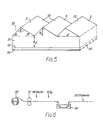
- Figure 5 shows a cross-sectional view through a device used in the system of Figure 4
- Figure 6 illustrates a possible process for manufacturing a device in accordance with the invention.
- a chemically-sensitive surface plasmon resonance system comprises a chemically-sensitive surface plasmon resonance device, shown generally at 10, a source 20 of white light in combination with a lens system 21 designed to produce a collimated beam B incident on the device and a further lens system 22 designed to focus a dispersed beam D at an image plane I.
- the device 10 comprises a generally rectangular slab 11 of a suitable optical quality mouldable material.
- the material used should be of a uniform, isotropic composition, should have an appropriate refractive index commersurate with achieving the plasmon resonance condition and should be readily fabricated. Suitable materials include thermoplastics materials, perspex, cold cure epoxy and glass.
- the slab is flat on one side 12 and is formed with a number of parallel, evenly spaced ridges 13 on the opposite side.
- the ridges which are generally triangular, in cross-section are defined by respective pairs of flat, mutually inclined surfaces (e.g. S).
- the angles ⁇ , ⁇ , ⁇ subtended by respective sides of the ridges may be chosen to achieve a desired degree of refraction or dispersion as required by a particular application.
- the pitch d of the ridges might be 0.1mm, the depth h1 of the ridges being typically 0.1mm and the depth h2 of the slab being about 1mm. It will be understood, however, that different dimensions, consistent with achieving dispersion, could be used, and the ridges need not necessarily be spaced apart from one another evenly nor need they be precisely triangular.
- Side 12 of the slab carries a thin reflective layer 14 of a suitable metal (eg Ag) in which surface plasmons are to be excited and a layer 15 of a chemically-sensitive material may be deposited on the metal layer on the side thereof remote from the slab.
- the chemically-sensitive material is chosen to respond to a desired analyte which is arranged to pass through a cell 23, as shown in Figure 4.
- the response of the chemically-sensitive material causes a change of dielectric property, and so refractive index, of the environment immediately adjacent to layer 14 and, as described hereinbefore, this change produces a detectable shift in the position of maximum resonance absorption as a function of the wavelength of reflected light.
- layer 15 may comprise an appropriate chemisorbent, absorbent or adsorbent coating. If the analyte comprises ions in solution, layer 15 may comprise an electro-active membrane e.g. glass, PVC/valinomycin (for K+ions). Alternatively, if the device is to be used as a immunosensor, immunologically active molecules of a suitable antibody/antigen may be immobilised on layer 14 by means of a suitable adhesion aid such as silicon dioxide. In an alternative arrangement layer 15 may be formed as an enzyme substrate 26 on wall 25 of cell 23, as shown, to define a narrow channel in the cell along which the analyte may pass. In this case the enzyme is chosen to convert the analyte to a product which causes a change of bulk refractive index of the analyte solution, detectable as a shift in the position of the maximum resonance absorption.
- the enzyme is chosen to convert the analyte to a product which causes a change of bulk refractive index of the analyte solution, detect
- the collimated beam B is incident at right angles to respective parallel surfaces of ridges 13.
- the beam is reflected at the interface of slab 11 and metal layer 14 and is then dispersed as it exits from the slab to form the dispersed beam D which is focussed at image plane I.
- the dispersed beam D which is focussed at image plane I.
- Only two wavelengths are represented in Figure 4.
- This wavelength can be identified by scanning a response characteristic of a detection system 24 relative to the spectrally dispersed image of source 20 formed at the image plane thereby to detect the resonance absorption maximum.
- Such scanning can be achieved electrically using any of a number of known detection systems e.g. CCD photodiode array, vidicon tube. It is possible, therefore, to calibrate the sensor against any desired reference without recourse to mechanical adjustment demanded in the prior arrangements described hereinbefore.
- the reflectance spectrum, scanned by the detection system may be analysed numerically thereby to monitor changes in the shape and/or position of the resonance absorption curve caused by exposure of the chemically-sensitive material to an analyte under test. This object may be assisted by generating a second, reference reflectance spectrum by treating one half only of layer 14 with the chemical-sensitive material.
- optical component 10 is advantageous in that it can be readily manufactured in quantity and at low cost.
- a large number of components may be manufactured as a single sheet, up to 250 mm x 250 mm in area say, by conventional techniques - hot moulding in the case of a thermoplastics material or solution casting over a former in the case of perspex, for example.
- Metallic and chemically-sensitive layers are applied to the sheet, as desired, by suitable planar processing techniques and the sheet is then sectioned to produce individual devices each in the size range from 5 mm x 5 mm to 20 mm x 20 mm, say. Thus, as many as 2500 individual devices could be processed simultaneously.
- Devices could be manufactured by means of a "continuous" process illustrated schematically in Figure 6.
- a strip of a flexible, optical quality material would be fed from a reel 30 through suitably shaped, heated rollers 31 to impress the strip with a pattern of ridges (13 in Figure 5).
- a metal layer is then deposited, by evaporation, for example, on the plain side of the strip followed, if desired, by deposition of an adhesion aid (e.g. Si02) by sputtering for example.
- an adhesion aid e.g. Si02
- the treated strip would be passed through a bath 32 containing a silanising agent (to promote antibody coupling) prior to sectioning the strip to separate the individual devices.
- a device in accordance with the present invention can be used to monitor a wide range of chemical properties including ion activity and concentration, presence and concentration of enzymes, substrates, antibodies, antigens, haptens, hormones and reducible gases, and the presence, concentration and activity of any of a variety of chemical and biochemical substances in the gaseous phase and in solution.
- the analyte is remote from the light beam and this can be advantageous in the case of an opaque solution such as blood which might otherwise interfere with reflectivity measurements.
Landscapes
- Physics & Mathematics (AREA)
- Chemical & Material Sciences (AREA)
- General Health & Medical Sciences (AREA)
- Health & Medical Sciences (AREA)
- Life Sciences & Earth Sciences (AREA)
- Analytical Chemistry (AREA)
- Biochemistry (AREA)
- General Physics & Mathematics (AREA)
- Immunology (AREA)
- Pathology (AREA)
- Chemical Kinetics & Catalysis (AREA)
- Plasma & Fusion (AREA)
- Engineering & Computer Science (AREA)
- Investigating Or Analysing Materials By Optical Means (AREA)
- Investigating Or Analysing Materials By The Use Of Chemical Reactions (AREA)
Abstract
Description
- This invention relates to a chemical sensor and it relates particularly to a chemically-sensitive surface plasmon resonance device.
- Surface plasmon resonance (SPR) can arise when photons are reflected at a dielectric/metal interface under conditions such that the momentum of the photons becomes coupled to the electron gas in the metal thereby exciting collective longitudinal oscillations known as plasmons.
- Figure 1 of the accompanying drawings shows a known SPR configuration, referred to as "Kretschmann's Arrangement", which comprises a glass prism 1 with a thin metal layer 2 attached to one face of the prism. Attainment of a resonance condition depends on a number of operational and constructional parameters. In an example, layer 2 is 30nm thick and is made of silver and the prism has a refractive index of 1.517. Assuming operation in air, surface plasmons can be excited in the metal layer if light at a wavelength of 633 nm (i.e. He-Ne laser light) is incident at the glass/
metal interface 3 at an angle ϑr of 43°. - As illustrated in Figure 2 of the drawings a resonance absorption, due to excitation of plasmons in metal layer 2, can be observed as a sharp dip in the intensity of light reflected at the interface as a function of incidence angle. The shape and angular position of the dip are found to be extremely sensitive to the dielectric properties of the medium immediately adjacent to the exposed surface of layer 2, remote from the prism, and this fact has been exploited in a chemical sensor.
- In experiments described by Nylander, Liedberg and Lind in "Sensors and Actuators" Vol 7 1982 p79, Kretschmann's Arrangement was used to detect a halogenated hydrocarbon gas, halothane. A thin film of silicone-glycol copolymer, an oil which reversibly absorbs halothane, was applied to the exposed surface of metal layer 2. Absorption of the gas produced a change in the dielectric properties of the oil which, in turn, gave rise to a detectable shift in the angular position of the resonance absorption, the extent of the shift being related linearly to the concentration of gas absorbed, at least over a limited range of concentrations.
- Similarly, a system based on Kretschmann's Arrangement can be used as an immunosensor and, in an example, an immune specific protein (biotin) was immobilised by silane coupling at the exposed surface of layer 2 by means of an intervening coating of silicon dioxide which acts as an adhesion aid. The immobilised layer was then incubated with the appropriate target molecule in solution (avidin) producing a detectable shift in the resonance absorption curve. This shift is shown in Figure 3.
- It will be apparent, therefore, that by application of a suitable chemically-sensitive film it is possible to monitor the presence and/or concentration of a wide range of analytes both in the gaseous phase and in solution.
- In practice, it is convenient to monitor reflectivity at a fixed angle of incidence. However, because the shape and angular position of the resonance absorption depends critically on the characteristics (e.g. thickness, composition) of materials deposited on the prixm, a sensor of the kind described hereinbefore would need to be carefully calibrated, possibly against standard references, and the angle of incidence may need to be re-adjusted prior to each new measurement. Both of these procedures would necessitate some form of mechanical movement arranged to rotate the prism relative to the laser and a detector adding to the mechanical complexity and cost of the system and tending to reduce overall reliability and ease of use.
- It is an object of the present invention to provide a chemical sensor based on the SPR technique which at least alleviates the above-mentioned problems associated with calibration and adjustment of the system and which is amenable to reliable manufacturing techniques consistent with large scale commercial production.
- According to a first aspect of the invention there is provided a chemically-sensitive surface plasmon resonance device comprising a slab of a light-transmissive material being flat on one side and having a plurality of formations on the opposite side, a layer of a metal formed on said one side of the slab and a layer of a chemically-sensitive material formed on, or in the vicinity of, said metal layer,
whereby, in use, white light incident on said formations undergoes reflection at the interface of said one side and said metal layer and, after reflection, undergoes dispersion as the light leaves said opposite side and in a resonance condition of the device, exposure of said chemically-sensitive material to an analyte causes a detectable change, as a function of the wavelength of the reflected light, of the position of a plasmon resonance absorption. - It will be appreciated that in contrast to prior devices which exhibit a variation of reflectivity as a function of incidence angle a device in accordance with the present invention exhibits a variation of reflectivity as a function of wavelength. By arranging that a collimated beam of white light (i.e. light containing a range of wavelengths in the visible part of the spectrum) is incident at said interface at an angle which is approximately commensurate with the resonance condition it will always be possible, in principle, to find a wavelength in the dispersed beam which is precisely consistent with achieving the maximum resonance absorption condition. This wavelength can be identified by focussing the dispersed beam at an image plane and scanning a response characteristic of a suitable detection system relative to the spectrally dispersed image. Such scanning could be accomplished electrically by interrogating the outputs of an array of charge coupled devices, for example, thereby eliminating the need for mechanical movement of a prixm whether for the purpose of calibrating the device or identifying the resonance condition.
- According to another aspect of the invention there is provided a chemically-sensitive surface plasmon resonance system comprising a chemically-sensitive surface plasmon resonance device according to said first aspect of the invention, a source for producing a collimated beam of white light incident on said opposite side, means to focus, at an image plane, a dispersed beam exitant from said opposite side and detection means having a response characteristic which can be scanned electrically relative to said image plane.
- Said slab which constitutes an optical component of the device may be made from any of a number of commercially available, optical quality materials, and devices may be manufactured in quantity, at low cost, by employing planar processing techniques. A metal layer and, if desired, a chemically-sensitive layer may be formed by suitable deposition techniques on a suitably moulded sheet of said optical quality material containing a plurality of optical components, the sheet then being sectioned to separate individual devices.
- In order that the invention may be carried readily into effect an embodiment thereof is now described in detail, by way of example only, by reference to Figures 4 to 6 of the accompanying drawings of which, Figure 1 illustrates a SPR system, known to those skilled in the art as Kretschmann's Arrangement, Figure 2 shows a plot of reflectivity against angle of incidence produced using the system of Figure 1, Figure 3 shows two plots of reflectivity against angle of incidence produced using an immunosensor based on the system of Figure 1, Figure 4 shows a chemically-sensitive system in accordance with the present invention, Figure 5 shows a cross-sectional view through a device used in the system of Figure 4, and Figure 6 illustrates a possible process for manufacturing a device in accordance with the invention.
- Referring to Figure 4, a chemically-sensitive surface plasmon resonance system comprises a chemically-sensitive surface plasmon resonance device, shown generally at 10, a
source 20 of white light in combination with alens system 21 designed to produce a collimated beam B incident on the device and a further lens system 22 designed to focus a dispersed beam D at an image plane I. - Referring now to Figure 5, the
device 10 comprises a generallyrectangular slab 11 of a suitable optical quality mouldable material. The material used should be of a uniform, isotropic composition, should have an appropriate refractive index commersurate with achieving the plasmon resonance condition and should be readily fabricated. Suitable materials include thermoplastics materials, perspex, cold cure epoxy and glass. The slab is flat on oneside 12 and is formed with a number of parallel, evenlyspaced ridges 13 on the opposite side. In this example, the ridges, which are generally triangular, in cross-section are defined by respective pairs of flat, mutually inclined surfaces (e.g. S). The angles α, β, γ subtended by respective sides of the ridges may be chosen to achieve a desired degree of refraction or dispersion as required by a particular application. - Typically the pitch d of the ridges might be 0.1mm, the depth h₁ of the ridges being typically 0.1mm and the depth h₂ of the slab being about 1mm. It will be understood, however, that different dimensions, consistent with achieving dispersion, could be used, and the ridges need not necessarily be spaced apart from one another evenly nor need they be precisely triangular.
-
Side 12 of the slab carries a thinreflective layer 14 of a suitable metal (eg Ag) in which surface plasmons are to be excited and alayer 15 of a chemically-sensitive material may be deposited on the metal layer on the side thereof remote from the slab. The chemically-sensitive material is chosen to respond to a desired analyte which is arranged to pass through acell 23, as shown in Figure 4. The response of the chemically-sensitive material causes a change of dielectric property, and so refractive index, of the environment immediately adjacent tolayer 14 and, as described hereinbefore, this change produces a detectable shift in the position of maximum resonance absorption as a function of the wavelength of reflected light. - If the analyte is a gas or vapour,
layer 15 may comprise an appropriate chemisorbent, absorbent or adsorbent coating. If the analyte comprises ions in solution,layer 15 may comprise an electro-active membrane e.g. glass, PVC/valinomycin (for K⁺ions). Alternatively, if the device is to be used as a immunosensor, immunologically active molecules of a suitable antibody/antigen may be immobilised onlayer 14 by means of a suitable adhesion aid such as silicon dioxide. In analternative arrangement layer 15 may be formed as anenzyme substrate 26 onwall 25 ofcell 23, as shown, to define a narrow channel in the cell along which the analyte may pass. In this case the enzyme is chosen to convert the analyte to a product which causes a change of bulk refractive index of the analyte solution, detectable as a shift in the position of the maximum resonance absorption. - Numerous examples of other suitable chemically-sensitive materials will be readily envisaged by persons of ordinary skill in the art.
- Referring to Figure 4, the collimated beam B is incident at right angles to respective parallel surfaces of
ridges 13. The beam is reflected at the interface ofslab 11 andmetal layer 14 and is then dispersed as it exits from the slab to form the dispersed beam D which is focussed at image plane I. For clarity of illustration, only two wavelengths are represented in Figure 4. By arranging that beam B is incident at the interface at an angle which is approximately commersurate with a resonance condition it will always be possible, in principle, to find one wavelength in the dispersed beam which is precisely consistent with achieving the maximum resonance absorption condition. This wavelength can be identified by scanning a response characteristic of adetection system 24 relative to the spectrally dispersed image ofsource 20 formed at the image plane thereby to detect the resonance absorption maximum. Such scanning can be achieved electrically using any of a number of known detection systems e.g. CCD photodiode array, vidicon tube. It is possible, therefore, to calibrate the sensor against any desired reference without recourse to mechanical adjustment demanded in the prior arrangements described hereinbefore. Moreover, with the aid of suitable processing circuits the reflectance spectrum, scanned by the detection system, may be analysed numerically thereby to monitor changes in the shape and/or position of the resonance absorption curve caused by exposure of the chemically-sensitive material to an analyte under test. This object may be assisted by generating a second, reference reflectance spectrum by treating one half only oflayer 14 with the chemical-sensitive material. - Quite apart from its dispersive function,
optical component 10 is advantageous in that it can be readily manufactured in quantity and at low cost. Initially, a large number of components may be manufactured as a single sheet, up to 250 mm x 250 mm in area say, by conventional techniques - hot moulding in the case of a thermoplastics material or solution casting over a former in the case of perspex, for example. Metallic and chemically-sensitive layers are applied to the sheet, as desired, by suitable planar processing techniques and the sheet is then sectioned to produce individual devices each in the size range from 5 mm x 5 mm to 20 mm x 20 mm, say. Thus, as many as 2500 individual devices could be processed simultaneously. - Devices could be manufactured by means of a "continuous" process illustrated schematically in Figure 6. In this case, a strip of a flexible, optical quality material would be fed from a
reel 30 through suitably shaped, heatedrollers 31 to impress the strip with a pattern of ridges (13 in Figure 5). A metal layer is then deposited, by evaporation, for example, on the plain side of the strip followed, if desired, by deposition of an adhesion aid (e.g. Si0₂) by sputtering for example. If appropriate the treated strip would be passed through abath 32 containing a silanising agent (to promote antibody coupling) prior to sectioning the strip to separate the individual devices. - It will be appreciated that with a suitable choice of chemically-sensitive material a device in accordance with the present invention can be used to monitor a wide range of chemical properties including ion activity and concentration, presence and concentration of enzymes, substrates, antibodies, antigens, haptens, hormones and reducible gases, and the presence, concentration and activity of any of a variety of chemical and biochemical substances in the gaseous phase and in solution. Moreover, the analyte is remote from the light beam and this can be advantageous in the case of an opaque solution such as blood which might otherwise interfere with reflectivity measurements.
Claims (11)
whereby, in use, white light incident on said formations undergoes reflection at the interface of said one side and said metal layer and, after reflection, undergoes dispersion as the light leaves said opposite side and in a resonance condition of the device, exposure of said chemically-sensitive material to an analyte causes a detectable change, as a function of the wavelength of the reflected light, of the position of a plasmon resonance absorption.
Applications Claiming Priority (2)
| Application Number | Priority Date | Filing Date | Title |
|---|---|---|---|
| GB868620193A GB8620193D0 (en) | 1986-08-19 | 1986-08-19 | Chemical sensor |
| GB8620193 | 1986-08-19 |
Publications (2)
| Publication Number | Publication Date |
|---|---|
| EP0257955A2 true EP0257955A2 (en) | 1988-03-02 |
| EP0257955A3 EP0257955A3 (en) | 1989-04-12 |
Family
ID=10602931
Family Applications (1)
| Application Number | Title | Priority Date | Filing Date |
|---|---|---|---|
| EP87307273A Withdrawn EP0257955A3 (en) | 1986-08-19 | 1987-08-18 | Chemical sensor |
Country Status (3)
| Country | Link |
|---|---|
| EP (1) | EP0257955A3 (en) |
| JP (1) | JPS6375542A (en) |
| GB (1) | GB8620193D0 (en) |
Cited By (21)
| Publication number | Priority date | Publication date | Assignee | Title |
|---|---|---|---|---|
| EP0343826A1 (en) * | 1988-05-20 | 1989-11-29 | AMERSHAM INTERNATIONAL plc | Biological sensors |
| WO1990005295A1 (en) * | 1988-11-10 | 1990-05-17 | Pharmacia Ab | Optical biosensor system |
| WO1990008318A1 (en) * | 1989-01-11 | 1990-07-26 | Plessey Overseas Limited | Improvements in or relating to optical biosensors |
| WO1990011510A1 (en) * | 1989-03-23 | 1990-10-04 | Amersham International Plc | Assay method using surface plasmon resonance spectrometry |
| WO1991013339A1 (en) * | 1990-03-02 | 1991-09-05 | Fisons Plc | Sample cell for use in chemical or biochemical assays |
| WO1992001217A1 (en) * | 1990-07-04 | 1992-01-23 | Valtion Teknillinen Tutkimuskeskus | Method for carrying out surface plasmon resonance measurement and sensor for use in the method |
| DE4024476C1 (en) * | 1990-08-02 | 1992-02-27 | Boehringer Mannheim Gmbh, 6800 Mannheim, De | |
| EP0478137A2 (en) * | 1990-09-26 | 1992-04-01 | Gec-Marconi Limited | An optical sensor |
| WO1993014392A1 (en) * | 1992-01-11 | 1993-07-22 | Fisons Plc | Analytical device with polychromatic light source |
| US5474815A (en) * | 1993-10-01 | 1995-12-12 | Eastman Kodak Company | Production of carriers for surface plasmon resonance |
| WO1997001087A1 (en) * | 1995-06-23 | 1997-01-09 | Novartis Ag | Flow cell |
| US5776785A (en) * | 1996-12-30 | 1998-07-07 | Diagnostic Products Corporation | Method and apparatus for immunoassay using fluorescent induced surface plasma emission |
| DE19805809A1 (en) * | 1998-02-12 | 1999-09-02 | Biotul Bio Instr Gmbh | Transducer for determining surface plasmon resonances using spatially or time-modified layers for surface plasmon resonance spectroscopy |
| US5955153A (en) * | 1993-10-01 | 1999-09-21 | Johnson & Johnson Clinical Diagnostics, Inc. | Production of carriers for surface plasmon resonance |
| WO2001042768A1 (en) * | 1999-12-07 | 2001-06-14 | The Secretary Of State For Defence | Surface plasmon resonance |
| DE19615366B4 (en) * | 1996-04-19 | 2006-02-09 | Carl Zeiss Jena Gmbh | Method and device for detecting physical, chemical, biological or biochemical reactions and interactions |
| EP1307728B1 (en) * | 2000-08-09 | 2010-03-10 | Artificial Sensing Instruments ASI AG | Waveguide grid array and optical measurement arrangement |
| WO2011081847A1 (en) * | 2009-12-30 | 2011-07-07 | Maven Technologies, Llc. | Biological testing with a substrate having a bottom surface including sawtooth - shaped prisms |
| US8405638B2 (en) | 2009-12-22 | 2013-03-26 | Empire Technology Development Llc | Sensor system and optical touch sensor |
| US9291567B2 (en) | 2011-03-15 | 2016-03-22 | Lidija Malic | Microfluidic system having monolithic nanoplasmonic structures |
| DE102021100321A1 (en) | 2021-01-11 | 2022-07-14 | Leibniz-Institut für Ostseeforschung | SPR sensor unit and method for determining the refractive index of a sample medium and measuring device for detecting the density of a measuring medium |
Families Citing this family (1)
| Publication number | Priority date | Publication date | Assignee | Title |
|---|---|---|---|---|
| JPWO2014021171A1 (en) * | 2012-07-30 | 2016-07-21 | コニカミノルタ株式会社 | Method for manufacturing sensor member, method for manufacturing sensor chip, and method for using sensor member |
Citations (2)
| Publication number | Priority date | Publication date | Assignee | Title |
|---|---|---|---|---|
| US3279307A (en) * | 1963-01-21 | 1966-10-18 | Barnes Eng Co | Spectrum examination of substances |
| EP0255302A2 (en) * | 1986-07-25 | 1988-02-03 | ARS Holding 89 N.V. | Improvements relating to spectrometers |
-
1986
- 1986-08-19 GB GB868620193A patent/GB8620193D0/en active Pending
-
1987
- 1987-08-17 JP JP20323287A patent/JPS6375542A/en active Pending
- 1987-08-18 EP EP87307273A patent/EP0257955A3/en not_active Withdrawn
Patent Citations (2)
| Publication number | Priority date | Publication date | Assignee | Title |
|---|---|---|---|---|
| US3279307A (en) * | 1963-01-21 | 1966-10-18 | Barnes Eng Co | Spectrum examination of substances |
| EP0255302A2 (en) * | 1986-07-25 | 1988-02-03 | ARS Holding 89 N.V. | Improvements relating to spectrometers |
Non-Patent Citations (1)
| Title |
|---|
| SENSORS AND ACTUATORS, vol. 3, 1982/83, pages 79-89, Elsevier Sequoia, Amsterdam, NL; C. NYLANDER et al.: "Gas detection by means of surface plasmon resonance" * |
Cited By (29)
| Publication number | Priority date | Publication date | Assignee | Title |
|---|---|---|---|---|
| EP0343826A1 (en) * | 1988-05-20 | 1989-11-29 | AMERSHAM INTERNATIONAL plc | Biological sensors |
| US5313264A (en) * | 1988-11-10 | 1994-05-17 | Pharmacia Biosensor Ab | Optical biosensor system |
| WO1990005295A1 (en) * | 1988-11-10 | 1990-05-17 | Pharmacia Ab | Optical biosensor system |
| WO1990008318A1 (en) * | 1989-01-11 | 1990-07-26 | Plessey Overseas Limited | Improvements in or relating to optical biosensors |
| WO1990011510A1 (en) * | 1989-03-23 | 1990-10-04 | Amersham International Plc | Assay method using surface plasmon resonance spectrometry |
| WO1991013339A1 (en) * | 1990-03-02 | 1991-09-05 | Fisons Plc | Sample cell for use in chemical or biochemical assays |
| WO1992001217A1 (en) * | 1990-07-04 | 1992-01-23 | Valtion Teknillinen Tutkimuskeskus | Method for carrying out surface plasmon resonance measurement and sensor for use in the method |
| US5322798A (en) * | 1990-07-04 | 1994-06-21 | Valtion Teknillinen Tutkimuskeskus | Method for carrying out surface plasmon resonance measurement and sensor for use in the method |
| DE4024476C1 (en) * | 1990-08-02 | 1992-02-27 | Boehringer Mannheim Gmbh, 6800 Mannheim, De | |
| US5229833A (en) * | 1990-09-26 | 1993-07-20 | Gec-Marconi Limited | Optical sensor |
| EP0478137A3 (en) * | 1990-09-26 | 1993-01-13 | Gec-Marconi Limited | An optical sensor |
| EP0478137A2 (en) * | 1990-09-26 | 1992-04-01 | Gec-Marconi Limited | An optical sensor |
| WO1993014392A1 (en) * | 1992-01-11 | 1993-07-22 | Fisons Plc | Analytical device with polychromatic light source |
| US5474815A (en) * | 1993-10-01 | 1995-12-12 | Eastman Kodak Company | Production of carriers for surface plasmon resonance |
| US5955153A (en) * | 1993-10-01 | 1999-09-21 | Johnson & Johnson Clinical Diagnostics, Inc. | Production of carriers for surface plasmon resonance |
| WO1997001087A1 (en) * | 1995-06-23 | 1997-01-09 | Novartis Ag | Flow cell |
| DE19615366B4 (en) * | 1996-04-19 | 2006-02-09 | Carl Zeiss Jena Gmbh | Method and device for detecting physical, chemical, biological or biochemical reactions and interactions |
| US5776785A (en) * | 1996-12-30 | 1998-07-07 | Diagnostic Products Corporation | Method and apparatus for immunoassay using fluorescent induced surface plasma emission |
| DE19805809A1 (en) * | 1998-02-12 | 1999-09-02 | Biotul Bio Instr Gmbh | Transducer for determining surface plasmon resonances using spatially or time-modified layers for surface plasmon resonance spectroscopy |
| DE19805809C2 (en) * | 1998-02-12 | 2000-02-17 | Biotul Bio Instr Gmbh | Determination of the surface plasmon resonance using locally or temporally modified layers |
| WO2001042768A1 (en) * | 1999-12-07 | 2001-06-14 | The Secretary Of State For Defence | Surface plasmon resonance |
| US6753188B2 (en) | 1999-12-07 | 2004-06-22 | The Secretary Of State For Defence In Her Britannic Majesty's Government Of The United Kingdom Of Great Britain And Northern Ireland | Surface plasmon resonance |
| EP1307728B1 (en) * | 2000-08-09 | 2010-03-10 | Artificial Sensing Instruments ASI AG | Waveguide grid array and optical measurement arrangement |
| US8405638B2 (en) | 2009-12-22 | 2013-03-26 | Empire Technology Development Llc | Sensor system and optical touch sensor |
| WO2011081847A1 (en) * | 2009-12-30 | 2011-07-07 | Maven Technologies, Llc. | Biological testing with a substrate having a bottom surface including sawtooth - shaped prisms |
| US8355133B2 (en) | 2009-12-30 | 2013-01-15 | Maven Technologies, Llc | Biological testing with sawtooth-shaped prisms |
| US9291567B2 (en) | 2011-03-15 | 2016-03-22 | Lidija Malic | Microfluidic system having monolithic nanoplasmonic structures |
| DE102021100321A1 (en) | 2021-01-11 | 2022-07-14 | Leibniz-Institut für Ostseeforschung | SPR sensor unit and method for determining the refractive index of a sample medium and measuring device for detecting the density of a measuring medium |
| DE102021100321B4 (en) | 2021-01-11 | 2024-02-29 | Leibniz-Institut für Ostseeforschung | SPR sensor unit and method for determining the refractive index of a sample medium and measuring device for detecting the density of a measuring medium |
Also Published As
| Publication number | Publication date |
|---|---|
| GB8620193D0 (en) | 1986-10-01 |
| JPS6375542A (en) | 1988-04-05 |
| EP0257955A3 (en) | 1989-04-12 |
Similar Documents
| Publication | Publication Date | Title |
|---|---|---|
| EP0257955A2 (en) | Chemical sensor | |
| EP0346016B1 (en) | Biological sensors | |
| US6100991A (en) | Near normal incidence optical assaying method and system having wavelength and angle sensitivity | |
| EP0205236B1 (en) | Improvements in or relating to optic-waveguide biosensors | |
| US4815843A (en) | Optical sensor for selective detection of substances and/or for the detection of refractive index changes in gaseous, liquid, solid and porous samples | |
| EP1088231B1 (en) | Optical sensor having optimized surface profile | |
| US4997278A (en) | Biological sensors | |
| Thirstrup et al. | Diffractive optical coupling element for surface plasmon resonance sensors | |
| US5491556A (en) | Analytical device with variable angle of incidence | |
| EP0543831B1 (en) | Analytical device | |
| US20080037022A1 (en) | Surface Plasmon Resonance Sensor | |
| WO1999009396A1 (en) | Diffraction anomaly sensor having grating coated with protective dielectric layer | |
| JP2001066248A (en) | Surface plasmon sensor | |
| JPH06300683A (en) | Process and device for measuring propagation characteristic | |
| Slavík et al. | Advanced biosensing using simultaneous excitation of short and long range surface plasmons | |
| Goddard et al. | Real-time biomolecular interaction analysis using the resonant mirror sensor | |
| US20070109541A1 (en) | Differential surface plasmon resonance measuring device and its measuring method | |
| WO1993014392A1 (en) | Analytical device with polychromatic light source | |
| US7420682B2 (en) | Sensor device for interference and plasmon-waveguide/interference spectroscopy | |
| EP1308714B1 (en) | Measuring plate for a sensor utilising attenuated total reflection | |
| Fattinger et al. | Bidiffractive grating coupler: universal transducer for optical interface analytics | |
| WO1993014393A1 (en) | Analytical device with light scattering | |
| JPH09257699A (en) | Surface plasmon resonance sensor apparatus | |
| ZHANG et al. | Design and development of long range surface plasmon resonance sensor chip and system for high sensitivity detection | |
| WO2000045154A1 (en) | Coupled mode optical sensor |
Legal Events
| Date | Code | Title | Description |
|---|---|---|---|
| PUAI | Public reference made under article 153(3) epc to a published international application that has entered the european phase |
Free format text: ORIGINAL CODE: 0009012 |
|
| AK | Designated contracting states |
Kind code of ref document: A2 Designated state(s): AT BE CH DE ES FR GB GR IT LI LU NL SE |
|
| RIN1 | Information on inventor provided before grant (corrected) |
Inventor name: WEBB, BRIAN CHRISTOPHER Inventor name: DANIELS, PHELIM BRINLEY |
|
| RAP1 | Party data changed (applicant data changed or rights of an application transferred) |
Owner name: AMERSHAM INTERNATIONAL PLC |
|
| PUAL | Search report despatched |
Free format text: ORIGINAL CODE: 0009013 |
|
| RHK1 | Main classification (correction) |
Ipc: G01N 21/75 |
|
| AK | Designated contracting states |
Kind code of ref document: A3 Designated state(s): AT BE CH DE ES FR GB GR IT LI LU NL SE |
|
| STAA | Information on the status of an ep patent application or granted ep patent |
Free format text: STATUS: THE APPLICATION IS DEEMED TO BE WITHDRAWN |
|
| 18D | Application deemed to be withdrawn |
Effective date: 19891013 |
|
| RIN1 | Information on inventor provided before grant (corrected) |
Inventor name: WEBB, BRIAN CHRISTOPHER Inventor name: DANIELS, PHELIM BRINLEY |