EP0261897A2 - Display device - Google Patents
Display device Download PDFInfo
- Publication number
- EP0261897A2 EP0261897A2 EP87308310A EP87308310A EP0261897A2 EP 0261897 A2 EP0261897 A2 EP 0261897A2 EP 87308310 A EP87308310 A EP 87308310A EP 87308310 A EP87308310 A EP 87308310A EP 0261897 A2 EP0261897 A2 EP 0261897A2
- Authority
- EP
- European Patent Office
- Prior art keywords
- display
- lattice
- elements
- bit
- output
- Prior art date
- Legal status (The legal status is an assumption and is not a legal conclusion. Google has not performed a legal analysis and makes no representation as to the accuracy of the status listed.)
- Granted
Links
Images

Classifications
-
- G—PHYSICS
- G09—EDUCATION; CRYPTOGRAPHY; DISPLAY; ADVERTISING; SEALS
- G09G—ARRANGEMENTS OR CIRCUITS FOR CONTROL OF INDICATING DEVICES USING STATIC MEANS TO PRESENT VARIABLE INFORMATION
- G09G3/00—Control arrangements or circuits, of interest only in connection with visual indicators other than cathode-ray tubes
- G09G3/20—Control arrangements or circuits, of interest only in connection with visual indicators other than cathode-ray tubes for presentation of an assembly of a number of characters, e.g. a page, by composing the assembly by combination of individual elements arranged in a matrix no fixed position being assigned to or needed to be assigned to the individual characters or partial characters
- G09G3/34—Control arrangements or circuits, of interest only in connection with visual indicators other than cathode-ray tubes for presentation of an assembly of a number of characters, e.g. a page, by composing the assembly by combination of individual elements arranged in a matrix no fixed position being assigned to or needed to be assigned to the individual characters or partial characters by control of light from an independent source
- G09G3/36—Control arrangements or circuits, of interest only in connection with visual indicators other than cathode-ray tubes for presentation of an assembly of a number of characters, e.g. a page, by composing the assembly by combination of individual elements arranged in a matrix no fixed position being assigned to or needed to be assigned to the individual characters or partial characters by control of light from an independent source using liquid crystals
-
- G—PHYSICS
- G09—EDUCATION; CRYPTOGRAPHY; DISPLAY; ADVERTISING; SEALS
- G09G—ARRANGEMENTS OR CIRCUITS FOR CONTROL OF INDICATING DEVICES USING STATIC MEANS TO PRESENT VARIABLE INFORMATION
- G09G3/00—Control arrangements or circuits, of interest only in connection with visual indicators other than cathode-ray tubes
- G09G3/20—Control arrangements or circuits, of interest only in connection with visual indicators other than cathode-ray tubes for presentation of an assembly of a number of characters, e.g. a page, by composing the assembly by combination of individual elements arranged in a matrix no fixed position being assigned to or needed to be assigned to the individual characters or partial characters
- G09G3/34—Control arrangements or circuits, of interest only in connection with visual indicators other than cathode-ray tubes for presentation of an assembly of a number of characters, e.g. a page, by composing the assembly by combination of individual elements arranged in a matrix no fixed position being assigned to or needed to be assigned to the individual characters or partial characters by control of light from an independent source
- G09G3/3406—Control of illumination source
-
- H—ELECTRICITY
- H04—ELECTRIC COMMUNICATION TECHNIQUE
- H04N—PICTORIAL COMMUNICATION, e.g. TELEVISION
- H04N3/00—Scanning details of television systems; Combination thereof with generation of supply voltages
- H04N3/10—Scanning details of television systems; Combination thereof with generation of supply voltages by means not exclusively optical-mechanical
- H04N3/12—Scanning details of television systems; Combination thereof with generation of supply voltages by means not exclusively optical-mechanical by switched stationary formation of lamps, photocells or light relays
- H04N3/127—Scanning details of television systems; Combination thereof with generation of supply voltages by means not exclusively optical-mechanical by switched stationary formation of lamps, photocells or light relays using liquid crystals
-
- G—PHYSICS
- G02—OPTICS
- G02F—OPTICAL DEVICES OR ARRANGEMENTS FOR THE CONTROL OF LIGHT BY MODIFICATION OF THE OPTICAL PROPERTIES OF THE MEDIA OF THE ELEMENTS INVOLVED THEREIN; NON-LINEAR OPTICS; FREQUENCY-CHANGING OF LIGHT; OPTICAL LOGIC ELEMENTS; OPTICAL ANALOGUE/DIGITAL CONVERTERS
- G02F1/00—Devices or arrangements for the control of the intensity, colour, phase, polarisation or direction of light arriving from an independent light source, e.g. switching, gating or modulating; Non-linear optics
- G02F1/01—Devices or arrangements for the control of the intensity, colour, phase, polarisation or direction of light arriving from an independent light source, e.g. switching, gating or modulating; Non-linear optics for the control of the intensity, phase, polarisation or colour
- G02F1/13—Devices or arrangements for the control of the intensity, colour, phase, polarisation or direction of light arriving from an independent light source, e.g. switching, gating or modulating; Non-linear optics for the control of the intensity, phase, polarisation or colour based on liquid crystals, e.g. single liquid crystal display cells
- G02F1/133—Constructional arrangements; Operation of liquid crystal cells; Circuit arrangements
- G02F1/1333—Constructional arrangements; Manufacturing methods
- G02F1/1335—Structural association of cells with optical devices, e.g. polarisers or reflectors
- G02F1/1336—Illuminating devices
- G02F1/133621—Illuminating devices providing coloured light
- G02F1/133622—Colour sequential illumination
-
- G—PHYSICS
- G09—EDUCATION; CRYPTOGRAPHY; DISPLAY; ADVERTISING; SEALS
- G09G—ARRANGEMENTS OR CIRCUITS FOR CONTROL OF INDICATING DEVICES USING STATIC MEANS TO PRESENT VARIABLE INFORMATION
- G09G2310/00—Command of the display device
- G09G2310/02—Addressing, scanning or driving the display screen or processing steps related thereto
- G09G2310/0235—Field-sequential colour display
-
- G—PHYSICS
- G09—EDUCATION; CRYPTOGRAPHY; DISPLAY; ADVERTISING; SEALS
- G09G—ARRANGEMENTS OR CIRCUITS FOR CONTROL OF INDICATING DEVICES USING STATIC MEANS TO PRESENT VARIABLE INFORMATION
- G09G2320/00—Control of display operating conditions
- G09G2320/06—Adjustment of display parameters
- G09G2320/0626—Adjustment of display parameters for control of overall brightness
- G09G2320/064—Adjustment of display parameters for control of overall brightness by time modulation of the brightness of the illumination source
-
- G—PHYSICS
- G09—EDUCATION; CRYPTOGRAPHY; DISPLAY; ADVERTISING; SEALS
- G09G—ARRANGEMENTS OR CIRCUITS FOR CONTROL OF INDICATING DEVICES USING STATIC MEANS TO PRESENT VARIABLE INFORMATION
- G09G3/00—Control arrangements or circuits, of interest only in connection with visual indicators other than cathode-ray tubes
- G09G3/20—Control arrangements or circuits, of interest only in connection with visual indicators other than cathode-ray tubes for presentation of an assembly of a number of characters, e.g. a page, by composing the assembly by combination of individual elements arranged in a matrix no fixed position being assigned to or needed to be assigned to the individual characters or partial characters
- G09G3/2007—Display of intermediate tones
- G09G3/2018—Display of intermediate tones by time modulation using two or more time intervals
- G09G3/2022—Display of intermediate tones by time modulation using two or more time intervals using sub-frames
-
- G—PHYSICS
- G09—EDUCATION; CRYPTOGRAPHY; DISPLAY; ADVERTISING; SEALS
- G09G—ARRANGEMENTS OR CIRCUITS FOR CONTROL OF INDICATING DEVICES USING STATIC MEANS TO PRESENT VARIABLE INFORMATION
- G09G3/00—Control arrangements or circuits, of interest only in connection with visual indicators other than cathode-ray tubes
- G09G3/20—Control arrangements or circuits, of interest only in connection with visual indicators other than cathode-ray tubes for presentation of an assembly of a number of characters, e.g. a page, by composing the assembly by combination of individual elements arranged in a matrix no fixed position being assigned to or needed to be assigned to the individual characters or partial characters
- G09G3/2007—Display of intermediate tones
- G09G3/2074—Display of intermediate tones using sub-pixels
Definitions
- the present invention relates to a display device, and particularly but not solely to one which utilizes liquid crystal display elements.
- a conventional liquid crystal display has a lattice of liquid crystal display elements each with its own driver and storage capacity to enable activation independently of the other elements.
- the on/off period of each element can be modulated in order to provide a number of intensity levels of display at that element.
- the present invention provides a display device to provide a grey-scale display, the device comprising: a lattice of bi-stable display elements; means to input a signal representing the display information for one picture to a store; means to output, from the store, the display information for one picture in sections, each section consisting of corresponding portions of display information for all the bi-stable display elements; a plurality of drivers, each allocated to a row or column of the lattice, to set each display element to a condition in accordance with its respective portion of the signal from the output means; means to produce a light output; and means to modulate the light output in accordance with the significance of the signal from the output means.
- the display device does not require a driver for each element, thereby providing a substantial simplification in the arrangement of constituent components of the device, and enabling multiplexed operation of the display device.
- the signal for one picture comprises a sequence of words (for example each of 8 bits), each one corresponding to the display information for a display element in the lattice.
- the output means can operate such as to take out, from the store, the first bit in each word and pass them sequentially to the lattice; thereafter the output means can operate such as to take out, from the store, the second bit in each word and pass them sequentially to the lattice. This operation can be repeated until all the bits have been processed in this way.
- the light-modulation means can be activated to output light in accordance with the given bit-position; thus, for example, if the given bit-position is the first bit in the word and this is designated as the most-significant bit, when the light output with the elements in this condition is accordingly a substantial fraction of the total output.
- the light output for the most-significant-bit setting may be double that for the secondmost-significant-bit setting, which is itself double that for the third most-significant-bit setting, and so on.
- the light modulation means may have means to regulate the intensity of the light output in accordance witht he given bit-position, and/or means to regulate the duration of light output in accordance with the given bit-position.
- the display device may have means to blank the elements during setting of the elements for a given bit position.
- the display device has a lattice formed of groups of three display elements, each of the elements in a group producing a different colour and being set separately.
- the lattice is formed of a single display elements, each of which is exposed to light of the three colours sequentially, an element being re-set after each exposure.
- the present invention also provides a method of operating a grey-scale display device having a lattice of bi-stable display elements, the method comprising:- inputting a signal, representing the display information for one picture, to a store; outputting from the store a section of the display information for one picture, the section consisting of corresponding portions of display information for all the bi-stable display elements; using a plurality of drivers, each allocated to a row or column of the lattice, to effect setting of each display element to a condition in accordance with its respective portion of the signal from the output means; producing a light output, one the elements are set, modulated in accordance with the significance of the portion of the video signal; outputting from the store a second section of the display information, the second section consisting of different corresponding portions of display information for all the bi-stable display elements, and effecting the setting and modulating operations for the second section; and repeating the outputting, setting and modulating operations on any further corresponding portions.
- the signal comprises an 8-bit word for each element, and the most-significant-bit of each word is first output from the store for setting and display. Thereafter the second-most-significant-bit of each word is output from the store for setting and display, the total light output being half the previous output. This sequence is repeated until the least-significant bit has been displayed.
- modulation of the light output is achieved by regulation of the light intensity and/or of the duration of light output.
- each row and column of the lattice has a separate driver.
- each column has a separate driver, and some or all the rows have a common driver.
- a display element comprises one or more selectively-settable liquid crystal cells.
- the present invention is applicable to many forms of displays, for example to one in which the image is presented at a surface of liquid crystal panel backlit by fluorescent tubes, or to one in which the image is projected onto a screen by means of a liquid crystal panel positioned in the path of a light beam. Also, the present invention is applicable to colour displays and to black-and-white displays.
- the present invention also embodies equipment for the generation, and/or transmission, and/or reception, and/or processing, of signals suited and/or designated for a display device as herein defined.
- the television receiver 1 of Figure 1 has a liquid crystal display 2 formed of a lattice of display elements 3 made from liquid crystal material, each element being individually actuable.
- the lattice of elements 3 is backlit by a number of fluorescent tubes 4 whose light intensity and duration of operation can be controlled.
- the light switch unit 9 de-activates the tubes 4 and instructs frame store 6 which proceeds to output the secondmost-significant bits to driver control unit 7 thereby to set all the elements for this bit-position.
- light switch unit 9 activates the tubes half as long as before (namely 1.5mS) at the same intensity to provide only half the output as that for the most-significant bits. This routine is repeated for all eight bits of the words, the light output being halved each time. Once the least significant bit has been displayed (the light output time duration being 25 S), the store 6 is emptied and the next picture of display information is output and the processing described above is repeated.
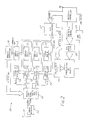
- FIG. 2 is a block diagram of a system 10 for displaying off-air video pictures on a bistable display, such as a ferroelectric liquid crystal display panel.
- Video information is received at aerial 11 and demodulated by the receiver 12; it is then digitized (four bits per pixel) and held in the digital frame store 13.
- the data For the sequential greyscale processing the data must be sent to the display one bit at a time, i.e. firstly all the data from RAM 0 is sent to the display (the least significant bit), then followed in turn by each of the other 3 RAMs. Also, in order to write data to the light crystal display panel each line of data mmust be presented in a manner determined by the multiplexing scheme; this processing is performed by the data preparation block 17. Data is now in a form in which it can be sent to the display panel under control of the multiplex controller block 18, each line of data being latched into the column drive chips 19 while rows are strobed by the low drive chips 20. This results in the data being latched into the display. After a full screen of data has been written, the backlight is flashed for a length of time corresponding to the significance of the bit being displayed. This is done by the lamp drive circuit 20 under control of the multiplex controller 18.
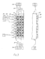
- Figure 3 shows an arrangement of metallisation patterns for a liquid crystal display panel to achiev a two-bit greyscale, for use additionally or alternatively to the greyscale processing of Figures 1 and 2.
- the ITO metallisation patterns are such that each pixel has two sections 31, 32 which can be separately driven from appropriate drive chips (not shown) on flexible pcb boards 33 and 34 via lines 35 and 36 respectively.
- section 31 corresponds to the least-significant-bit, and section 32 to the most-significant-bit.
- the row electrodes are formed by ITO metallisation strips 37 on substrate 38, which can be strobed by row drive chips (not shown) on flexible pcb 39 via lines 40.
- the substrate has been omitted as indicated by the broken-chain line yet the column metallisation is shown overlying the row metallisation, for the purpose of simplicity.
Abstract
Description
- The present invention relates to a display device, and particularly but not solely to one which utilizes liquid crystal display elements.
- A conventional liquid crystal display has a lattice of liquid crystal display elements each with its own driver and storage capacity to enable activation independently of the other elements. The on/off period of each element can be modulated in order to provide a number of intensity levels of display at that element.
- The present invention provides a display device to provide a grey-scale display, the device comprising:
a lattice of bi-stable display elements;
means to input a signal representing the display information for one picture to a store;
means to output, from the store, the display information for one picture in sections, each section consisting of corresponding portions of display information for all the bi-stable display elements;
a plurality of drivers, each allocated to a row or column of the lattice, to set each display element to a condition in accordance with its respective portion of the signal from the output means;
means to produce a light output; and
means to modulate the light output in accordance with the significance of the signal from the output means. - In this way, the display device does not require a driver for each element, thereby providing a substantial simplification in the arrangement of constituent components of the device, and enabling multiplexed operation of the display device.
- Preferably, the signal for one picture comprises a sequence of words (for example each of 8 bits), each one corresponding to the display information for a display element in the lattice. Thus the output means can operate such as to take out, from the store, the first bit in each word and pass them sequentially to the lattice; thereafter the output means can operate such as to take out, from the store, the second bit in each word and pass them sequentially to the lattice. This operation can be repeated until all the bits have been processed in this way.
- As the bits in a given position (e.g. first) in the display word reach the drivers, they set each pixel to the corresponding condition. Once the entire lattice has been set in accordance with a given bit-position, the light-modulation means can be activated to output light in accordance with the given bit-position; thus, for example, if the given bit-position is the first bit in the word and this is designated as the most-significant bit, when the light output with the elements in this condition is accordingly a substantial fraction of the total output. The light output for the most-significant-bit setting may be double that for the secondmost-significant-bit setting, which is itself double that for the third most-significant-bit setting, and so on. The light modulation means may have means to regulate the intensity of the light output in accordance witht he given bit-position, and/or means to regulate the duration of light output in accordance with the given bit-position.
- Preferably the display device may have means to blank the elements during setting of the elements for a given bit position.
- For a colour display, preferably the display device has a lattice formed of groups of three display elements, each of the elements in a group producing a different colour and being set separately. In an alternative arrangement, the lattice is formed of a single display elements, each of which is exposed to light of the three colours sequentially, an element being re-set after each exposure.
- The present invention also provides a method of operating a grey-scale display device having a lattice of bi-stable display elements, the method comprising:-
inputting a signal, representing the display information for one picture, to a store;
outputting from the store a section of the display information for one picture, the section consisting of corresponding portions of display information for all the bi-stable display elements;
using a plurality of drivers, each allocated to a row or column of the lattice, to effect setting of each display element to a condition in accordance with its respective portion of the signal from the output means;
producing a light output, one the elements are set, modulated in accordance with the significance of the portion of the video signal;
outputting from the store a second section of the display information, the second section consisting of different corresponding portions of display information for all the bi-stable display elements, and effecting the setting and modulating operations for the second section; and
repeating the outputting, setting and modulating operations on any further corresponding portions. - Preferably, the signal comprises an 8-bit word for each element, and the most-significant-bit of each word is first output from the store for setting and display. Thereafter the second-most-significant-bit of each word is output from the store for setting and display, the total light output being half the previous output. This sequence is repeated until the least-significant bit has been displayed.
- Preferably, modulation of the light output is achieved by regulation of the light intensity and/or of the duration of light output.
- Preferably, each row and column of the lattice has a separate driver. Alternatively, each column has a separate driver, and some or all the rows have a common driver.
- Preferably a display element comprises one or more selectively-settable liquid crystal cells.
- The present invention is applicable to many forms of displays, for example to one in which the image is presented at a surface of liquid crystal panel backlit by fluorescent tubes, or to one in which the image is projected onto a screen by means of a liquid crystal panel positioned in the path of a light beam. Also, the present invention is applicable to colour displays and to black-and-white displays.
- Furthermore, the present invention also embodies equipment for the generation, and/or transmission, and/or reception, and/or processing, of signals suited and/or designated for a display device as herein defined.
- In order that the invention may more readily be understood, a description is now given, by way of example only, reference being made to the sole accompanying drawings in which:
- Figure 1 is a block diagram of a display device embodying the present invention;
- Figure 2 is another block diagram of a display device embodying the present invention; and
- Figure 3 shows a pixel arrangement for a display device embodying the present invention.
- The
television receiver 1 of Figure 1 has aliquid crystal display 2 formed of a lattice ofdisplay elements 3 made from liquid crystal material, each element being individually actuable. The lattice ofelements 3 is backlit by a number of fluorescent tubes 4 whose light intensity and duration of operation can be controlled. - The video signal for input to television receiver has a 70Hz scan rate providing a scan period of 14mS, and includes in each picture of display information an 8-bit word for each display element, a word beginning with the most-significant-bit and ending with the least-significant-bit. When this signal is input to
receiver 1 via its aerial 5, one picture of display information passes to a frame store 6. - In the processing for the display of the most-significant- bits of the word, frame store 6 outputs the first bit of each word and sends the bits to a control unit 7 for an array of
drivers 8, one being assigned to each row and column of the lattice. The driver array sets each element to the condition (on or off) appropriate to its most-significant-bit. Once the array ofdrivers 8 has set all the elements (which takes less than 1mS), driver control unit 7 instructs light switch unit 9 which checks the relevant bit-position (in this case the most-significant-bit) and then activates the fluorescent tubes 4 for a time duration of 3mS and at an intensity to provide an appropriate output. - When the required output has been achieved then the light switch unit 9 de-activates the tubes 4 and instructs frame store 6 which proceeds to output the secondmost-significant bits to driver control unit 7 thereby to set all the elements for this bit-position. On this occasion, light switch unit 9 activates the tubes half as long as before (namely 1.5mS) at the same intensity to provide only half the output as that for the most-significant bits. This routine is repeated for all eight bits of the words, the light output being halved each time. Once the least significant bit has been displayed (the light output time duration being 25 S), the store 6 is emptied and the next picture of display information is output and the processing described above is repeated.
- Figure 2 is a block diagram of a
system 10 for displaying off-air video pictures on a bistable display, such as a ferroelectric liquid crystal display panel. Video information is received at aerial 11 and demodulated by thereceiver 12; it is then digitized (four bits per pixel) and held in thedigital frame store 13. - To display one video frame, firstly the data is split into four streams (one for each bit) and compressed by
shift registers 14 so each byte contains data for 8 pixels. The data is then loaded into fourbuffer RAMs 15, so each RAM now contains one frame ofvideo information 1 bit deep. Accessing of theRAMs 15 and the frame store is done under control of theaddress generator 16. - For the sequential greyscale processing the data must be sent to the display one bit at a time, i.e. firstly all the data from RAM 0 is sent to the display (the least significant bit), then followed in turn by each of the other 3 RAMs. Also, in order to write data to the light crystal display panel each line of data mmust be presented in a manner determined by the multiplexing scheme; this processing is performed by the
data preparation block 17. Data is now in a form in which it can be sent to the display panel under control of themultiplex controller block 18, each line of data being latched into thecolumn drive chips 19 while rows are strobed by thelow drive chips 20. This results in the data being latched into the display. After a full screen of data has been written, the backlight is flashed for a length of time corresponding to the significance of the bit being displayed. This is done by thelamp drive circuit 20 under control of themultiplex controller 18. - The sequence of events which results in a full picture with sixteen grey levels being displayed, is as follows:-
- 1.
Load frame store 13; - 2. Load buffer RAMs 15, one significant bit to each;
- 3. Load data from buffer RAM 0 line into
data preparation unit 17; - 4. Load data from
buffer RAM 1 line by line intodata preparation unit 17; - 5. Load data from
buffer RAM 2 line by line intodata preparation unit 17; - 6. Load data from
buffer RAM 3 line by line intodata preparation unit 17; - 7.
Multiplex controller 18 sends data frompreparation unit 17 to column drive chips 119 and controls row drive chips 20; - 8. When data from RAM 0 has been latched into the display (i.e. when the least significant bit for the frame is being presented), the
multiplex controller 18 signals the lamp drive to flash for a period of time A mS; - 9. Data from
RAM 1 is now latched and the backlight flashed for 2A mS; - 10. Data from
RAM 2 is now latched and the backlight flashed for 4A mS; - 11. Data from
RAM 3 is now latched and the backlight flashed for 8A mS; - 12. The picture has now been displayed.
- Figure 3 shows an arrangement of metallisation patterns for a liquid crystal display panel to achiev a two-bit greyscale, for use additionally or alternatively to the greyscale processing of Figures 1 and 2. On the
substrate 30 having the column electrodes, the ITO metallisation patterns are such that each pixel has twosections flexible pcb boards lines section 31 corresponds to the least-significant-bit, andsection 32 to the most-significant-bit. The row electrodes are formed by ITO metallisation strips 37 onsubstrate 38, which can be strobed by row drive chips (not shown) onflexible pcb 39 vialines 40. In Figure 3, on the left hand side the substrate has been omitted as indicated by the broken-chain line yet the column metallisation is shown overlying the row metallisation, for the purpose of simplicity.
Claims (11)
a lattice of bi-stable display elements;
means to input a signal representing the display information for one picture to a store;
means to output, from the store, the display information for one picture in sections, each section consisting of corresponding portions of display information for all the bi-stable display elements;
a plurality of drivers, each allocated to a row or column of the lattice, to set each display element to a condition in accordance with its respective portion of the signal from the output means;
means to produce a light output; and
means to modulate the light output in accordance with the significance of the signal from the output means.
inputting a signal, representing the display information for one picture, to a store;
outputting from the store a section of the display information for one picture, the section consisting of corresponding portions of display information for all the bi-stable display elements;
using a plurality of drivers, each allocated to a row or column of the lattice, to effect setting of each display element to a condition in accordance with its respective portion of the signal from the output means;
producing a light output, once the elements are set, modulated in accordance with the significance of the portion of the video signal;
outputting from the store a second section of the display information, the second section consisting of different corresponding portions of display information for all the bi-stable display elements, and effecting the setting and modulating operations for the second section; and
repeating the outputting, setting and modulating operations on any further corresponding portions.
Priority Applications (1)
| Application Number | Priority Date | Filing Date | Title |
|---|---|---|---|
| AT87308310T ATE79684T1 (en) | 1986-09-20 | 1987-09-18 | INDICATOR. |
Applications Claiming Priority (2)
| Application Number | Priority Date | Filing Date | Title |
|---|---|---|---|
| GB8622711 | 1986-09-20 | ||
| GB868622711A GB8622711D0 (en) | 1986-09-20 | 1986-09-20 | Display device |
Publications (3)
| Publication Number | Publication Date |
|---|---|
| EP0261897A2 true EP0261897A2 (en) | 1988-03-30 |
| EP0261897A3 EP0261897A3 (en) | 1989-01-18 |
| EP0261897B1 EP0261897B1 (en) | 1992-08-19 |
Family
ID=10604535
Family Applications (1)
| Application Number | Title | Priority Date | Filing Date |
|---|---|---|---|
| EP87308310A Expired - Lifetime EP0261897B1 (en) | 1986-09-20 | 1987-09-18 | Display device |
Country Status (8)
| Country | Link |
|---|---|
| EP (1) | EP0261897B1 (en) |
| JP (1) | JPS63278098A (en) |
| AT (1) | ATE79684T1 (en) |
| CA (1) | CA1295062C (en) |
| DE (1) | DE3781231T2 (en) |
| ES (1) | ES2033863T3 (en) |
| GB (1) | GB8622711D0 (en) |
| GR (1) | GR3005490T3 (en) |
Cited By (11)
| Publication number | Priority date | Publication date | Assignee | Title |
|---|---|---|---|---|
| EP0507270A1 (en) * | 1991-04-01 | 1992-10-07 | Texas Instruments Incorporated | DMD architecture and timing for use in a pulse-width modulated display system |
| GB2317290A (en) * | 1996-09-11 | 1998-03-18 | Seos Displays Ltd | Image display apparatus |
| US5903323A (en) * | 1994-12-21 | 1999-05-11 | Raytheon Company | Full color sequential image projection system incorporating time modulated illumination |
| US7653371B2 (en) | 2004-09-27 | 2010-01-26 | Qualcomm Mems Technologies, Inc. | Selectable capacitance circuit |
| US7808703B2 (en) | 2004-09-27 | 2010-10-05 | Qualcomm Mems Technologies, Inc. | System and method for implementation of interferometric modulator displays |
| US7903047B2 (en) | 2006-04-17 | 2011-03-08 | Qualcomm Mems Technologies, Inc. | Mode indicator for interferometric modulator displays |
| US7920135B2 (en) | 2004-09-27 | 2011-04-05 | Qualcomm Mems Technologies, Inc. | Method and system for driving a bi-stable display |
| US8059326B2 (en) | 1994-05-05 | 2011-11-15 | Qualcomm Mems Technologies Inc. | Display devices comprising of interferometric modulator and sensor |
| US8885244B2 (en) | 2004-09-27 | 2014-11-11 | Qualcomm Mems Technologies, Inc. | Display device |
| US8971675B2 (en) | 2006-01-13 | 2015-03-03 | Qualcomm Mems Technologies, Inc. | Interconnect structure for MEMS device |
| US9110289B2 (en) | 1998-04-08 | 2015-08-18 | Qualcomm Mems Technologies, Inc. | Device for modulating light with multiple electrodes |
Families Citing this family (1)
| Publication number | Priority date | Publication date | Assignee | Title |
|---|---|---|---|---|
| US8928967B2 (en) | 1998-04-08 | 2015-01-06 | Qualcomm Mems Technologies, Inc. | Method and device for modulating light |
Citations (5)
| Publication number | Priority date | Publication date | Assignee | Title |
|---|---|---|---|---|
| US4006298A (en) * | 1975-05-20 | 1977-02-01 | Gte Laboratories Incorporated | Bistable matrix television display system |
| US4378568A (en) * | 1981-01-29 | 1983-03-29 | Eastman Kodak Company | Light valve imaging apparatus and method for providing gray scale |
| US4559535A (en) * | 1982-07-12 | 1985-12-17 | Sigmatron Nova, Inc. | System for displaying information with multiple shades of a color on a thin-film EL matrix display panel |
| GB2164776A (en) * | 1984-08-18 | 1986-03-26 | Canon Kk | Matrix display devices |
| EP0193728A2 (en) * | 1985-03-08 | 1986-09-10 | Ascii Corporation | Display control system |
Family Cites Families (2)
| Publication number | Priority date | Publication date | Assignee | Title |
|---|---|---|---|---|
| JPS5968784A (en) * | 1982-10-13 | 1984-04-18 | シャープ株式会社 | Driver for dot matrix display panel |
| JPS6169036A (en) * | 1984-08-18 | 1986-04-09 | Canon Inc | Driving method of display panel |
-
1986
- 1986-09-20 GB GB868622711A patent/GB8622711D0/en active Pending
-
1987
- 1987-09-18 EP EP87308310A patent/EP0261897B1/en not_active Expired - Lifetime
- 1987-09-18 DE DE8787308310T patent/DE3781231T2/en not_active Expired - Fee Related
- 1987-09-18 AT AT87308310T patent/ATE79684T1/en not_active IP Right Cessation
- 1987-09-18 ES ES198787308310T patent/ES2033863T3/en not_active Expired - Lifetime
- 1987-09-21 CA CA000547373A patent/CA1295062C/en not_active Expired - Lifetime
- 1987-09-21 JP JP62235067A patent/JPS63278098A/en active Pending
-
1992
- 1992-08-20 GR GR920401830T patent/GR3005490T3/el unknown
Patent Citations (5)
| Publication number | Priority date | Publication date | Assignee | Title |
|---|---|---|---|---|
| US4006298A (en) * | 1975-05-20 | 1977-02-01 | Gte Laboratories Incorporated | Bistable matrix television display system |
| US4378568A (en) * | 1981-01-29 | 1983-03-29 | Eastman Kodak Company | Light valve imaging apparatus and method for providing gray scale |
| US4559535A (en) * | 1982-07-12 | 1985-12-17 | Sigmatron Nova, Inc. | System for displaying information with multiple shades of a color on a thin-film EL matrix display panel |
| GB2164776A (en) * | 1984-08-18 | 1986-03-26 | Canon Kk | Matrix display devices |
| EP0193728A2 (en) * | 1985-03-08 | 1986-09-10 | Ascii Corporation | Display control system |
Cited By (21)
| Publication number | Priority date | Publication date | Assignee | Title |
|---|---|---|---|---|
| KR100253106B1 (en) * | 1991-04-01 | 2000-05-01 | 윌리엄 비. 켐플러 | Dmd architecture and timing for use in a pulse-width modulated display system |
| US5278652A (en) * | 1991-04-01 | 1994-01-11 | Texas Instruments Incorporated | DMD architecture and timing for use in a pulse width modulated display system |
| EP0689344A2 (en) * | 1991-04-01 | 1995-12-27 | Texas Instruments Incorporated | DMD architecture and timing for use in a pulse-width modulated display system |
| EP0689343A2 (en) * | 1991-04-01 | 1995-12-27 | Texas Instruments Incorporated | DMD architecture and timing for use in a pulse-width modulated display system |
| EP0689344A3 (en) * | 1991-04-01 | 1996-05-15 | Texas Instruments Inc | DMD architecture and timing for use in a pulse-width modulated display system |
| EP0689343A3 (en) * | 1991-04-01 | 1996-05-15 | Texas Instruments Inc | DMD architecture and timing for use in a pulse-width modulated display system |
| US5523803A (en) * | 1991-04-01 | 1996-06-04 | Texas Instruments Incorporated | DMD architecture and timing for use in a pulse-width modulated display system |
| US5745193A (en) * | 1991-04-01 | 1998-04-28 | Texas Instruments Incorporated | DMD architecture and timing for use in a pulse-width modulated display system |
| EP0507270A1 (en) * | 1991-04-01 | 1992-10-07 | Texas Instruments Incorporated | DMD architecture and timing for use in a pulse-width modulated display system |
| US8059326B2 (en) | 1994-05-05 | 2011-11-15 | Qualcomm Mems Technologies Inc. | Display devices comprising of interferometric modulator and sensor |
| US5903323A (en) * | 1994-12-21 | 1999-05-11 | Raytheon Company | Full color sequential image projection system incorporating time modulated illumination |
| US5978142A (en) * | 1996-09-11 | 1999-11-02 | Seos Display, Limited | Image display apparatus with modulators for modulating picture elements in an image |
| GB2317290B (en) * | 1996-09-11 | 2000-12-06 | Seos Displays Ltd | Image display apparatus |
| GB2317290A (en) * | 1996-09-11 | 1998-03-18 | Seos Displays Ltd | Image display apparatus |
| US9110289B2 (en) | 1998-04-08 | 2015-08-18 | Qualcomm Mems Technologies, Inc. | Device for modulating light with multiple electrodes |
| US7653371B2 (en) | 2004-09-27 | 2010-01-26 | Qualcomm Mems Technologies, Inc. | Selectable capacitance circuit |
| US7808703B2 (en) | 2004-09-27 | 2010-10-05 | Qualcomm Mems Technologies, Inc. | System and method for implementation of interferometric modulator displays |
| US7920135B2 (en) | 2004-09-27 | 2011-04-05 | Qualcomm Mems Technologies, Inc. | Method and system for driving a bi-stable display |
| US8885244B2 (en) | 2004-09-27 | 2014-11-11 | Qualcomm Mems Technologies, Inc. | Display device |
| US8971675B2 (en) | 2006-01-13 | 2015-03-03 | Qualcomm Mems Technologies, Inc. | Interconnect structure for MEMS device |
| US7903047B2 (en) | 2006-04-17 | 2011-03-08 | Qualcomm Mems Technologies, Inc. | Mode indicator for interferometric modulator displays |
Also Published As
| Publication number | Publication date |
|---|---|
| DE3781231D1 (en) | 1992-09-24 |
| ATE79684T1 (en) | 1992-09-15 |
| EP0261897B1 (en) | 1992-08-19 |
| GB8622711D0 (en) | 1986-10-29 |
| CA1295062C (en) | 1992-01-28 |
| ES2033863T3 (en) | 1993-04-01 |
| GR3005490T3 (en) | 1993-05-24 |
| JPS63278098A (en) | 1988-11-15 |
| EP0261897A3 (en) | 1989-01-18 |
| DE3781231T2 (en) | 1993-03-11 |
Similar Documents
| Publication | Publication Date | Title |
|---|---|---|
| EP0261896B1 (en) | Display device | |
| US5093652A (en) | Display device | |
| CN101231823B (en) | Display device and electronic equipment comprising the same | |
| KR100274838B1 (en) | A method and system controller for spatial light modulator display | |
| US5912651A (en) | Matrix display systems and methods of operating such systems | |
| US4833464A (en) | Electrophoretic information display (EPID) apparatus employing grey scale capability | |
| US4921334A (en) | Matrix liquid crystal display with extended gray scale | |
| DE69731724T2 (en) | Integrated circuit for controlling a pixel-inversion liquid crystal display device | |
| EP0261901B1 (en) | Display device | |
| JP3266288B2 (en) | Display device and operation method thereof | |
| US4901155A (en) | Signal processing system for large screen display apparatus | |
| EP0261897B1 (en) | Display device | |
| EP0261898A2 (en) | Display device | |
| DE69737946T2 (en) | Method for driving an AC plasma display panel | |
| US3838209A (en) | Scanning apparatus for a matrix display panel | |
| JP2612475B2 (en) | Display control device for color display panel | |
| CA2161184A1 (en) | Panel type color display device and system for processing image information | |
| KR950006520A (en) | Image display device and driving method thereof | |
| CA2223371A1 (en) | Frame display control in an image display having a liquid crystal display panel | |
| US11132844B2 (en) | Driving method and driving apparatus for AR/VR display device, and display device | |
| CA2164803C (en) | Method and circuit for driving picture display devices | |
| WO1999050817A1 (en) | Blacklight control for a display device | |
| KR100256841B1 (en) | Process and device for driving matrix display | |
| JPH06266310A (en) | Liquid crystal display device | |
| KR0118493Y1 (en) | The data separation driving system of a plasma display panel |
Legal Events
| Date | Code | Title | Description |
|---|---|---|---|
| PUAI | Public reference made under article 153(3) epc to a published international application that has entered the european phase |
Free format text: ORIGINAL CODE: 0009012 |
|
| AK | Designated contracting states |
Kind code of ref document: A2 Designated state(s): AT BE CH DE ES FR GB GR IT LI LU NL SE |
|
| PUAL | Search report despatched |
Free format text: ORIGINAL CODE: 0009013 |
|
| AK | Designated contracting states |
Kind code of ref document: A3 Designated state(s): AT BE CH DE ES FR GB GR IT LI LU NL SE |
|
| 17P | Request for examination filed |
Effective date: 19890213 |
|
| 17Q | First examination report despatched |
Effective date: 19910319 |
|
| GRAA | (expected) grant |
Free format text: ORIGINAL CODE: 0009210 |
|
| ITF | It: translation for a ep patent filed |
Owner name: FUMERO BREVETTI S.N.C. |
|
| AK | Designated contracting states |
Kind code of ref document: B1 Designated state(s): AT BE CH DE ES FR GB GR IT LI LU NL SE |
|
| REF | Corresponds to: |
Ref document number: 79684 Country of ref document: AT Date of ref document: 19920915 Kind code of ref document: T |
|
| REF | Corresponds to: |
Ref document number: 3781231 Country of ref document: DE Date of ref document: 19920924 |
|
| ET | Fr: translation filed | ||
| REG | Reference to a national code |
Ref country code: GR Ref legal event code: FG4A Free format text: 3005490 |
|
| REG | Reference to a national code |
Ref country code: ES Ref legal event code: FG2A Ref document number: 2033863 Country of ref document: ES Kind code of ref document: T3 |
|
| PLBE | No opposition filed within time limit |
Free format text: ORIGINAL CODE: 0009261 |
|
| STAA | Information on the status of an ep patent application or granted ep patent |
Free format text: STATUS: NO OPPOSITION FILED WITHIN TIME LIMIT |
|
| PGFP | Annual fee paid to national office [announced via postgrant information from national office to epo] |
Ref country code: SE Payment date: 19930721 Year of fee payment: 7 Ref country code: CH Payment date: 19930721 Year of fee payment: 7 |
|
| PGFP | Annual fee paid to national office [announced via postgrant information from national office to epo] |
Ref country code: AT Payment date: 19930722 Year of fee payment: 7 |
|
| PGFP | Annual fee paid to national office [announced via postgrant information from national office to epo] |
Ref country code: GR Payment date: 19930728 Year of fee payment: 7 |
|
| 26N | No opposition filed | ||
| PGFP | Annual fee paid to national office [announced via postgrant information from national office to epo] |
Ref country code: ES Payment date: 19930811 Year of fee payment: 7 |
|
| PGFP | Annual fee paid to national office [announced via postgrant information from national office to epo] |
Ref country code: LU Payment date: 19930908 Year of fee payment: 7 |
|
| PGFP | Annual fee paid to national office [announced via postgrant information from national office to epo] |
Ref country code: BE Payment date: 19930915 Year of fee payment: 7 |
|
| EPTA | Lu: last paid annual fee | ||
| PGFP | Annual fee paid to national office [announced via postgrant information from national office to epo] |
Ref country code: GB Payment date: 19940727 Year of fee payment: 8 |
|
| PGFP | Annual fee paid to national office [announced via postgrant information from national office to epo] |
Ref country code: FR Payment date: 19940728 Year of fee payment: 8 |
|
| PG25 | Lapsed in a contracting state [announced via postgrant information from national office to epo] |
Ref country code: LU Free format text: LAPSE BECAUSE OF NON-PAYMENT OF DUE FEES Effective date: 19940918 Ref country code: AT Effective date: 19940918 |
|
| PG25 | Lapsed in a contracting state [announced via postgrant information from national office to epo] |
Ref country code: SE Effective date: 19940919 Ref country code: ES Free format text: LAPSE BECAUSE OF THE APPLICANT RENOUNCES Effective date: 19940919 |
|
| PG25 | Lapsed in a contracting state [announced via postgrant information from national office to epo] |
Ref country code: LI Effective date: 19940930 Ref country code: CH Effective date: 19940930 Ref country code: BE Effective date: 19940930 |
|
| PGFP | Annual fee paid to national office [announced via postgrant information from national office to epo] |
Ref country code: NL Payment date: 19940930 Year of fee payment: 8 |
|
| PGFP | Annual fee paid to national office [announced via postgrant information from national office to epo] |
Ref country code: DE Payment date: 19941125 Year of fee payment: 8 |
|
| EAL | Se: european patent in force in sweden |
Ref document number: 87308310.9 |
|
| BERE | Be: lapsed |
Owner name: THORN EMI P.L.C. Effective date: 19940930 |
|
| PG25 | Lapsed in a contracting state [announced via postgrant information from national office to epo] |
Ref country code: GR Free format text: THE PATENT HAS BEEN ANNULLED BY A DECISION OF A NATIONAL AUTHORITY Effective date: 19950331 |
|
| REG | Reference to a national code |
Ref country code: CH Ref legal event code: PL Ref country code: GR Ref legal event code: MM2A Free format text: 3005490 |
|
| EUG | Se: european patent has lapsed |
Ref document number: 87308310.9 |
|
| PG25 | Lapsed in a contracting state [announced via postgrant information from national office to epo] |
Ref country code: GB Effective date: 19950918 |
|
| PG25 | Lapsed in a contracting state [announced via postgrant information from national office to epo] |
Ref country code: NL Effective date: 19960401 |
|
| GBPC | Gb: european patent ceased through non-payment of renewal fee |
Effective date: 19950918 |
|
| PG25 | Lapsed in a contracting state [announced via postgrant information from national office to epo] |
Ref country code: FR Effective date: 19960531 |
|
| PG25 | Lapsed in a contracting state [announced via postgrant information from national office to epo] |
Ref country code: DE Effective date: 19960601 |
|
| NLV4 | Nl: lapsed or anulled due to non-payment of the annual fee |
Effective date: 19960401 |
|
| REG | Reference to a national code |
Ref country code: FR Ref legal event code: ST |
|
| REG | Reference to a national code |
Ref country code: ES Ref legal event code: FD2A Effective date: 19991007 |
|
| PG25 | Lapsed in a contracting state [announced via postgrant information from national office to epo] |
Ref country code: IT Free format text: LAPSE BECAUSE OF NON-PAYMENT OF DUE FEES Effective date: 20050918 |