EP0266016A2 - Automatic circuit board configuration - Google Patents
Automatic circuit board configuration Download PDFInfo
- Publication number
- EP0266016A2 EP0266016A2 EP87304207A EP87304207A EP0266016A2 EP 0266016 A2 EP0266016 A2 EP 0266016A2 EP 87304207 A EP87304207 A EP 87304207A EP 87304207 A EP87304207 A EP 87304207A EP 0266016 A2 EP0266016 A2 EP 0266016A2
- Authority
- EP
- European Patent Office
- Prior art keywords
- circuit board
- counter
- board
- address
- clock
- Prior art date
- Legal status (The legal status is an assumption and is not a legal conclusion. Google has not performed a legal analysis and makes no representation as to the accuracy of the status listed.)
- Withdrawn
Links
- 230000006870 function Effects 0.000 claims description 17
- 239000004020 conductor Substances 0.000 description 11
- 239000000872 buffer Substances 0.000 description 10
- 238000010586 diagram Methods 0.000 description 4
- 238000001485 positron annihilation lifetime spectroscopy Methods 0.000 description 4
- 230000001360 synchronised effect Effects 0.000 description 4
- 238000009434 installation Methods 0.000 description 1
- 238000012986 modification Methods 0.000 description 1
- 230000004048 modification Effects 0.000 description 1
- 230000004044 response Effects 0.000 description 1
Images

Classifications
-
- G—PHYSICS
- G06—COMPUTING; CALCULATING OR COUNTING
- G06F—ELECTRIC DIGITAL DATA PROCESSING
- G06F12/00—Accessing, addressing or allocating within memory systems or architectures
- G06F12/02—Addressing or allocation; Relocation
- G06F12/06—Addressing a physical block of locations, e.g. base addressing, module addressing, memory dedication
- G06F12/0646—Configuration or reconfiguration
- G06F12/0669—Configuration or reconfiguration with decentralised address assignment
- G06F12/0676—Configuration or reconfiguration with decentralised address assignment the address being position dependent
Definitions
- FIGURE 1 illustrates a system including a series of circuit boards such as a first circuit board 12, a second circuit board 14, a third circuit board 16 and additional circuit boards up to the Nth circuit board.
- Each circuit board has a Programmable Array Logic (PAL) integrated circuit thereon, and is shown at 18, 20 and 22 on the first, second and third circuit boards 12, 14 and 16, respectively.
- PAL Programmable Array Logic
- Each of these circuit boards also has memory means such as an Erasable Programmable Read Only Memory (EPROM) thereon and is shown at 24, 26 and 28 on the first, second and third circuit boards 12, 14 and 16, respectively.
- EPROM Erasable Programmable Read Only Memory
- PROM Programmable Read Only Memory
- ROM Read Only Memory
- EPROMS 24, 26 and 28 are connected to the system backplane through conductors 30, 32 and 34, respectively.
- the first four slots of the backplane are reserved for processor boards, although it is not necessary for a processor board to be plugged into the second, third or fourth slots if only one processor board is needed for the task or tasks being performed.
- a processor board need only be plugged into the first slot or the "0" address slot.
- the remainder of the slots may be occupied by other boards, for example, input-output circuit boards.
- the processor board which is in the first or "0" address slot is considered to be the processor board with the highest priority when multiple processors are installed.
- the system controller board 47 includes a RAM into which the address and corresponding identifier codes are to be read and a program which accomplishes this task.
Abstract
An apparatus for automatically providing an indication of the operable position of a circuit board plugged into the back plane of a device. The apparatus also automatically provides an indication as to the capabilities of each specific circuit board and to associate the capabilities with the specific location.
Description
- The present invention generally relates to devices utilizing circuit boards and, more particularly, is concerned with allowing any particular circuit board to be plugged into any backplane slot of the device.
- In most devices which utilize circuit boards, the device includes a backplane having a plurality of slots which receive circuit boards and each slot is preassigned a separate fixed address. For example, a plurality of wires (usually 4 or 5) are physically connected to each slot. These wires determine the maximum number of circuit boards which can be inserted into the backplane. For example, if 4 wires were utilized, the maximum number of circuit boards would be 16, and if 5 wires were utilized, the maximum number of circuit boards would be 32. Each wire represents a binary digit, therefore, each slot is assigned an address and that address is fixed to that one particular slot and thus to any circuit board plugged into that slot..
- Each circuit board performs a particular function and it is required that each circuit board is assigned to a predetermined slot (address) which it must occupy for the device to function properly. For example, a circuit board which performs function A is required to be placed in the slot having an address A1, and a circuit board which performs function B is required to be placed in the slot having the address B1. If a slot is not required to have a circuit board plugged into it, a jumper board may be required to insure that the data is transferred from one place to another. Since each of the circuit boards is required to be plugged into a predetermined slot, an inventory or record of what circuit board must be plugged into what slot must be maintained and utilized each time the device is reconfigured to perform different tasks.
- Alternatively, in another implementation, each circuit board is preassigned a fixed address wherein the backplane slots are identical, that is, the boards are assigned the function of decoding their particular address rather than the backplane slots themselves having unique identifying addresses. In this case, care must be taken to avoid overlapping assigned addresses, all of which must be manually installed.
- Anyone who works with the circuit boards in a device must know exactly which board is to be placed in which slot. By requiring a person to plug a certain circuit board into a certain slot, time is wasted and mistakes are easily made. Alternatively, the person must endure substantial effort in appropriately configuring various circuit boards for differing applications, undoubtedly an error prone task. The inventory or record may be lost or destroyed which may render the device inoperative since the device will not operate if a circuit board is misplaced or circuit boards may be damaged due to improper installation.
- The present invention resides in a system operating within a device whereby a series of circuit boards may be randomly plugged into the device. The system includes a backplane having slots for receiving the circuit boards. Each circuit board performs one or more operations and includes a memory device for storing an identifier code which represents the capabilities of the specific circuit board. Each circuit board also includes means for generating an address code which represents the specific logical location of that circuit board on the backplane. The system also includes a means for reading each of the address codes and the identifier codes associated therewith thereby identifying the location and operation configuration of each circuit board for use in processing of data received by the system.
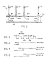
- In the drawings:
- FIGURE 1 shows the present invention as applied to three circuit boards;
- FIGURE 2 is a top view of the circuit boards plugged into the backplane slots;
- FIGURE 3 is a timing diagram of a clock signal applied to the system shown in FIGURE 1;
- FIGURE 4 is a timing diagram of a reset signal applied to the system shown in FIGURE 1;
- FIGURE 5 is a diagram of a waveform generated by the first circuit board and received by the input gate of the second circuit board;
- FIGURE 6 is a diagram of a waveform generated by the second circuit board and received by the input gate of the third circuit board.
- In accordance with the principles of the present invention there is provided means whereby the user of a data processing system may utilize various available circuit boards to perform desired known functions without concern for where those circuit boards are inserted into the system. For example, the user may require four processor boards and twelve input/output (I/O) boards having known functions to perform processing of data to be received. These boards may be arbitrarily inserted into the board receiving slots by the user after which, upon being activated, the user and the system will be automatically provided with required information as to the specific address of each of the boards and the function or functions which each of the boards is capable of performing. Thereafter the system controller can automatically communicate with the data to the desired board for appropriate processing of data. The automatic provision of the information illustrative of the specific configuration of the boards (the auto-configuration function) is accomplished using only the standard clock signal and the standard reset signal of the system and by inerconnecting the boards in a daisy chain fashion.
- In a system using the present invention each of the circuit boards has a programmable read only memory (PROM) which stores an identifier code representing the particular operation or operations which the circuit board is capable of performing. When the system is turned on, the identifier code stored in the memory, as well as the specific address generated for the slot in which the circuit board is inserted, are provided to the system controller. By thus having the specific operations which can be performed at specific addresses on the backplane, the system controller is then capable of transferring data from one particular area of the system to another in accordance with the desired application.
- FIGURE 1 illustrates a system including a series of circuit boards such as a
first circuit board 12, asecond circuit board 14, a third circuit board 16 and additional circuit boards up to the Nth circuit board. Each circuit board has a Programmable Array Logic (PAL) integrated circuit thereon, and is shown at 18, 20 and 22 on the first, second andthird circuit boards third circuit boards conductors 30, 32 and 34, respectively. - Generally, a circuit board is capable of performing one or more specific operations such as fix gain, fix offset, scale, compute phase and the like. In the present invention, each of the boards and its operations is represented by a code. The identifier code stored in the EPROM of each circuit board is read by the
system controller 47 of FIGURE 2 and is input into a "look-up" table resident in the system controller memory. The "look-up" table subsequently contains an inventory of all of the identifier codes and the operation which each code represents. Thus, by utilizing identifier codes stored in an EPROM on each circuit board, information regarding the circuit board′s operation and associated logical address is readily available to the system controller. -
First circuit board 12 also includesbuffer 36,second circuit board 14 also includesbuffer 38, and third circuit board 16 also includes buffer 40. A clock signal is applied from a system clock source 42 to asignal bus 44 which in turn is connected throughconductors buffers reset signal source 52 to a secondsubnal bus 54 which in turn is connected throughconductors buffers buffers buffers PAL 18 throughconductor 62,PAL 20 throughconductor 64 andPAL 22 throughconductor 66, respectively. The synchronized reset signal frombuffer 36, is applied toPAL 18 throughconductor 68, the synchornized reset signal frombuffer 38 is applied toPAL 20 through conductor 70 and the system reset signal from buffer 40 is applied toPAL 22 throughconductor 72. - The
PALS counter first slot 39. Assumingcircuit board 12 is in the first slot,input gate 76 of thesecond circuit board 14 is connected toPAL 18 on thefirst circuit board 12. Additionally,input gate 78 on the third circuit board 16 is connected to thePAL 20 on thesecond circuit board 14. Theinput gate 74 on thefirst circuit board 12 is connected to a constant high or binary one signal as represented by the pull-up resistor 81 thereby disabling the counter inPAL 18 from incrementing above a rest value of binary "00000". - Referring to the top view shown in FIGURE 2, the circuit boards are plugged into slots in a backplane as shown by the arrow 37. The backplane includes a separate slot for receiving each of the circuit boards, for example,
slot 39 receivesfirst circuit board 12,slot 41 receivessecond circuit board 14slot 43 receives third circuit board 16 andslot 45 receives circuit board N. Thesystem controller 47 which receives information regarding the location and function of each circuit board, is coupled to thebackplane 35 as illustrated by thedashed lines 46. - The count of each counter 73, 75 and 77 representing the uniquely determined identifying address code of each board is output through five board address lines at 84, 86 and 88, respectively. Referring to FIGURES 3 through 6, the operation of the system is illustrated. FIGURE 3 shows the system clock signal applied to each of the
PALS conductors PALS conductors counters first input gate 74, receive a low signal thereby enabling the counters to increment. Since thefirst input gate 74 is biased to a high signal, the counter in thefirst PAL 18 is disabled and will not increment but each remaining counter in the daisy-chain will increment. - Each bord in the daisy-chain will increment one count for each clock cycle such as 92 providing its corresponding input enable
signal clock cycle 92 later, it also outputs an inhibit command which disables further counting by the receiving board its successor in the daisy-chain. The final counter readout is then the address for that particular board. - The first clock cycle after the system is turned on is shown as 101 in FIGURE 3. During clock cycle 101, all of the counters are at decimal "0". Since the
first input gate 74 has a high signal connected to it at the beginning of thesecond clock cycle 92, counter 73 in thefirst PAL 18 will not increment and thefirst PAL 18 will output a high signal at the end of theclock signal 92 which is the count enable input toPAL 20. The end of this clock signal is shown aspoint 94 in FIGURE 3. After completion of thesecond clock cycle 92, counter 73 in thefirst PAL 18 is at "0" while thecounters 75 and 77 inPALS second input gate 76 is shown in FIGURE 5 and illustrates that the waveform changes from low to high as shown at 96 when the clock signal reachespoint 94. Thus, counter 75 in thesecond PAL 20 is disabled from further incrementing for the next clock cycle active edge 96 thereby preventing it from incrementing any further than "1". During the next clock cycle 102, counter 73 in thefirst PAL 18 is at "0", counter 75 in thesecond PAL 20 is at "1" and counter 77 in thethird PAL 22 is at "1". The output from thesecond PAL 20 changes from a low to a high signal at the end of clock cycle 102 which is shown at 98 in FIGURE 3. Therefore, thethird input gate 78 receives a waveform as shown in FIGURE 6 whereby atpoint 98 the waveform changes from low to high as shown at 100 and counter 77 inPAL 22 increments to "2". The waveform in FIGURE 6 disables. counter 77 in thethird PAL 22 during the next clock cycle 103, thereby preventing it from incrementing further. As this daisy chain type of reaction occurs, each of the additional counters will sequentially increment further until inhibited by its predecessor board. Thus, at the board address lines 84, 86 and 88, the address for each of the circuit boards corresponding to its position in the daisy-chain is established. If the clock signal frequency is at 16 MHz, it would take approximately 1 microsecond to establish addresses for sixteen circuit boards. - If a slot does not have a circuit board plugged into it, then a jumper is inserted into that slot if there are boards in subsequent slots. For example, if the slot between
circuit boards 12 and 16 was not occupied bycircuit board 14, a jumper would be used to connect the output of thefirst PAL 18 as shown at 80 to theinput gate 78 of thethird PAL 22. Therefore, the second slot would not have a board with a readable address associated with it. The board address line 84 of thefirst circuit board 12 would output "0" and the board address line 88 of the circuit board 16 would output "1". Jumpers are only necessary when a slot is skipped and then circuit boards are inserted into subsequent slots. If consecutive slots are filled starting from the first slot, then it is not necessary to use jumpers. For example, if there are sixteen slots available and the first six slots are filled by circuit boards, then the last ten slots need not have jumpers inserted into them. - In the preferred embodiment, the first four slots of the backplane are reserved for processor boards, although it is not necessary for a processor board to be plugged into the second, third or fourth slots if only one processor board is needed for the task or tasks being performed. For this particular case, a processor board need only be plugged into the first slot or the "0" address slot. The remainder of the slots may be occupied by other boards, for example, input-output circuit boards. The processor board which is in the first or "0" address slot is considered to be the processor board with the highest priority when multiple processors are installed. The
system controller board 47 includes a RAM into which the address and corresponding identifier codes are to be read and a program which accomplishes this task. Once the RAM on the system controller board has accumulated all the addresses (position information) and corresponding identifier codes (operational information), the information is then provided by the system controller to a computer memory through a general purpose interface bus (GPIB) for further use in processing the data and to processors installed within the system itself for local purposes. - Alternatively, the highest priority processor board can be assigned the task of acquiring the address and identifier codes in the absence of a system controler board providing that function.
- From the foregoing, it has been shown that the present invention provides a system which allows any circuit board to be plugged into any backplane slot. Information regarding the functional capability of each circuit board, along with the location of each circuit board, is available without the necessity of using jumpers, cables, or utilization of any other manual or similar operation. Although a specific embodiment has been illustrated and described, various modifications and changes may be made without departing from the spirit and scope of the invention.
Claims (8)
1. A system operating within a device whereby a plurality of circuit boards are plugged randomly into the device and the specific function or functions of each board as well as its location are automatically provided for data processing, the system comprising:
(A) a backplane for receiving the circuit boards, said backplane having a slot for each circuit board;
(B) each circuit board having one or more functions and including
-1- a memory device for storing an identifier code which represents the circuit board′s particular function, and
-2- means for generating an address code which represents the location of the circuit board on the backplane; and
(C) means for reading and each said identifier code thereby identifying the location and function of each circuit board.
2. The system as defined in claim 1 further comprising a system controller, means for providing said identifier codes and position address codes to said controller, whereby said location and operation information of each circuit board is used for transfer of data in accordance with the specific location and operation of each circuit board.
3. The system as defined in claim 2 wherein said reading means comprises a system controller circuit board which is plugged into a backplane, the system controller circuit board including a Programmable Read Only Memory (PROM) and a Random Access Memorum (RAM), means commanding said identifier codes and address of each board be recorded in a Random Access Memory (RAM) system controler circuit board.
4. The system as defined in claim 2 wherein said reading means comprises a first processor circuit board which is plugged into a first predetermined backplane slot having a predetermined first priority, the processor circuit board including a first Programmable Read Only Memory (PROM), Random Access Memory (RAM) means commanding said identifier codes and address of each board be recorded in said RAM on said first processor circuit board.
5. The system as defined in claim 3 wherein each circuit board in the daisy-chain is assigned a unique address and said address code generating means further comprises:
a Programmable Array Logic (PAL) which includes a counter means having an input clock enable and clock gate;
a clock signal generator means connected to input gate of each counter means;
a system reset signal generator means connected to a clock enable input gate of each counter means;
means for terminating counter incrementation upon receipt of the negation of the clock eanble signal and upon coincidence thereof to produce an inhibit signal; and
means for applying said inhibit signal to the input gate of the counter in the circuit board located in the slot in the next successive position in the daisy-chain.
6. The system as defined in claim 4 wherein each circuit board in the daisy-chain is assigned a unique address and said address code generating means further comprises:
a Programmable Array Logic (PAL) which includes a counter means having an input clock enable and clock gate;
a clock signal generator means connected to input gate of each counter means;
a system reset signal generator means connected to a clock enable input gate of each counter means;
means for terminating counter incrementation upon receipt of the negation of the clock eanble signal and upon coincidence thereof to produce an inhibit signal; and
means for applying said inhibit signal to the input gate of the counter in the circuit board located in the slot in the next successive position in the daisy-chain.
7. The system as defined in claim 5 wherein said system further includes a General Purpose Interface Bus (GPIB) and wherein said system controller board provides through said GPIB location and operational information of each circuit board to a computer means where it is stored for further use in data processing.
8. The system as defined in claim 6 wherein said system further includes a General Purpose Interface Bus (GPIB) and wherein said board of said first priority provides through said GPIB location and operational information of each circuit board to a computer means where it is stored for further use in data processing.
Applications Claiming Priority (2)
| Application Number | Priority Date | Filing Date | Title |
|---|---|---|---|
| US92423586A | 1986-10-28 | 1986-10-28 | |
| US924235 | 1986-10-28 |
Publications (1)
| Publication Number | Publication Date |
|---|---|
| EP0266016A2 true EP0266016A2 (en) | 1988-05-04 |
Family
ID=25449931
Family Applications (1)
| Application Number | Title | Priority Date | Filing Date |
|---|---|---|---|
| EP87304207A Withdrawn EP0266016A2 (en) | 1986-10-28 | 1987-05-12 | Automatic circuit board configuration |
Country Status (3)
| Country | Link |
|---|---|
| EP (1) | EP0266016A2 (en) |
| JP (1) | JPS63115259A (en) |
| IL (1) | IL82529A0 (en) |
Cited By (5)
| Publication number | Priority date | Publication date | Assignee | Title |
|---|---|---|---|---|
| DE4027202A1 (en) * | 1989-10-18 | 1991-04-25 | Siemens Ag | Processor system with processor and memory control unit - has identification memories associated with memory modules, facilitates changing module capacities |
| EP0546401A1 (en) * | 1991-12-10 | 1993-06-16 | Cerberus Ag | Addressing method for anti-theft, for fire and for gas alarm |
| WO1998003921A1 (en) * | 1996-07-23 | 1998-01-29 | 3Com Ireland | Cascade connection of communicating devices |
| EP0849684A2 (en) * | 1996-12-18 | 1998-06-24 | Sun Microsystems, Inc. | Computer bus expansion |
| EP1179784A1 (en) * | 2000-08-11 | 2002-02-13 | Siemens Aktiengesellschaft | Automation device |
-
1987
- 1987-05-12 EP EP87304207A patent/EP0266016A2/en not_active Withdrawn
- 1987-05-14 IL IL82529A patent/IL82529A0/en unknown
- 1987-05-20 JP JP62121436A patent/JPS63115259A/en active Pending
Cited By (11)
| Publication number | Priority date | Publication date | Assignee | Title |
|---|---|---|---|---|
| DE4027202A1 (en) * | 1989-10-18 | 1991-04-25 | Siemens Ag | Processor system with processor and memory control unit - has identification memories associated with memory modules, facilitates changing module capacities |
| EP0546401A1 (en) * | 1991-12-10 | 1993-06-16 | Cerberus Ag | Addressing method for anti-theft, for fire and for gas alarm |
| WO1998003921A1 (en) * | 1996-07-23 | 1998-01-29 | 3Com Ireland | Cascade connection of communicating devices |
| GB2331435A (en) * | 1996-07-23 | 1999-05-19 | 3Com Ireland | Casdade connection of communicating devices |
| EP1008943A2 (en) * | 1996-07-23 | 2000-06-14 | 3Com Ireland | Cascade connection of communicating devices |
| EP1008943A3 (en) * | 1996-07-23 | 2001-10-31 | 3COM Technologies | Cascade connection of communicating devices |
| US6523070B1 (en) * | 1996-07-23 | 2003-02-18 | 3Com Corporation | Communication device with circuitry to promote cascade series connection including identification of device position in the series and sensing the end device in the series |
| EP0849684A2 (en) * | 1996-12-18 | 1998-06-24 | Sun Microsystems, Inc. | Computer bus expansion |
| EP0849684A3 (en) * | 1996-12-18 | 1998-07-22 | Sun Microsystems, Inc. | Computer bus expansion |
| US5974489A (en) * | 1996-12-18 | 1999-10-26 | Sun Micro Systems | Computer bus expansion |
| EP1179784A1 (en) * | 2000-08-11 | 2002-02-13 | Siemens Aktiengesellschaft | Automation device |
Also Published As
| Publication number | Publication date |
|---|---|
| IL82529A0 (en) | 1987-11-30 |
| JPS63115259A (en) | 1988-05-19 |
Similar Documents
| Publication | Publication Date | Title |
|---|---|---|
| US4964038A (en) | Data processing system having automatic address allocation arrangements for addressing interface cards | |
| US4320467A (en) | Method and apparatus of bus arbitration using comparison of composite signals with device signals to determine device priority | |
| US3470542A (en) | Modular system design | |
| US4034347A (en) | Method and apparatus for controlling a multiprocessor system | |
| US4313160A (en) | Distributed input/output controller system | |
| US3766526A (en) | Multi-microprogrammed input-output processor | |
| US4630041A (en) | Enhanced reliability interrupt control apparatus | |
| CA1179409A (en) | Communication multiplexer having a variable priority scheme using a read only memory | |
| US4257097A (en) | Multiprocessor system with demand assignable program paging stores | |
| US3229259A (en) | Multiple rate data system | |
| GB1560164A (en) | Data processing system | |
| US3833930A (en) | Input/output system for a microprogram digital computer | |
| EP0010191A1 (en) | Data processing apparatus including an I/O monitor circuit | |
| EP0321628A1 (en) | Shared memory interface for a data processing system | |
| US3801962A (en) | Communication mechanism for data transfer and control between data processing systems and subsystems | |
| JPS6035697B2 (en) | input/output control system | |
| US4670855A (en) | Interchangeable interface circuit structure | |
| US4380065A (en) | Communication multiplexer variable priority scheme | |
| EP0266016A2 (en) | Automatic circuit board configuration | |
| EP0265575B1 (en) | Data processing system having automatic address allocation arrangements for addressing interface cards | |
| US4791553A (en) | Control unit of input-output interface circuits in an electronic processor | |
| US3858187A (en) | Read only memory system | |
| GB2060961A (en) | Data processing system having memory modules with distributed address information | |
| EP0087368B1 (en) | Interchangeable interface circuit structure | |
| US4198682A (en) | Symptom compression device |
Legal Events
| Date | Code | Title | Description |
|---|---|---|---|
| PUAI | Public reference made under article 153(3) epc to a published international application that has entered the european phase |
Free format text: ORIGINAL CODE: 0009012 |
|
| AK | Designated contracting states |
Kind code of ref document: A2 Designated state(s): DE FR GB IT |
|
| STAA | Information on the status of an ep patent application or granted ep patent |
Free format text: STATUS: THE APPLICATION IS DEEMED TO BE WITHDRAWN |
|
| 18D | Application deemed to be withdrawn |
Effective date: 19890601 |
|
| RIN1 | Information on inventor provided before grant (corrected) |
Inventor name: LEVASSEUR, DAN |