EP0267513A2 - Microwave enhanced CVD method and apparatus - Google Patents
Microwave enhanced CVD method and apparatus Download PDFInfo
- Publication number
- EP0267513A2 EP0267513A2 EP87116091A EP87116091A EP0267513A2 EP 0267513 A2 EP0267513 A2 EP 0267513A2 EP 87116091 A EP87116091 A EP 87116091A EP 87116091 A EP87116091 A EP 87116091A EP 0267513 A2 EP0267513 A2 EP 0267513A2
- Authority
- EP
- European Patent Office
- Prior art keywords
- microwave
- reaction chamber
- reactive gas
- magnetic field
- chemical vapor
- Prior art date
- Legal status (The legal status is an assumption and is not a legal conclusion. Google has not performed a legal analysis and makes no representation as to the accuracy of the status listed.)
- Granted
Links
Images


Classifications
-
- H—ELECTRICITY
- H05—ELECTRIC TECHNIQUES NOT OTHERWISE PROVIDED FOR
- H05H—PLASMA TECHNIQUE; PRODUCTION OF ACCELERATED ELECTRICALLY-CHARGED PARTICLES OR OF NEUTRONS; PRODUCTION OR ACCELERATION OF NEUTRAL MOLECULAR OR ATOMIC BEAMS
- H05H1/00—Generating plasma; Handling plasma
- H05H1/02—Arrangements for confining plasma by electric or magnetic fields; Arrangements for heating plasma
- H05H1/04—Arrangements for confining plasma by electric or magnetic fields; Arrangements for heating plasma using magnetic fields substantially generated by the discharge in the plasma
- H05H1/08—Theta pinch devices, e.g. SCYLLA
-
- C—CHEMISTRY; METALLURGY
- C23—COATING METALLIC MATERIAL; COATING MATERIAL WITH METALLIC MATERIAL; CHEMICAL SURFACE TREATMENT; DIFFUSION TREATMENT OF METALLIC MATERIAL; COATING BY VACUUM EVAPORATION, BY SPUTTERING, BY ION IMPLANTATION OR BY CHEMICAL VAPOUR DEPOSITION, IN GENERAL; INHIBITING CORROSION OF METALLIC MATERIAL OR INCRUSTATION IN GENERAL
- C23C—COATING METALLIC MATERIAL; COATING MATERIAL WITH METALLIC MATERIAL; SURFACE TREATMENT OF METALLIC MATERIAL BY DIFFUSION INTO THE SURFACE, BY CHEMICAL CONVERSION OR SUBSTITUTION; COATING BY VACUUM EVAPORATION, BY SPUTTERING, BY ION IMPLANTATION OR BY CHEMICAL VAPOUR DEPOSITION, IN GENERAL
- C23C16/00—Chemical coating by decomposition of gaseous compounds, without leaving reaction products of surface material in the coating, i.e. chemical vapour deposition [CVD] processes
- C23C16/22—Chemical coating by decomposition of gaseous compounds, without leaving reaction products of surface material in the coating, i.e. chemical vapour deposition [CVD] processes characterised by the deposition of inorganic material, other than metallic material
- C23C16/26—Deposition of carbon only
- C23C16/27—Diamond only
- C23C16/274—Diamond only using microwave discharges
-
- C—CHEMISTRY; METALLURGY
- C23—COATING METALLIC MATERIAL; COATING MATERIAL WITH METALLIC MATERIAL; CHEMICAL SURFACE TREATMENT; DIFFUSION TREATMENT OF METALLIC MATERIAL; COATING BY VACUUM EVAPORATION, BY SPUTTERING, BY ION IMPLANTATION OR BY CHEMICAL VAPOUR DEPOSITION, IN GENERAL; INHIBITING CORROSION OF METALLIC MATERIAL OR INCRUSTATION IN GENERAL
- C23C—COATING METALLIC MATERIAL; COATING MATERIAL WITH METALLIC MATERIAL; SURFACE TREATMENT OF METALLIC MATERIAL BY DIFFUSION INTO THE SURFACE, BY CHEMICAL CONVERSION OR SUBSTITUTION; COATING BY VACUUM EVAPORATION, BY SPUTTERING, BY ION IMPLANTATION OR BY CHEMICAL VAPOUR DEPOSITION, IN GENERAL
- C23C16/00—Chemical coating by decomposition of gaseous compounds, without leaving reaction products of surface material in the coating, i.e. chemical vapour deposition [CVD] processes
- C23C16/22—Chemical coating by decomposition of gaseous compounds, without leaving reaction products of surface material in the coating, i.e. chemical vapour deposition [CVD] processes characterised by the deposition of inorganic material, other than metallic material
- C23C16/26—Deposition of carbon only
- C23C16/27—Diamond only
- C23C16/277—Diamond only using other elements in the gas phase besides carbon and hydrogen; using other elements besides carbon, hydrogen and oxygen in case of use of combustion torches; using other elements besides carbon, hydrogen and inert gas in case of use of plasma jets
-
- C—CHEMISTRY; METALLURGY
- C23—COATING METALLIC MATERIAL; COATING MATERIAL WITH METALLIC MATERIAL; CHEMICAL SURFACE TREATMENT; DIFFUSION TREATMENT OF METALLIC MATERIAL; COATING BY VACUUM EVAPORATION, BY SPUTTERING, BY ION IMPLANTATION OR BY CHEMICAL VAPOUR DEPOSITION, IN GENERAL; INHIBITING CORROSION OF METALLIC MATERIAL OR INCRUSTATION IN GENERAL
- C23C—COATING METALLIC MATERIAL; COATING MATERIAL WITH METALLIC MATERIAL; SURFACE TREATMENT OF METALLIC MATERIAL BY DIFFUSION INTO THE SURFACE, BY CHEMICAL CONVERSION OR SUBSTITUTION; COATING BY VACUUM EVAPORATION, BY SPUTTERING, BY ION IMPLANTATION OR BY CHEMICAL VAPOUR DEPOSITION, IN GENERAL
- C23C16/00—Chemical coating by decomposition of gaseous compounds, without leaving reaction products of surface material in the coating, i.e. chemical vapour deposition [CVD] processes
- C23C16/44—Chemical coating by decomposition of gaseous compounds, without leaving reaction products of surface material in the coating, i.e. chemical vapour deposition [CVD] processes characterised by the method of coating
- C23C16/458—Chemical coating by decomposition of gaseous compounds, without leaving reaction products of surface material in the coating, i.e. chemical vapour deposition [CVD] processes characterised by the method of coating characterised by the method used for supporting substrates in the reaction chamber
-
- C—CHEMISTRY; METALLURGY
- C23—COATING METALLIC MATERIAL; COATING MATERIAL WITH METALLIC MATERIAL; CHEMICAL SURFACE TREATMENT; DIFFUSION TREATMENT OF METALLIC MATERIAL; COATING BY VACUUM EVAPORATION, BY SPUTTERING, BY ION IMPLANTATION OR BY CHEMICAL VAPOUR DEPOSITION, IN GENERAL; INHIBITING CORROSION OF METALLIC MATERIAL OR INCRUSTATION IN GENERAL
- C23C—COATING METALLIC MATERIAL; COATING MATERIAL WITH METALLIC MATERIAL; SURFACE TREATMENT OF METALLIC MATERIAL BY DIFFUSION INTO THE SURFACE, BY CHEMICAL CONVERSION OR SUBSTITUTION; COATING BY VACUUM EVAPORATION, BY SPUTTERING, BY ION IMPLANTATION OR BY CHEMICAL VAPOUR DEPOSITION, IN GENERAL
- C23C16/00—Chemical coating by decomposition of gaseous compounds, without leaving reaction products of surface material in the coating, i.e. chemical vapour deposition [CVD] processes
- C23C16/44—Chemical coating by decomposition of gaseous compounds, without leaving reaction products of surface material in the coating, i.e. chemical vapour deposition [CVD] processes characterised by the method of coating
- C23C16/48—Chemical coating by decomposition of gaseous compounds, without leaving reaction products of surface material in the coating, i.e. chemical vapour deposition [CVD] processes characterised by the method of coating by irradiation, e.g. photolysis, radiolysis, particle radiation
- C23C16/481—Chemical coating by decomposition of gaseous compounds, without leaving reaction products of surface material in the coating, i.e. chemical vapour deposition [CVD] processes characterised by the method of coating by irradiation, e.g. photolysis, radiolysis, particle radiation by radiant heating of the substrate
-
- C—CHEMISTRY; METALLURGY
- C23—COATING METALLIC MATERIAL; COATING MATERIAL WITH METALLIC MATERIAL; CHEMICAL SURFACE TREATMENT; DIFFUSION TREATMENT OF METALLIC MATERIAL; COATING BY VACUUM EVAPORATION, BY SPUTTERING, BY ION IMPLANTATION OR BY CHEMICAL VAPOUR DEPOSITION, IN GENERAL; INHIBITING CORROSION OF METALLIC MATERIAL OR INCRUSTATION IN GENERAL
- C23C—COATING METALLIC MATERIAL; COATING MATERIAL WITH METALLIC MATERIAL; SURFACE TREATMENT OF METALLIC MATERIAL BY DIFFUSION INTO THE SURFACE, BY CHEMICAL CONVERSION OR SUBSTITUTION; COATING BY VACUUM EVAPORATION, BY SPUTTERING, BY ION IMPLANTATION OR BY CHEMICAL VAPOUR DEPOSITION, IN GENERAL
- C23C16/00—Chemical coating by decomposition of gaseous compounds, without leaving reaction products of surface material in the coating, i.e. chemical vapour deposition [CVD] processes
- C23C16/44—Chemical coating by decomposition of gaseous compounds, without leaving reaction products of surface material in the coating, i.e. chemical vapour deposition [CVD] processes characterised by the method of coating
- C23C16/50—Chemical coating by decomposition of gaseous compounds, without leaving reaction products of surface material in the coating, i.e. chemical vapour deposition [CVD] processes characterised by the method of coating using electric discharges
- C23C16/511—Chemical coating by decomposition of gaseous compounds, without leaving reaction products of surface material in the coating, i.e. chemical vapour deposition [CVD] processes characterised by the method of coating using electric discharges using microwave discharges
-
- H—ELECTRICITY
- H01—ELECTRIC ELEMENTS
- H01J—ELECTRIC DISCHARGE TUBES OR DISCHARGE LAMPS
- H01J37/00—Discharge tubes with provision for introducing objects or material to be exposed to the discharge, e.g. for the purpose of examination or processing thereof
- H01J37/32—Gas-filled discharge tubes
- H01J37/32009—Arrangements for generation of plasma specially adapted for examination or treatment of objects, e.g. plasma sources
- H01J37/32192—Microwave generated discharge
-
- H—ELECTRICITY
- H01—ELECTRIC ELEMENTS
- H01J—ELECTRIC DISCHARGE TUBES OR DISCHARGE LAMPS
- H01J37/00—Discharge tubes with provision for introducing objects or material to be exposed to the discharge, e.g. for the purpose of examination or processing thereof
- H01J37/32—Gas-filled discharge tubes
- H01J37/32431—Constructional details of the reactor
- H01J37/3266—Magnetic control means
- H01J37/32678—Electron cyclotron resonance
Definitions
- This invention relates to a microwave enhanced method and an apparatus therefor.
- ECR CVD has attracted the interests of researchers as a new method of manufacturing thin films, particularly amorphous thin films.
- Matsuo et al discloses one type of such a ECR CVD apparatus in USP 4,401,054.
- This recent technique utilizes microwaves to energize a reactive gas into a plasma state by virtue of a magnetic field which functions to pinch the plasma gas within the excitation space. With this configuration, the reactive gas can absorb the energy of the microwaves.
- a substrate to be coated is located distant from the excitation space (resonating space) for preventing the same from being spattered.
- the energized gas is showered on the substrate from the resonating space.
- the pressure in a resonating space is kept at 1 x 10 ⁇ 3 to 1 x 10 ⁇ 5 Torr at which electrons can be considered as independent particle and resonate with a microwave in an electron cyclotron resonance on a certain surface on which the magnetic field takes a particular strength required for ECR.
- the excited plasma is extrated from the resonating space, by means of a divergent magnetic field, to a deposition space which is located distant from the resonating space and in which is disposed a substrate to be coated.
- the surface of an object to be coated is located in a region of a resonating space in which electric field of a microwave takes its maxmum value.
- the deposition can be carried out while the deposited film is being partially sputtered, and therefore, e.g., a diamond film can be formed.
- a new CVD process has been culminated.
- the new process utilizes a mixed cyclotron resonance which was dirived firstly by the inventors.
- interaction of reactive gas itself must be taken into consideration as a non-negligible perturbation besides magnetic field and microwave, and therefore charged particles of a reactive gas can be absorbed in a relatively wide resonating space.
- the pressure in a reaction chamber is elevated 102-105 times as high as that of prior art.
- the apparatus comprises a reaction chamber in which a plasma generating space 1 and an auxiliary space 2 are defined and can be held at an appropriate pressure, a microwave genarator 4, electro-magnets 5 and 5 ⁇ in the form of solenoids surrounding the space 1, a power supply 25 for supplying and electric power to the electro-magnets 5 and 5 ⁇ , and a water cooling system 18.
- the plasma generating space 1 has a circular cross section.
- a substrate holder 10 ⁇ made of a highly thermal conductive ceramic such as alminium nitride is provided on which a substrate 10 is mounted.
- the substrate holder 10 ⁇ is irradiated and heated to 150-1000°C with an infrared light 24, which is emitted from an IR heater 20, reflected from an IR reflection parabola mirror 21 and focused on the back surface of the holder 10 ⁇ through a lens 22.
- a reference numeral 23 designates a power supply for the IR heater 20.
- an evacuating system comprising a turbo molecular pump 8 and a rotary pump 14 which are connected with the reaction chamber through pressure controlling valves 11, 12 and 13.
- the substrate temperature may reach a sufficient value only with the plasma gas generated in the reaction chamber.
- the heater can be dispensed with.
- the substrate temperature might elevate too high to undergo a suitable reaction.
- cooling means has to be provided. The process with this apparatus is carried out as follow.
- a substrate 10 is mounted on the substrate holder 10 ⁇ and heated by infrared light 24 to 500°C. Then, hydrogen gas is introduced from a gas introducing system 6 at 10 SCCM, and a microwave of 1 Kilo Gauss or stronger, e.g., 2.45GHz is emitted from the microwave generator thorugh a microwave introduction window 15 to the plasma generating space 1 which is subjected to an magnetic field of about 2 K Gauss induced by the magnets 5 and 5 ⁇ . The hydrogen is excited in a high density plasma state in the space 1 by the energy of the microwave. The surface of the substrate is cleaned by high energy electrons and hydrogen atoms.
- a microwave of 1 Kilo Gauss or stronger e.g., 2.45GHz
- C2H2 and CH4 are inputted through a introduction system 7, and excited by the energy of microwave at 1-800 Torr in the same manner as carried out with hydrogen explained in the foregoing description.
- a chemical vapor reaction carbon is deposited in the form of a diamond film or an i-carbon (insulated carbon) film.
- the i-carbon is comprised of a mixture of diamond and amorphous carbon.
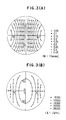
- Fig.2(A) is a graphical diagram showing the distribution of magnetic field on the region 30 in Fig.1. Curves on the diagram are plotted along equipotential surfaces and marked with the strength values of the magnetic field induced by the magnet 5 having a power of 2000 Gauss. By adjusting the power of the magnets 5 and 5 ⁇ , the strength of the magnetic field can be controlled so that the magnetic field becomes largely uniform over the surface to be coated which is located in the region 100 where the magnetic field (875 ⁇ 185 Gauss) and the electric field interact.
- a reference 26 designates the equipotential surface of 875 Gauss at which ECR (electron cyclotron resonance) condition between the magnetic field and the frequency of the microwave is sutisfied.
- ECR can not be establised due to the high pressure in the reaction chamber, 1-800 Torr, but instead a mixed cyclotron resonance (MCR) takes place in a broad region including the equipotential surface of the ECR condition.
- Fig.2(B) is a graphical diagram corresponding to Fig.2(A) and shows the strength of electric field of the microwave in the plasma generating space 1. The strength of the electric field takes its maximum value in the regions 100 and 100 ⁇ . However, in the region 100 ⁇ , it is difficult to heat the substrate 10 ⁇ without disturbing the propagation of the microwave. In other region. a film is not uniformly deposited, but deposited the product in the form of a doughnut.
- a uniform film can be formed on a circular substrate having a diameter of less than 100mm.
- a film is formed in the chamber on a circular substrate having a diameter of less than 50mm with a uniform thickness and a uniform quality.
- the diameter of the space 1 can be double by making use of 1.225 GHz as the frequency of the microwave.
- Figs.3(A) and 3(B) are graphical diagrams showing the distributions of the magnetic field and the electric field on a cross section of the plasma generating space 1. The curves ploted in the circles of the figures correspond equipotential surfaces. As shown in Fig.3(B), the electric field reaches its maxmum value at 25 KV/m.
- halo patterns were observed together with spots indicating the existence of diamond.
- the halo patterns gradually, which corresponds to an amorphous state, disappear as the substrate temperature elevates, and when the temperature rises beyond 650°C the film became a diamond.
- i-carbon film could not be formed.
- a film formation process was performed in the same manner as in the above but without using a magnetic field. As a result, a graphite film was deposited.
- polycrystalline silicon carbide films, and aluminium nitride films can be formed by making use of methyl silane, and alminium compound gas and ammonia gas respectively as a reactive gas. Further, other films having high melting points of tungsten, titanium, molybdenum or their silicon compounds can be formed in the similar manner.
- the apparatus comprises a reaction chamber in which a plasma generating space 1 and an auxiliary space 2 are defined and can be held at an appropriate pressure, a microwave generator 4, electro-magnets 5 and 5 ⁇ which are supplied with electric power from a power supply 25, and a water cooling system 18.
- the plasma generating space 1 has a circular cross section.
- a hollow cylinder 10 ⁇ having inward-turned brims is rotatably supported in the space so that a microwave emitted from the microwave genarator 4 passes through the cylinder along its axis.
- the cylinder 10 ⁇ is made of a stainless steel or a quartz and turned by means of a motor 16 through a gear.
- a evacuating system comprising a turbo molecular pump 8 and a rotary pump 14 which are connected with the reaction chamber through pressure controlling valves 11, 12 and 13. The process with this appratus is carried out as follow.
- Objects 10 to be coated for example, metallic, plastic, ceramic parts (such as gears, screws, ornament jigs, or micro-particles for grinding) are put in the cylinder 10 ⁇ and turned at 0.1-10 rpm during process.
- the cylinder 10 ⁇ although the means is not illustrated in the figure, is shaken by micro-vibration of 100Hz-10KHz. By the turning and the vibration, the surfaces of the objects exposed to the surrounding are always switching during process.
- the reaction chamber is evacuated by the turbo molecular pump 8 and the rotary pump to 1 x 10 ⁇ 6 Torr or lower.
- argon, helium or hydrogen as a non-productive gas is introduced to the reaction chamber from a gas introducing system 6 at 30SCCM, and a microwave of 2.45GHz is emitted from the microwave generator at 500 W through a microwave introduction window 15 to the plasma generating space 1 subjected to an magnetic field of about 2 K Gauss induced by the magnets 5 and 5 ⁇ .
- the pressure of the non-productive gas is 1 x 10 ⁇ 4Torr.
- a plasma is generated in the space 1 at a high density by the energy of the microwave.
- the surfaces of the objects 10 is cleaned by high energy electrons and non-productive atoms.
- C2H2, C2H4 and/or CH4 are introduced through a introduction system 7 at 1-800 Torr, preferably 3-30 Torr, e.g., 10 Torr, and excited by the energy of microwave in the same manner as carried out with the non-productive gas explained in the foregoing description.
- a heating means as illustrated in Fig.1 may be used as in Fig.1.
- halo patterns were obserbed together with spots indicating the existence of diamond.
- the halo patterns gradually disappear as the substrate temperature elevates, and when the temperature rises beyond 650°C the film became a diamond. At less than 150°C, i-carbon film could not be formed.
- a film formation process was performed in the same manner as in the above but without using a magnetic field. As a result, a graphite film was deposited.
- polycrystalline silicon carbide films, and aluminium nitride films can be formed by making use of methylsilane, and alminium compound gas and ammonia gas respectively as a reactive gas.
- other films having high melting points of tungsten, titanium, molybdenum or their silicon compounds can be formed in the similar manner.
- a BN or BP film could be formed in accordance with the present invention.
- the pressure in the reaction chamber is chosen at that required for ECR condition, so that a preliminary plasma discharge takes place. While the discharge continues, the pressure is changed to 1 Torr to 3 x 10³ Torr where a mixed resonance takes place with a plasma of which particles have a mean free path of 0.05 mm to several milimeters, normally not more than 1 mm.
- the process proposed by this invention is suitable for manufacturing superconducting ceramics including one or more rare earth elements, one or more alkaline earth element (including Be and Mg) and Cu.
- a process gas is prepared by bubbling a solution of compounds of the elements with oxygen gas.
- oxygen gas for example, an organic solution (benzene, or alcohol solution) or a water solution of alkylenes or halides of Y(OC2H5)3, Ba(OC2H5)3 and CuBr3 so that the stoichometric ratio among Y, Ba and Cu is 1:2:3.
- the stoichometric formula of the deposited product is YBa2Cu3O 6-8 .
- compounds of the elements can be inputted to the reaction chamber by blowing the compounds in the form of fine powder with a highly pressurized oxygen gas, so called spraying method.
- any hollow member having a cross section of a polygon can be employ.
- the embodiments employ microwave energy alone under the exsitence of magnetic field, photon energy can be applied to the reactive gas excited by a mixed resonance, on a position depart from the mixed resonance.
Abstract
Description
- This invention relates to a microwave enhanced method and an apparatus therefor.
- Recently, ECR CVD has attracted the interests of researchers as a new method of manufacturing thin films, particularly amorphous thin films. For example, Matsuo et al discloses one type of such a ECR CVD apparatus in USP 4,401,054. This recent technique utilizes microwaves to energize a reactive gas into a plasma state by virtue of a magnetic field which functions to pinch the plasma gas within the excitation space. With this configuration, the reactive gas can absorb the energy of the microwaves. A substrate to be coated is located distant from the excitation space (resonating space) for preventing the same from being spattered. The energized gas is showered on the substrate from the resonating space. In order to establish an electron cyclotron resonance, the pressure in a resonating space is kept at 1 x 10⁻³ to 1 x 10⁻⁵ Torr at which electrons can be considered as independent particle and resonate with a microwave in an electron cyclotron resonance on a certain surface on which the magnetic field takes a particular strength required for ECR. The excited plasma is extrated from the resonating space, by means of a divergent magnetic field, to a deposition space which is located distant from the resonating space and in which is disposed a substrate to be coated.
- In such a prior art method, it is very difficult to form a thin film of a polycrystalline or single-crystalline structure, so that currently available methods are almost limited to processes for manufacturing amourphous films. Also, high energy chemical vapor reaction is difficult to take place in accordance with such a prior art and therefore a diamond film or other films having high melting points, or uniform films on an even surface having depressions and caves can not be formed.
- It is therefore an object of the invention to provide a microwave enhanced CVD method and an apparatus therefor capable of forming a film, which can not be formed by prior art, such as a diamond film, or a film of a material having a high melting point.
- According to one aspect of the invention, the surface of an object to be coated is located in a region of a resonating space in which electric field of a microwave takes its maxmum value. By this configuration, the deposition can be carried out while the deposited film is being partially sputtered, and therefore, e.g., a diamond film can be formed.
- According to another aspect of the invention, a new CVD process has been culminated. The new process utilizes a mixed cyclotron resonance which was dirived firstly by the inventors. In the new type of exciting process, interaction of reactive gas itself must be taken into consideration as a non-negligible perturbation besides magnetic field and microwave, and therefore charged particles of a reactive gas can be absorbed in a relatively wide resonating space. For the mixed resonance, the pressure in a reaction chamber is elevated 10²-10⁵ times as high as that of prior art.
-
- Fig.1 is a cross section view showing a CVD apparatus in accordance with the present invention.
- Fig.2(A) is a graphical diagram showing the plofile of the equipotential surface of magnetic field in cross section.
- Fig.2(B) is a graphical diagram showing the strength of electric field.
- Figs.3(A) and 3(B) are graphical diagrams showing equipotential surfaces in terms of magnetic field and electric field respectively.
- Fig.4 is a cross section view showing another embodiment in accordance with the present invention.
- Referring to Fig.1, a microwave enhanced plasma CVD apparatus in accordance with the present invention is illustrated. In the figure, the apparatus comprises a reaction chamber in which a plasma generating space 1 and an
auxiliary space 2 are defined and can be held at an appropriate pressure, amicrowave genarator 4, electro-magnets 5 and 5ʹ in the form of solenoids surrounding the space 1, apower supply 25 for supplying and electric power to the electro-magnets 5 and 5ʹ, and awater cooling system 18. The plasma generating space 1 has a circular cross section. In the plasma generating space 1, a substrate holder 10ʹ made of a highly thermal conductive ceramic such as alminium nitride is provided on which asubstrate 10 is mounted. The substrate holder 10ʹ is irradiated and heated to 150-1000°C with an infrared light 24, which is emitted from anIR heater 20, reflected from an IR reflection parabola mirror 21 and focused on the back surface of the holder 10ʹ through alens 22. Areference numeral 23 designates a power supply for theIR heater 20. Provided for evacuating the reaction chamber is an evacuating system comprising a turbo molecular pump 8 and arotary pump 14 which are connected with the reaction chamber throughpressure controlling valves - A
substrate 10 is mounted on the substrate holder 10ʹ and heated by infrared light 24 to 500°C. Then, hydrogen gas is introduced from a gas introducing system 6 at 10 SCCM, and a microwave of 1 Kilo Gauss or stronger, e.g., 2.45GHz is emitted from the microwave generator thorugh amicrowave introduction window 15 to the plasma generating space 1 which is subjected to an magnetic field of about 2 K Gauss induced by themagnets 5 and 5ʹ. The hydrogen is excited in a high density plasma state in the space 1 by the energy of the microwave. The surface of the substrate is cleaned by high energy electrons and hydrogen atoms. In addition to the introduction of the hydrogen gas, C₂H₂ and CH₄ are inputted through aintroduction system 7, and excited by the energy of microwave at 1-800 Torr in the same manner as carried out with hydrogen explained in the foregoing description. As a result of a chemical vapor reaction, carbon is deposited in the form of a diamond film or an i-carbon (insulated carbon) film. The i-carbon is comprised of a mixture of diamond and amorphous carbon. - Fig.2(A) is a graphical diagram showing the distribution of magnetic field on the
region 30 in Fig.1. Curves on the diagram are plotted along equipotential surfaces and marked with the strength values of the magnetic field induced by themagnet 5 having a power of 2000 Gauss. By adjusting the power of themagnets 5 and 5ʹ, the strength of the magnetic field can be controlled so that the magnetic field becomes largely uniform over the surface to be coated which is located in theregion 100 where the magnetic field (875±185 Gauss) and the electric field interact. In the diagram, areference 26 designates the equipotential surface of 875 Gauss at which ECR (electron cyclotron resonance) condition between the magnetic field and the frequency of the microwave is sutisfied. Of course, in accordance with the present invention, ECR can not be establised due to the high pressure in the reaction chamber, 1-800 Torr, but instead a mixed cyclotron resonance (MCR) takes place in a broad region including the equipotential surface of the ECR condition. Fig.2(B) is a graphical diagram corresponding to Fig.2(A) and shows the strength of electric field of the microwave in the plasma generating space 1. The strength of the electric field takes its maximum value in theregions 100 and 100ʹ. However, in the region 100ʹ, it is difficult to heat the substrate 10ʹ without disturbing the propagation of the microwave. In other region. a film is not uniformly deposited, but deposited the product in the form of a doughnut. It is for this reason that thesubstrate 10 is disposed in thereason 100. The plasma flows in the lateral direction. According to the experimental, a uniform film can be formed on a circular substrate having a diameter of less than 100mm. Preferably, a film is formed in the chamber on a circular substrate having a diameter of less than 50mm with a uniform thickness and a uniform quality. When a lager substrate is desired to be coated, the diameter of the space 1 can be double by making use of 1.225 GHz as the frequency of the microwave. Figs.3(A) and 3(B) are graphical diagrams showing the distributions of the magnetic field and the electric field on a cross section of the plasma generating space 1. The curves ploted in the circles of the figures correspond equipotential surfaces. As shown in Fig.3(B), the electric field reaches its maxmum value at 25 KV/m. - The diffraction images of films formed in accordance with the present invention were obtained. As results, halo patterns were observed together with spots indicating the existence of diamond. The halo patterns gradually, which corresponds to an amorphous state, disappear as the substrate temperature elevates, and when the temperature rises beyond 650°C the film became a diamond. At less than 150°C, i-carbon film could not be formed. For reference, a film formation process was performed in the same manner as in the above but without using a magnetic field. As a result, a graphite film was deposited.
- In the same manner, polycrystalline silicon carbide films, and aluminium nitride films can be formed by making use of methyl silane, and alminium compound gas and ammonia gas respectively as a reactive gas. Further, other films having high melting points of tungsten, titanium, molybdenum or their silicon compounds can be formed in the similar manner.
- Referring to Fig.4, another embodiment of the invention is illustrated. In the figure, the apparatus comprises a reaction chamber in which a plasma generating space 1 and an
auxiliary space 2 are defined and can be held at an appropriate pressure, amicrowave generator 4, electro-magnets 5 and 5ʹ which are supplied with electric power from apower supply 25, and awater cooling system 18. The plasma generating space 1 has a circular cross section. In the plasma generating space 1, a hollow cylinder 10ʹ having inward-turned brims is rotatably supported in the space so that a microwave emitted from themicrowave genarator 4 passes through the cylinder along its axis. The cylinder 10ʹ is made of a stainless steel or a quartz and turned by means of amotor 16 through a gear. Provided for evacuating the reaction chamber is a evacuating system comprising a turbo molecular pump 8 and arotary pump 14 which are connected with the reaction chamber throughpressure controlling valves -
Objects 10 to be coated, for example, metallic, plastic, ceramic parts (such as gears, screws, ornament jigs, or micro-particles for grinding) are put in the cylinder 10ʹ and turned at 0.1-10 rpm during process. The cylinder 10ʹ, although the means is not illustrated in the figure, is shaken by micro-vibration of 100Hz-10KHz. By the turning and the vibration, the surfaces of the objects exposed to the surrounding are always switching during process. The reaction chamber is evacuated by the turbo molecular pump 8 and the rotary pump to 1 x 10⁻⁶ Torr or lower. Then, argon, helium or hydrogen as a non-productive gas is introduced to the reaction chamber from a gas introducing system 6 at 30SCCM, and a microwave of 2.45GHz is emitted from the microwave generator at 500 W through amicrowave introduction window 15 to the plasma generating space 1 subjected to an magnetic field of about 2 K Gauss induced by themagnets 5 and 5ʹ. The pressure of the non-productive gas is 1 x 10⁻⁴Torr. A plasma is generated in the space 1 at a high density by the energy of the microwave. The surfaces of theobjects 10 is cleaned by high energy electrons and non-productive atoms. In addition to the introduction of non-productive gas, C₂H₂, C₂H₄ and/or CH₄ are introduced through aintroduction system 7 at 1-800 Torr, preferably 3-30 Torr, e.g., 10 Torr, and excited by the energy of microwave in the same manner as carried out with the non-productive gas explained in the foregoing description. As a result of a mixed resonance, carbon is deposited in the form of a diamond film or an i-carbon film on theobjects 10. In this embodiment, a heating means as illustrated in Fig.1 may be used as in Fig.1. - The distributions of magnetic field and electric field are same as Figs.2(A), and 2(B), 3(A) and 3(B) explained in conjunction with the preceding embodiment, and therefore redundant descrip tion is dispensed with.
- The diffraction images of films formed in accordance with the present invention were obtained. As results, halo patterns were obserbed together with spots indicating the existence of diamond. The halo patterns gradually disappear as the substrate temperature elevates, and when the temperature rises beyond 650°C the film became a diamond. At less than 150°C, i-carbon film could not be formed. For reference, a film formation process was performed in the same manner as in the above but without using a magnetic field. As a result, a graphite film was deposited.
- In the same manner, polycrystalline silicon carbide films, and aluminium nitride films can be formed by making use of methylsilane, and alminium compound gas and ammonia gas respectively as a reactive gas. Further, other films having high melting points of tungsten, titanium, molybdenum or their silicon compounds can be formed in the similar manner. For example, a BN or BP film could be formed in accordance with the present invention.
- The pressure in the reaction chamber is chosen at that required for ECR condition, so that a preliminary plasma discharge takes place. While the discharge continues, the pressure is changed to 1 Torr to 3 x 10³ Torr where a mixed resonance takes place with a plasma of which particles have a mean free path of 0.05 mm to several milimeters, normally not more than 1 mm.
- The process proposed by this invention is suitable for manufacturing superconducting ceramics including one or more rare earth elements, one or more alkaline earth element (including Be and Mg) and Cu. In this case, a process gas is prepared by bubbling a solution of compounds of the elements with oxygen gas. For example, an organic solution (benzene, or alcohol solution) or a water solution of alkylenes or halides of Y(OC₂H₅)₃, Ba(OC₂H₅)₃ and CuBr₃ so that the stoichometric ratio among Y, Ba and Cu is 1:2:3. The stoichometric formula of the deposited product is YBa₂Cu₃O6-8. In place of bubbling method, compounds of the elements can be inputted to the reaction chamber by blowing the compounds in the form of fine powder with a highly pressurized oxygen gas, so called spraying method.
- The invention should not limited to the above particular embodiments and many modifications and variations may cause to those skilled in the art. For example, instead of the hollow cylinder, any hollow member having a cross section of a polygon can be employ. Although the embodiments employ microwave energy alone under the exsitence of magnetic field, photon energy can be applied to the reactive gas excited by a mixed resonance, on a position depart from the mixed resonance.
Claims (23)
a reaction chamber;
a gas feeding system for inputting a reactive gas into said reaction chamber;
a microwave generator connected with said reaction chamber to emit a microwave into a resonating space defined in said reaction chamber;
a magnet provided for inducing a magnetic field in said resonating space; and
means for holding an object to be coated in a region of said resonating space, the electric field of said microwave takeing its approximately maximum value within said region.
areaction chamber provided with means for evacuating said reaction chamber to a negative pressure;
means for generating a microwave in said reaction chamber; and
means for inducing a magnetic field in said reaction chamber;
said apparatus characterized in that an electron cyclotron resonance condition between the magnetic field and the microwave is established in a region where the electric field of said microwave takes its maximum value.
introducing a reactive gas into a reaction chamber;
inducing a magnetic field in said reaction chamber;
inputting a microwave into said reaction chamber;
exciting said reactive gas by said microwave under said magnetic field; and
depositing a film on a surface to be coated by a chemical vapor reaction,
said method characterized in that the deposition region is defined in the exciting region where said magnetic field and the microwave are cooperating with each other to excite said reactive gas.
introducing a reactive gas into a reaction chamber;
inducing a magnetic field in said reaction chamber;
inputting a microwave into said reaction chamber;
exciting said reactive gas with the energy of said microwave under said magnetic field; and
depositing a product on a surface to be coated by a chemical vapor reaction,
said method characterized in that the pressure of the reactive gas is kept between 1 Torr and 800 Torr during the process.
disposing an object to be processed in a reaction chamber;
inputting an reactive gas into said reaction chamber;
energizing the reactive gas by means of a microwave in cooperation with a magnetic field;
carring out a chemical vapor reaction on said object to be processed,
said method characterized in that the pressure of said reactive gas is chosen so that a mixed resonance takes place.
Applications Claiming Priority (4)
| Application Number | Priority Date | Filing Date | Title |
|---|---|---|---|
| JP266834/86 | 1986-11-10 | ||
| JP61266834A JPS63121667A (en) | 1986-11-10 | 1986-11-10 | Device and method for forming thin film |
| JP298/87 | 1987-01-05 | ||
| JP62000298A JPH0676665B2 (en) | 1987-01-05 | 1987-01-05 | Thin film formation method |
Publications (3)
| Publication Number | Publication Date |
|---|---|
| EP0267513A2 true EP0267513A2 (en) | 1988-05-18 |
| EP0267513A3 EP0267513A3 (en) | 1990-04-25 |
| EP0267513B1 EP0267513B1 (en) | 1998-08-12 |
Family
ID=26333254
Family Applications (1)
| Application Number | Title | Priority Date | Filing Date |
|---|---|---|---|
| EP87116091A Expired - Lifetime EP0267513B1 (en) | 1986-11-10 | 1987-11-02 | Microwave enhanced CVD method and apparatus |
Country Status (5)
| Country | Link |
|---|---|
| US (1) | US20050196549A1 (en) |
| EP (1) | EP0267513B1 (en) |
| KR (1) | KR930005010B1 (en) |
| CN (1) | CN1017726B (en) |
| DE (1) | DE3752208T2 (en) |
Cited By (6)
| Publication number | Priority date | Publication date | Assignee | Title |
|---|---|---|---|---|
| DE3742110A1 (en) * | 1986-12-12 | 1988-06-16 | Canon Kk | METHOD FOR FORMING FUNCTIONAL EVAPORATIVE FILMS BY A CHEMICAL MICROWAVE PLASMA EVAPORATION METHOD |
| EP0326405A2 (en) * | 1988-01-27 | 1989-08-02 | Semiconductor Energy Laboratory Co., Ltd. | Plasma chemical vapour reaction apparatus |
| EP0392125A1 (en) * | 1989-04-03 | 1990-10-17 | Shin-Etsu Chemical Co., Ltd. | Edged medical tool and method for preparation thereof |
| FR2658025A1 (en) * | 1990-02-07 | 1991-08-09 | Pelletier Jacques | Method and device for plasma treatment of articles of varied shape |
| GB2259185A (en) * | 1991-08-20 | 1993-03-03 | Bridgestone Corp | Method and apparatus for surface treatment |
| WO1996002934A1 (en) * | 1994-07-19 | 1996-02-01 | Ea Technology Limited | Method of and apparatus for microwave-plasma production |
Families Citing this family (1)
| Publication number | Priority date | Publication date | Assignee | Title |
|---|---|---|---|---|
| RU2762222C1 (en) * | 2019-11-05 | 2021-12-16 | Федеральное государственное бюджетное учреждение науки Институт общей физики им. А.М. Прохорова Российской академии наук (ИОФ РАН) | Uhf plasma reactor with regulation of temperature of indirect substrate heating |
Citations (3)
| Publication number | Priority date | Publication date | Assignee | Title |
|---|---|---|---|---|
| EP0046945A1 (en) * | 1980-08-22 | 1982-03-10 | Kabushiki Kaisha Toshiba | Method and apparatus for treating fluorescent substance |
| US4401054A (en) * | 1980-05-02 | 1983-08-30 | Nippon Telegraph & Telephone Public Corporation | Plasma deposition apparatus |
| US4559100A (en) * | 1983-12-23 | 1985-12-17 | Hitachi, Ltd. | Microwave plasma etching apparatus |
Family Cites Families (19)
| Publication number | Priority date | Publication date | Assignee | Title |
|---|---|---|---|---|
| DE1900116C3 (en) * | 1969-01-02 | 1978-10-19 | Siemens Ag, 1000 Berlin Und 8000 Muenchen | Process for the production of high-purity monocrystalline layers consisting of silicon |
| US3911318A (en) * | 1972-03-29 | 1975-10-07 | Fusion Systems Corp | Method and apparatus for generating electromagnetic radiation |
| US4047496A (en) * | 1974-05-31 | 1977-09-13 | Applied Materials, Inc. | Epitaxial radiation heated reactor |
| JPS5779621A (en) * | 1980-11-05 | 1982-05-18 | Mitsubishi Electric Corp | Plasma processing device |
| JPH0635323B2 (en) * | 1982-06-25 | 1994-05-11 | 株式会社日立製作所 | Surface treatment method |
| DE3369772D1 (en) * | 1982-07-31 | 1987-03-12 | Bbc Brown Boveri & Cie | Multifilament superconductor and method of making the same |
| US4513684A (en) * | 1982-12-22 | 1985-04-30 | Energy Conversion Devices, Inc. | Upstream cathode assembly |
| JPS59159167A (en) * | 1983-03-01 | 1984-09-08 | Zenko Hirose | Manufacture of amorphous silicon film |
| JPS59222922A (en) * | 1983-06-01 | 1984-12-14 | Nippon Telegr & Teleph Corp <Ntt> | Vapor growth apparatus |
| JPS6037129A (en) * | 1983-08-10 | 1985-02-26 | Hitachi Ltd | Equipment for manufacturing semiconductor |
| JPS60170234A (en) * | 1984-02-15 | 1985-09-03 | Semiconductor Energy Lab Co Ltd | Vapor-phase reaction apparatus and manufacture of vapor-phase reaction film |
| US4727293A (en) * | 1984-08-16 | 1988-02-23 | Board Of Trustees Operating Michigan State University | Plasma generating apparatus using magnets and method |
| US4640224A (en) * | 1985-08-05 | 1987-02-03 | Spectrum Cvd, Inc. | CVD heat source |
| US4776918A (en) * | 1986-10-20 | 1988-10-11 | Hitachi, Ltd. | Plasma processing apparatus |
| US6677001B1 (en) * | 1986-11-10 | 2004-01-13 | Semiconductor Energy Laboratory Co., Ltd. | Microwave enhanced CVD method and apparatus |
| US5266363A (en) * | 1986-11-10 | 1993-11-30 | Semiconductor Energy Laboratory Co., Ltd. | Plasma processing method utilizing a microwave and a magnetic field at high pressure |
| DE3853890T2 (en) * | 1987-01-19 | 1995-10-19 | Hitachi Ltd | Device working with a plasma. |
| KR900008505B1 (en) * | 1987-02-24 | 1990-11-24 | 세미콘덕터 에너지 라보라터리 캄파니 리미티드 | Microwave enhanced cvd method for depositing carbon |
| KR910007384B1 (en) * | 1987-09-16 | 1991-09-25 | 가부시끼가이샤 한도다이 에네르기 겐뀨쇼 | Formation of superconductor oxide film |
-
1987
- 1987-11-02 DE DE3752208T patent/DE3752208T2/en not_active Expired - Fee Related
- 1987-11-02 EP EP87116091A patent/EP0267513B1/en not_active Expired - Lifetime
- 1987-11-06 KR KR1019870012471A patent/KR930005010B1/en not_active IP Right Cessation
- 1987-11-09 CN CN87107779A patent/CN1017726B/en not_active Expired
-
2005
- 2005-04-11 US US11/102,651 patent/US20050196549A1/en not_active Abandoned
Patent Citations (3)
| Publication number | Priority date | Publication date | Assignee | Title |
|---|---|---|---|---|
| US4401054A (en) * | 1980-05-02 | 1983-08-30 | Nippon Telegraph & Telephone Public Corporation | Plasma deposition apparatus |
| EP0046945A1 (en) * | 1980-08-22 | 1982-03-10 | Kabushiki Kaisha Toshiba | Method and apparatus for treating fluorescent substance |
| US4559100A (en) * | 1983-12-23 | 1985-12-17 | Hitachi, Ltd. | Microwave plasma etching apparatus |
Non-Patent Citations (1)
| Title |
|---|
| JAPANESE JOURNAL OF APPLIED PHYSICS, vol. 26, no. 6, June 1987, pages L1032-L1034, Tokyo, JP; H. KAWARADA et al.: "Large area chemical vapour deposition of diamond particles and films using magneto-microwave plasma" * |
Cited By (12)
| Publication number | Priority date | Publication date | Assignee | Title |
|---|---|---|---|---|
| DE3742110A1 (en) * | 1986-12-12 | 1988-06-16 | Canon Kk | METHOD FOR FORMING FUNCTIONAL EVAPORATIVE FILMS BY A CHEMICAL MICROWAVE PLASMA EVAPORATION METHOD |
| EP0326405A2 (en) * | 1988-01-27 | 1989-08-02 | Semiconductor Energy Laboratory Co., Ltd. | Plasma chemical vapour reaction apparatus |
| EP0326405A3 (en) * | 1988-01-27 | 1989-11-02 | Sel Semiconductor Energy Laboratory Co., Ltd. | Plasma chemical vapour reaction apparatus |
| EP0392125A1 (en) * | 1989-04-03 | 1990-10-17 | Shin-Etsu Chemical Co., Ltd. | Edged medical tool and method for preparation thereof |
| FR2658025A1 (en) * | 1990-02-07 | 1991-08-09 | Pelletier Jacques | Method and device for plasma treatment of articles of varied shape |
| GB2259185A (en) * | 1991-08-20 | 1993-03-03 | Bridgestone Corp | Method and apparatus for surface treatment |
| US5316739A (en) * | 1991-08-20 | 1994-05-31 | Bridgestone Corporation | Method and apparatus for surface treatment |
| GB2259185B (en) * | 1991-08-20 | 1995-08-16 | Bridgestone Corp | Method and apparatus for surface treatment |
| WO1996002934A1 (en) * | 1994-07-19 | 1996-02-01 | Ea Technology Limited | Method of and apparatus for microwave-plasma production |
| GB2307099A (en) * | 1994-07-19 | 1997-05-14 | Ea Tech Ltd | Method of and apparatus for microwave-plasma production |
| GB2307099B (en) * | 1994-07-19 | 1997-11-26 | Ea Tech Ltd | Method of and apparatus for microwave-plasma production |
| US5874705A (en) * | 1994-07-19 | 1999-02-23 | Ea Technology Limited | Method of and apparatus for microwave-plasma production |
Also Published As
| Publication number | Publication date |
|---|---|
| DE3752208T2 (en) | 1998-12-24 |
| CN87107779A (en) | 1988-05-25 |
| KR930005010B1 (en) | 1993-06-11 |
| DE3752208D1 (en) | 1998-09-17 |
| US20050196549A1 (en) | 2005-09-08 |
| EP0267513A3 (en) | 1990-04-25 |
| EP0267513B1 (en) | 1998-08-12 |
| CN1017726B (en) | 1992-08-05 |
| KR880006959A (en) | 1988-07-25 |
Similar Documents
| Publication | Publication Date | Title |
|---|---|---|
| US5015494A (en) | Microwave enhanced CVD method for depositing diamond | |
| US6110542A (en) | Method for forming a film | |
| US4871581A (en) | Carbon deposition by ECR CVD using a catalytic gas | |
| US6423383B1 (en) | Plasma processing apparatus and method | |
| US5013579A (en) | Microwave enhanced CVD method for coating mechanical parts for improved wear resistance | |
| US5039548A (en) | Plasma chemical vapor reaction method employing cyclotron resonance | |
| US5601883A (en) | Microwave enhanced CVD method for coating plastic with carbon films | |
| US5203959A (en) | Microwave plasma etching and deposition method employing first and second magnetic fields | |
| US4973883A (en) | Plasma processing apparatus with a lisitano coil | |
| US20050196549A1 (en) | Microwave enhanced CVD method and apparatus | |
| EP0284436B1 (en) | Substrate-treating apparatus | |
| US5183685A (en) | Diamond film deposition by ECR CVD using a catalyst gas | |
| US5266363A (en) | Plasma processing method utilizing a microwave and a magnetic field at high pressure | |
| US6677001B1 (en) | Microwave enhanced CVD method and apparatus | |
| EP0772699B1 (en) | Cvd process for the production of diamond-phase carbon tubes | |
| US5270029A (en) | Carbon substance and its manufacturing method | |
| EP0556615B1 (en) | Method of making synthetic diamond | |
| US5277939A (en) | ECR CVD method for forming BN films | |
| JPH0420985B2 (en) | ||
| JP2617539B2 (en) | Equipment for producing cubic boron nitride film | |
| JPH031377B2 (en) | ||
| JPS63169387A (en) | Formation of thin film | |
| JP3291274B2 (en) | Carbon coating method | |
| JP2739286B2 (en) | Plasma processing method | |
| JPH0676665B2 (en) | Thin film formation method |
Legal Events
| Date | Code | Title | Description |
|---|---|---|---|
| PUAI | Public reference made under article 153(3) epc to a published international application that has entered the european phase |
Free format text: ORIGINAL CODE: 0009012 |
|
| AK | Designated contracting states |
Kind code of ref document: A2 Designated state(s): DE FR GB |
|
| PUAL | Search report despatched |
Free format text: ORIGINAL CODE: 0009013 |
|
| AK | Designated contracting states |
Kind code of ref document: A3 Designated state(s): DE FR GB |
|
| 17P | Request for examination filed |
Effective date: 19901025 |
|
| 17Q | First examination report despatched |
Effective date: 19930128 |
|
| GRAG | Despatch of communication of intention to grant |
Free format text: ORIGINAL CODE: EPIDOS AGRA |
|
| GRAG | Despatch of communication of intention to grant |
Free format text: ORIGINAL CODE: EPIDOS AGRA |
|
| GRAH | Despatch of communication of intention to grant a patent |
Free format text: ORIGINAL CODE: EPIDOS IGRA |
|
| GRAH | Despatch of communication of intention to grant a patent |
Free format text: ORIGINAL CODE: EPIDOS IGRA |
|
| GRAA | (expected) grant |
Free format text: ORIGINAL CODE: 0009210 |
|
| AK | Designated contracting states |
Kind code of ref document: B1 Designated state(s): DE FR GB |
|
| REF | Corresponds to: |
Ref document number: 3752208 Country of ref document: DE Date of ref document: 19980917 |
|
| ET | Fr: translation filed | ||
| PLBE | No opposition filed within time limit |
Free format text: ORIGINAL CODE: 0009261 |
|
| STAA | Information on the status of an ep patent application or granted ep patent |
Free format text: STATUS: NO OPPOSITION FILED WITHIN TIME LIMIT |
|
| 26N | No opposition filed | ||
| PGFP | Annual fee paid to national office [announced via postgrant information from national office to epo] |
Ref country code: GB Payment date: 20011102 Year of fee payment: 15 |
|
| PGFP | Annual fee paid to national office [announced via postgrant information from national office to epo] |
Ref country code: FR Payment date: 20011122 Year of fee payment: 15 |
|
| PGFP | Annual fee paid to national office [announced via postgrant information from national office to epo] |
Ref country code: DE Payment date: 20011214 Year of fee payment: 15 |
|
| REG | Reference to a national code |
Ref country code: GB Ref legal event code: IF02 |
|
| PG25 | Lapsed in a contracting state [announced via postgrant information from national office to epo] |
Ref country code: GB Free format text: LAPSE BECAUSE OF NON-PAYMENT OF DUE FEES Effective date: 20021102 |
|
| PG25 | Lapsed in a contracting state [announced via postgrant information from national office to epo] |
Ref country code: DE Free format text: LAPSE BECAUSE OF NON-PAYMENT OF DUE FEES Effective date: 20030603 |
|
| GBPC | Gb: european patent ceased through non-payment of renewal fee | ||
| PG25 | Lapsed in a contracting state [announced via postgrant information from national office to epo] |
Ref country code: FR Free format text: LAPSE BECAUSE OF NON-PAYMENT OF DUE FEES Effective date: 20030731 |
|
| REG | Reference to a national code |
Ref country code: FR Ref legal event code: ST |