EP0269174A2 - Logic circuit for expansion of monochrome display patterns to color form and video controller comprising such logic circuit - Google Patents
Logic circuit for expansion of monochrome display patterns to color form and video controller comprising such logic circuit Download PDFInfo
- Publication number
- EP0269174A2 EP0269174A2 EP87202226A EP87202226A EP0269174A2 EP 0269174 A2 EP0269174 A2 EP 0269174A2 EP 87202226 A EP87202226 A EP 87202226A EP 87202226 A EP87202226 A EP 87202226A EP 0269174 A2 EP0269174 A2 EP 0269174A2
- Authority
- EP
- European Patent Office
- Prior art keywords
- latch
- source
- image
- register
- destination
- Prior art date
- Legal status (The legal status is an assumption and is not a legal conclusion. Google has not performed a legal analysis and makes no representation as to the accuracy of the status listed.)
- Withdrawn
Links
Images
Classifications
-
- G—PHYSICS
- G09—EDUCATION; CRYPTOGRAPHY; DISPLAY; ADVERTISING; SEALS
- G09G—ARRANGEMENTS OR CIRCUITS FOR CONTROL OF INDICATING DEVICES USING STATIC MEANS TO PRESENT VARIABLE INFORMATION
- G09G5/00—Control arrangements or circuits for visual indicators common to cathode-ray tube indicators and other visual indicators
- G09G5/02—Control arrangements or circuits for visual indicators common to cathode-ray tube indicators and other visual indicators characterised by the way in which colour is displayed
- G09G5/024—Control arrangements or circuits for visual indicators common to cathode-ray tube indicators and other visual indicators characterised by the way in which colour is displayed using colour registers, e.g. to control background, foreground, surface filling
Definitions
- This invention pertains to the general field of video display controllers or raster scan display controllers which are used in computer system.
- it pertains to a logic circuit which is used to expand a monochrome image to a color image while minimizing memory storage requirements for a multicolor display.
- Most presently available video display systems include a processor, a video controller, a display memory containing a single actual screen image, further system memory, and a raster scan video display.
- the video controller In normal or steady-state operation, the video controller continually reads out the contents of the display memory and transforms the information read into signals which control the raster scan beam during its active display time.
- the video controller also provides the horizontal and vertical retrace signals at appropriate intervals, and blanking of the raster scan beam during retrace.
- the processor also has access to the display memory, so that it can change the actual screen image. This access may either be "through” the video controller or "around” it.
- the subject invention applies to the former type of system. In either case, use of the display memory typically involves careful control of updating accesses and display accesses to prevent image breakup while the video image is being changed.
- An improved video controller incorporating the present invention is a logic circuit which has an address module and at least one data module.
- the controller is designed to work with an external processor which generates the necessary instructions.
- the major function of the address module is to generate both video addresses and update addresses, while the data modules are used to collect and integrate video data that have been read out from the display memory.
- the data output from the data module passes through high speed shift registers and a look-up table to a CRT display.
- the major parts of the address module are a synchronous signal generator, a window controller, an update controller and an interface controller.
- the address module also has the ability to update the contents of the display memory according to instructions passed from the host system. Thus, the host system itself does not have to access display memory to insert characters or graphic elements into display memory. It only passes the appropriate instructions and/or data to the controller.
- the present application pertains to a novel feature in the update controller.
- the controller can be programmed to express a -zero- in the source pattern in either of two ways: a) by changing the corresponding pixel to the color code previously programmed into a background color latch, or b) by leaving the corresponding pixel unchanged.
- a) by changing the corresponding pixel to the color code previously programmed into a background color latch or b) by leaving the corresponding pixel unchanged.
- the former mode of operation the entire region of the screen occupied by the image is changed to a new foreground/background image.
- the image is drawn "over" a preexisting background.
- the operation is controlled by foreground color and background color registers, each of which has the number of bits needed to represent one pixel color code; the BPP register, which defines the number of bits per pixel; and a single bit register, write/overlay, which determines whether or not the background is to be changed.
- a control unit begins active operation by fetching one word of the monochrome source pattern from the display memory and strobing it into a "Source Latch" in the expander.
- the function of the expander is to convert this source pattern into 1, 2, 4 or 8 words on its output.
- a programmed logic array in the expander performs this expansion by taking the word from the source latch, the contents of BPP (how much to expand), and the contents of register CT (which controls which word of a multi-word expansion is being done).
- a 4-to-1 multiplexer produces the "empty" output which tells the control unit when a new word must be fetched from the source pattern.
- the control unit then fetches a word from the destination pattern and strobes it into the destination latch in the pattern generator.
- a smart control unit could omit this step, except for the first and last word of a scan line.
- a 2-to-1 multiplexer then selects between the destination data and the background latch, under control of a write/overlay register bit. For each bit, the corresponding output from the expander controls whether the display output is from the foreground latch or the 2-to-1 multiplexer. The resulting display is then colored and/or expanded according to the preprogrammed parameters.
- the expansion of a monochrome image pattern to a multicolor form and/or the horizontal expansion of a character/image is programmable by the user and effected by a logical circuit. Furthermore, the same expansion circuitry is used for any level expansion. This feature adds flexibility to the system and widens its applicability. Although hereinafter, a CRT-display is described, other color display technologies would be applicable.
- a bit-mapped raster scan video (CRT) controller has an address module and a data module.
- This controller provides hardware support for windows in a bit-mapped alphanumeric and graphic raster scan video (CRT) display system used in a computer system having one or more main processors and is particularly advantageous for use with multitasking operating systems. It typically includes logical circuits whereby a description of overlapping windows can be programmed.
- the major parts of the address module are a synchronous signal generator, a window controller, an update controller and an interface controller. This application is directed primarily to the update controller of the address module.
- the major function of the address module is to generate both video addresses and update addresses, while the data modules are used to collect and integrate the display patterns that have been read out from the display memory. The data output by the data module(s) then goes through high speed shift register(s) and color look-up tables to the video display.
- the address module also has the ability to update the contents of the display memory according to the instructions passed from the host system. Therefore, the host processor does not have to access the display memory when it wants to insert some characters or graphic elements into the display memory. Instead, it only needs to pass appropriate instructions to the address module.
- the address module After receiving the instructions passed from the host system, the address module executes them one by one like a special purpose microprocessor. Since the whole procedure is controlled by the internal hardware, updating can be done within a very short time. Typically the insertion speed is 5 to 50 times faster than a software procedure on the host processor.
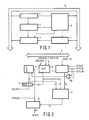
- Figure 1 shows the block structures of an Update Controller. It comprises an Expander 1, Pattern Shifter 2, Mask Generator 3, Pattern Generator 4, and Update Control Unit 5, and is connected to internal bus 6.
- the Update Control Unit 5 is used to update the display memory according to the instructions passed to it from the host system.
- the main update function provided by the Update Control Unit 5 is to insert characters and graphics elements into the display memory.
- a block move can be implemented as a special case of character insertion. In this mode, operation is similar to a monochrome character insertion operation.
- the expander may be used in a monochrome display mode to magnify the display patterns in the horizontal direction by a "zoom" factor of either 2, 4 or 8 times.
- Source words are read from display memory (not shown) via Internal Data Bus 6 and placed in a Source Latch 7.
- Each source word has 16 bits and represents a part of an overall monochrome pattern that can either be expanded to a color form with 2, 4 or 8 bits per pixel or can be left in its incoming monochrome form with 1 bit per pixel.
- BPP latch 8 The choice among these four alternative functions is determined by the preprogrammed contents of a BPP latch 8. This latch has 2 bits; its contents are encoded as follows:
- the process of inserting a bit-mapped pattern into display memory may be divided into one or more major sections which correspond to successive scan lines on the screen. Each such major section is further divided into one or more successive 16-bit "destination words".
- a CT Counter 9 and 4-to-1 Multiplexer 11 function together to inform the Update Control Unit 5 when a new source word is needed by generating a signal named UEEMP which is fed back to the Update Control Unit 5.
- the CT Counter 9 is a 4-bit binary counter which is cleared whenever the Update Control Unit 5 loads a source word into Source Latch 7.
- the clear signal is produced by OR-gate 6 that combines the write and reset signals for Source Latch 7.
- the counter is incremented by 1 for each destination word that is processed and written back to memory.
- the 4-to-1 Multiplexer 11 has as its data inputs the four output bits of CT Counter 9 and the two outputs of the BPP Latch 8 as its control inputs. It functions as indicated in Table 2. Thus, when UEEMP is 1, it is a signal to the Update Control Unit 5 that a new source word is needed.
- Expansion Logic 12 takes as its inputs the 16 outputs of Source Latch 10, the 2 outputs of the BPP latch 8, and the three less-significant outputs of the CT counter 9. It uses these to divide the source word into 1, 2, 4 or 8 equal segments having 16, 8, 4 or 2 bits each respectively, depending on the BPP value. Each such segment corresponds to one destination word, and for each segment the Expansion Logic produces a 16-bit word at its outputs, having 1, 2, 4 or 8 consecutive bits (respectively) equal to the value of 1 bit of the segment.
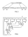
- the operation of the Expansion Logic 12 is exemplified in Figure 3, for a BPP value of 10, that is, 4 bits/pixel.
- the Expansion Logic can be a set of logic gates or a Programmable Logic Array (PLA). In either case, the Expansion Logic operates according to the logic equations in Tables 3a, 3b.
- PLA Programmable Logic Array
- CT0 is the least-significant bit from the CT counter 8 thru CT3 is the most-significant bit from the CT counter 8 I0 is the least-significant bit from the source latch 6 thru I15 is the most-signficiant bit from the source latch 6 BBP0 is the less-significant bit from the BPP latch 7 BBP1 is the more-significant bit from the BPP latch 7
- the outputs of the Expansion Logic are stored in a 16-bit Latch 13, and are captured therein at the same time the CT Counter 9 is signalled to increment, that is, once for each destination word processed and written into memory.
- the outputs of Latch 13 constitute the output of the Expander 1 to the Pattern Shifter 2.
- the Pattern Shifter 2 aligns the output of the Expander 1 to correspond to "destination" data read from display memory. This function is not necessary to implement the present invention. For clarity of explanation, the Pattern Shifter is herein assumed to propagate the output from the Expander 1 to the Pattern Generator 4, without change.
- the pattern to be inserted into display memory can start and end at any pixel on the screen, and can be any number of pixels in width, it is typical for part of the first and last destination words of each major section to remain unchanged by the insertion process.
- the function of the Mask Generator 3 is to produce the bit patterns required for proper operation of the Pattern Generator 4, so that such parts of such first and last destination words remain unchanged. However, this function is also not necessary to implement the present invention.
- the pattern to be inserted does indeed affect the entire first and last destination words of each major section, in which case the Mask Generator 3 outputs all zeroes to the Pattern Generator 4.
- the Pattern Generator 4 combines, for each destination word in each major section, some or all of the following information:
- Figure 4 shows details of the Pattern Generator 4.
- certain registers are preprogrammed (e.g., by a system microprocessor).
- Write/Overlay Register 55 is programmed to the "Write” state if pixels corresponding to zeroes in the monochrome are to be changed to the contents of the Background Color Register, or to the "Overlay” state if such pixels are to be left unchanged in display memory.
- Foreground Color Register 54 is programmed to contain the value to which pixels corresponding to -ones- in the monochrome pattern are to be changed. If Write/Overlay Register 55 is programmed to "Write", then Background Color Register 53 is programmed to contain the value to which pixels corresponding to zeroes in the monochrome pattern are to be changed.
- both the Color Registers 53 and 54 are implemented as 8 bits wide. Because the major data paths of the Pattern Generator are 16 bits wide, the outputs of these registers are replicated twice into the inputs of Multiplexers 56 and 58 respectively. If the number of destination bits/pixel is 4, 2 or 1, then the Color Registers are typically programmed with the desired pixel value replicated 2, 4 or 8 times, respectively, but alternatively in this case, various graphic-pattern effects can be produced on the screen by programming the 2, 4 or 8 pixels in a Color Register to different values.
- the Update Control Unit 5 operating via the Interface Controller (not shown), reads one word from memory and places the data therefrom into the Source Latch 7, for each 8, 4, 2 or 1 destination words written into memory. For each such destination word, the Update Control Unit 5 may read the data from the word and place the data therefrom into the Destination Latch Register 52.
- the invention applies to both a simple embodiment of an Update Control Unit 5, which always reads each destination word from memory, and to a more complex and efficient embodiment which uses additional signals from the other blocks, so as to omit this step of reading a destination word if/when its contents are not needed to form the new contents for the word.
- Two-to-one Multiplexer 56 selects between existent destination pixels from the Destination Latch 52, or the pixels from the Background Color Register 53, all 16 of its bits or stages being controlled by the common signal from the Write/Overlay Register 55.
- the output of Multiplexer 56 may be characterized as the "effective background" that is used for pixels corresponding to zeroes in the monochrome pattern.
- Mutliplexer 57 propagates the "expanded and shifted" source data from the Pattern Shifter 2 to its outputs.
- Two-to-one Multiplexer 58 selects between the "effective background" from Multiplexer 56, and the pixels from the Foreground Color Register 54, each of its bits or stages being individually controlled by the corresponding bit from Multiplexer 57.
- the selection for each bit is, in effect, controlled by the Pattern Shifter 2, the Expander 1, and ultimately by one of the monochrome bits in the Source Latch 7.
- the output of Multiplexer 58 may be characterized as the integration of the foreground and background parts of the pattern.
- Two-to-one Multiplexer 59 selects between the output of Multiplexer 58 and the output of Destination Latch 13, each of its bits of stages being individually controlled by the corresponding bit from the Mask Generator 3. This multiplexer handles the preservation of "unaffected" pixels in the first and last destination words for each scan line. For clarity in describing the invention, Multiplexer 59 can be assumed to propagate the data from Multiplexer 58 to its outputs.
- the Drivers 60 are controlled by the Update Control Unit 5 so as to place the result from Multiplexer 59 on the internal bus 6, at the appropriate time so that it is propagated to the device's external data pins, and ultimately written to the destination word in display memory.
- the Update Control Unit 5 controls the repetition of this process for each destination word in each scan line of the monochrome pattern, reading new source words from the monochrome pattern as needed.
- the invention is generally applicable to any 3-way multiplexing scheme among existing destination data and two preprogrammed constant registers, said multiplexing controlled by a single write/overlay control bit and a plurality of foreground/background control bits that are derived from expanding a monochrome pattern by the method described herein.
Abstract
Description
- This invention pertains to the general field of video display controllers or raster scan display controllers which are used in computer system. In particular it pertains to a logic circuit which is used to expand a monochrome image to a color image while minimizing memory storage requirements for a multicolor display.
- Most presently available video display systems include a processor, a video controller, a display memory containing a single actual screen image, further system memory, and a raster scan video display. In normal or steady-state operation, the video controller continually reads out the contents of the display memory and transforms the information read into signals which control the raster scan beam during its active display time. The video controller also provides the horizontal and vertical retrace signals at appropriate intervals, and blanking of the raster scan beam during retrace.
- The processor also has access to the display memory, so that it can change the actual screen image. This access may either be "through" the video controller or "around" it. The subject invention applies to the former type of system. In either case, use of the display memory typically involves careful control of updating accesses and display accesses to prevent image breakup while the video image is being changed.
- An improved video controller incorporating the present invention is a logic circuit which has an address module and at least one data module. The controller is designed to work with an external processor which generates the necessary instructions. The major function of the address module is to generate both video addresses and update addresses, while the data modules are used to collect and integrate video data that have been read out from the display memory. The data output from the data module passes through high speed shift registers and a look-up table to a CRT display. The major parts of the address module are a synchronous signal generator, a window controller, an update controller and an interface controller. The address module also has the ability to update the contents of the display memory according to instructions passed from the host system. Thus, the host system itself does not have to access display memory to insert characters or graphic elements into display memory. It only passes the appropriate instructions and/or data to the controller. The present application pertains to a novel feature in the update controller.
- In color CRT systems with two or more memory bits per pixel, many images/shapes/characters are shown in only one particular color. Such images can be defined by a pattern with one bit per pixel (1 = part of image, 0 = not part of image). When the display on a CRT screen is updated by a controller, the most typical operation is to display a shape/image/character on the screen in a single color. The shape is defined by a source monochrome pattern which is stored in display memory and has one bit per pixel. A -one- in the bit corresponding to a particular destination pixel indicates that the pixel is part of an image and should be displayed with a color code previously programmed in a foreground color latch. This invention expands such patterns into n-bit per pixel color form, with a programmable image color and an optional programmable background color. This minimizes memory requirements for storing patterns, and reduces the time needed to place the image on the screen.
- The controller can be programmed to express a -zero- in the source pattern in either of two ways: a) by changing the corresponding pixel to the color code previously programmed into a background color latch, or b) by leaving the corresponding pixel unchanged. In the former mode of operation the entire region of the screen occupied by the image is changed to a new foreground/background image. In the latter mode, the image is drawn "over" a preexisting background. The operation is controlled by foreground color and background color registers, each of which has the number of bits needed to represent one pixel color code; the BPP register, which defines the number of bits per pixel; and a single bit register, write/overlay, which determines whether or not the background is to be changed.
- Before active operation begins, all of these registers are loaded (e.g. by a microprocessor) with the desired values. Also, a counter in the expander is cleared to contain the
value 0. A control unit begins active operation by fetching one word of the monochrome source pattern from the display memory and strobing it into a "Source Latch" in the expander. The function of the expander is to convert this source pattern into 1, 2, 4 or 8 words on its output. A programmed logic array in the expander performs this expansion by taking the word from the source latch, the contents of BPP (how much to expand), and the contents of register CT (which controls which word of a multi-word expansion is being done). A 4-to-1 multiplexer produces the "empty" output which tells the control unit when a new word must be fetched from the source pattern. - The control unit then fetches a word from the destination pattern and strobes it into the destination latch in the pattern generator. When both foreground and background are being changed, a smart control unit could omit this step, except for the first and last word of a scan line. A 2-to-1 multiplexer then selects between the destination data and the background latch, under control of a write/overlay register bit. For each bit, the corresponding output from the expander controls whether the display output is from the foreground latch or the 2-to-1 multiplexer. The resulting display is then colored and/or expanded according to the preprogrammed parameters.
- Thus, in the present invention, the expansion of a monochrome image pattern to a multicolor form and/or the horizontal expansion of a character/image is programmable by the user and effected by a logical circuit. Furthermore, the same expansion circuitry is used for any level expansion. This feature adds flexibility to the system and widens its applicability. Although hereinafter, a CRT-display is described, other color display technologies would be applicable.
- A preferred embodiment of the invention will be described with respect to the following Figures, wherein
- Figure 1 is a block diagram of an Update Controller subsystem of a raster scan video controller using the invention;
- Figure 2 is a detail of the Expander block shown in Figure 1;
- Figure 3 exemplifies the operation of the Expander for the particular case of four bits per pixel;
- Figure 5 shows portions of the Pattern Generator block of Figure 1.
- A bit-mapped raster scan video (CRT) controller has an address module and a data module. This controller provides hardware support for windows in a bit-mapped alphanumeric and graphic raster scan video (CRT) display system used in a computer system having one or more main processors and is particularly advantageous for use with multitasking operating systems. It typically includes logical circuits whereby a description of overlapping windows can be programmed.
- The major parts of the address module are a synchronous signal generator, a window controller, an update controller and an interface controller. This application is directed primarily to the update controller of the address module. The major function of the address module is to generate both video addresses and update addresses, while the data modules are used to collect and integrate the display patterns that have been read out from the display memory. The data output by the data module(s) then goes through high speed shift register(s) and color look-up tables to the video display.
- The address module also has the ability to update the contents of the display memory according to the instructions passed from the host system. Therefore, the host processor does not have to access the display memory when it wants to insert some characters or graphic elements into the display memory. Instead, it only needs to pass appropriate instructions to the address module.
- After receiving the instructions passed from the host system, the address module executes them one by one like a special purpose microprocessor. Since the whole procedure is controlled by the internal hardware, updating can be done within a very short time. Typically the insertion speed is 5 to 50 times faster than a software procedure on the host processor.
- Figure 1 shows the block structures of an Update Controller. It comprises an Expander 1, Pattern Shifter 2,
Mask Generator 3, Pattern Generator 4, andUpdate Control Unit 5, and is connected tointernal bus 6. TheUpdate Control Unit 5 is used to update the display memory according to the instructions passed to it from the host system. The main update function provided by theUpdate Control Unit 5 is to insert characters and graphics elements into the display memory. A block move can be implemented as a special case of character insertion. In this mode, operation is similar to a monochrome character insertion operation. The expander may be used in a monochrome display mode to magnify the display patterns in the horizontal direction by a "zoom" factor of either 2, 4 or 8 times. - Details of the Expander 1 are shown in Figure 2. Under control of the
Update Control Unit 5 and an Interface Controller (not shown), "source words" are read from display memory (not shown) viaInternal Data Bus 6 and placed in a Source Latch 7. Each source word has 16 bits and represents a part of an overall monochrome pattern that can either be expanded to a color form with 2, 4 or 8 bits per pixel or can be left in its incoming monochrome form with 1 bit per pixel. - The choice among these four alternative functions is determined by the preprogrammed contents of a
BPP latch 8. This latch has 2 bits; its contents are encoded as follows:
- The process of inserting a bit-mapped pattern into display memory may be divided into one or more major sections which correspond to successive scan lines on the screen. Each such major section is further divided into one or more successive 16-bit "destination words".
- When expansion to 2, 4 or 8 bits/pixel is to be done, one source word contains information sufficient to update 2, 4 or 8 destination words (respectively) in display memory. Therefore in these cases, the
Update Control Unit 5 must sequence memory accesses so that the appropriate number of destination words are accessed for each source word that is read from the monochrome pattern. A CT Counter 9 and 4-to-1Multiplexer 11 function together to inform theUpdate Control Unit 5 when a new source word is needed by generating a signal named UEEMP which is fed back to theUpdate Control Unit 5. The CT Counter 9 is a 4-bit binary counter which is cleared whenever theUpdate Control Unit 5 loads a source word into Source Latch 7. The clear signal is produced by OR-gate 6 that combines the write and reset signals for Source Latch 7. The counter is incremented by 1 for each destination word that is processed and written back to memory. The 4-to-1Multiplexer 11 has as its data inputs the four output bits of CT Counter 9 and the two outputs of theBPP Latch 8 as its control inputs. It functions as indicated in Table 2.
Update Control Unit 5 that a new source word is needed. -
Expansion Logic 12 takes as its inputs the 16 outputs of Source Latch 10, the 2 outputs of theBPP latch 8, and the three less-significant outputs of the CT counter 9. It uses these to divide the source word into 1, 2, 4 or 8 equal segments having 16, 8, 4 or 2 bits each respectively, depending on the BPP value. Each such segment corresponds to one destination word, and for each segment the Expansion Logic produces a 16-bit word at its outputs, having 1, 2, 4 or 8 consecutive bits (respectively) equal to the value of 1 bit of the segment. The operation of theExpansion Logic 12 is exemplified in Figure 3, for a BPP value of 10, that is, 4 bits/pixel. - The Expansion Logic can be a set of logic gates or a Programmable Logic Array (PLA). In either case, the Expansion Logic operates according to the logic equations in Tables 3a, 3b.
- CT0 is the least-significant bit from the
CT counter 8 thru CT3 is the most-significant bit from theCT counter 8
I0 is the least-significant bit from thesource latch 6 thru I15 is the most-signficiant bit from thesource latch 6
BBP0 is the less-significant bit from the BPP latch 7
BBP1 is the more-significant bit from the BPP latch 7
- * indicates and AND operation
/ indicates a NOT (inversion, negation) operation
+ indicates an OR operation
Table 3a, 3b show INTERMEDIATE LOGIC TERMS; table 3c shows output signals.
- The outputs of the Expansion Logic are stored in a 16-
bit Latch 13, and are captured therein at the same time the CT Counter 9 is signalled to increment, that is, once for each destination word processed and written into memory. The outputs ofLatch 13 constitute the output of the Expander 1 to the Pattern Shifter 2. - The Pattern Shifter 2 aligns the output of the Expander 1 to correspond to "destination" data read from display memory. This function is not necessary to implement the present invention. For clarity of explanation, the Pattern Shifter is herein assumed to propagate the output from the Expander 1 to the Pattern Generator 4, without change.
- Since the pattern to be inserted into display memory can start and end at any pixel on the screen, and can be any number of pixels in width, it is typical for part of the first and last destination words of each major section to remain unchanged by the insertion process. The function of the
Mask Generator 3 is to produce the bit patterns required for proper operation of the Pattern Generator 4, so that such parts of such first and last destination words remain unchanged. However, this function is also not necessary to implement the present invention. Herein it is assumed that the pattern to be inserted does indeed affect the entire first and last destination words of each major section, in which case theMask Generator 3 outputs all zeroes to the Pattern Generator 4. - The Pattern Generator 4 combines, for each destination word in each major section, some or all of the following information:
- 1) the (optionally) expanded and shifted source information from the Pattern Shifter;
- 2) the previously-existing contents of said word in display memory;
- 3) the preprogrammed contents of a Foreground Color Register; and
- 4) the preprogrammed contents of a Background Color Register; to produce new contents for said word in display memory in accordance with other preprogrammed register contents.
- Figure 4 shows details of the Pattern Generator 4. Prior to the start of active operation, certain registers are preprogrammed (e.g., by a system microprocessor). Write/
Overlay Register 55 is programmed to the "Write" state if pixels corresponding to zeroes in the monochrome are to be changed to the contents of the Background Color Register, or to the "Overlay" state if such pixels are to be left unchanged in display memory.Foreground Color Register 54 is programmed to contain the value to which pixels corresponding to -ones- in the monochrome pattern are to be changed. If Write/Overlay Register 55 is programmed to "Write", thenBackground Color Register 53 is programmed to contain the value to which pixels corresponding to zeroes in the monochrome pattern are to be changed. - In the preferred embodiment both the Color Registers 53 and 54 are implemented as 8 bits wide. Because the major data paths of the Pattern Generator are 16 bits wide, the outputs of these registers are replicated twice into the inputs of
Multiplexers - The
Update Control Unit 5, operating via the Interface Controller (not shown), reads one word from memory and places the data therefrom into the Source Latch 7, for each 8, 4, 2 or 1 destination words written into memory. For each such destination word, theUpdate Control Unit 5 may read the data from the word and place the data therefrom into theDestination Latch Register 52. The invention applies to both a simple embodiment of anUpdate Control Unit 5, which always reads each destination word from memory, and to a more complex and efficient embodiment which uses additional signals from the other blocks, so as to omit this step of reading a destination word if/when its contents are not needed to form the new contents for the word. - Two-to-
one Multiplexer 56 selects between existent destination pixels from theDestination Latch 52, or the pixels from theBackground Color Register 53, all 16 of its bits or stages being controlled by the common signal from the Write/Overlay Register 55. Thus the output ofMultiplexer 56 may be characterized as the "effective background" that is used for pixels corresponding to zeroes in the monochrome pattern. -
Mutliplexer 57 propagates the "expanded and shifted" source data from the Pattern Shifter 2 to its outputs. - Two-to-
one Multiplexer 58 selects between the "effective background" fromMultiplexer 56, and the pixels from theForeground Color Register 54, each of its bits or stages being individually controlled by the corresponding bit fromMultiplexer 57. Thus the selection for each bit is, in effect, controlled by the Pattern Shifter 2, the Expander 1, and ultimately by one of the monochrome bits in the Source Latch 7. The output ofMultiplexer 58 may be characterized as the integration of the foreground and background parts of the pattern. - Two-to-
one Multiplexer 59 selects between the output ofMultiplexer 58 and the output ofDestination Latch 13, each of its bits of stages being individually controlled by the corresponding bit from theMask Generator 3. This multiplexer handles the preservation of "unaffected" pixels in the first and last destination words for each scan line. For clarity in describing the invention,Multiplexer 59 can be assumed to propagate the data fromMultiplexer 58 to its outputs. - The
Drivers 60 are controlled by theUpdate Control Unit 5 so as to place the result fromMultiplexer 59 on theinternal bus 6, at the appropriate time so that it is propagated to the device's external data pins, and ultimately written to the destination word in display memory. - The
Update Control Unit 5 controls the repetition of this process for each destination word in each scan line of the monochrome pattern, reading new source words from the monochrome pattern as needed. - The invention is generally applicable to any 3-way multiplexing scheme among existing destination data and two preprogrammed constant registers, said multiplexing controlled by a single write/overlay control bit and a plurality of foreground/background control bits that are derived from expanding a monochrome pattern by the method described herein.


Claims (11)
an expander circuit including:
clipping means which preserve parts of destination words in said memory, which are outside of said expanded image;
a pattern generator circuit comprising:
means which store color data which is associated with particular monochrome shape/image/character patterns in the display memory and
means which expand the data received from said display memory to selectively add color information to representations of said monochrome patterns in said output signal as claimed in any of Claims 1 through 4.
a control unit to control operations of said circuit;
an expander circuit comprising:
a programmable bits per pixel register defining the number of bits per pixel for a colored/expander image;
a counter to control the output sequence of expanded, source patterns;
a source pattern latch which receives sequentially monochrome source patterns from display memory having one bit per pixel and defining shapes to be expanded and displayed;
a programmed logic array having as inputs the contents of said source pattern latch, said bits per pixel register, and said counter; the output of the PLA being a sequence of expanded source patterns;
a multiplexer connected to said counter and said bits per pixel register to produce a zero output indicating the completion of the expansion of one source pattern from said source pattern latch and a signal to said control unit to fetch the next source pattern, said signal being asserted when the output of said counter equals the value in said bits per pixel register;
a pattern generator having:
a foreground color latch programmable with a color code selected for a foreground iamge;
a background color latch programmable with a color code selected for the background of a displayed image;
a destination latch to receive sequentially destination patterns in display memory having one bit per pixel indicating which pixels are part of an image to be displayed;
a write/overlay register programmable to indicate whether the background of an image to be displayed should be filled;
a multiplexer to select between data in said destination latch and said background color latch under the control of said write/overlay register;
means under control of said expanded source pattern output from said expander to select between data in said foreground latch and from said multiplexer, said latter selected data being data for the colored and/or expanded image for said display.
Applications Claiming Priority (2)
| Application Number | Priority Date | Filing Date | Title |
|---|---|---|---|
| US93176086A | 1986-11-17 | 1986-11-17 | |
| US931760 | 1992-08-18 |
Publications (2)
| Publication Number | Publication Date |
|---|---|
| EP0269174A2 true EP0269174A2 (en) | 1988-06-01 |
| EP0269174A3 EP0269174A3 (en) | 1989-10-18 |
Family
ID=25461308
Family Applications (1)
| Application Number | Title | Priority Date | Filing Date |
|---|---|---|---|
| EP87202226A Withdrawn EP0269174A3 (en) | 1986-11-17 | 1987-11-16 | Logic circuit for expansion of monochrome display patterns to color form and video controller comprising such logic circuit |
Country Status (2)
| Country | Link |
|---|---|
| EP (1) | EP0269174A3 (en) |
| JP (1) | JPS63197289A (en) |
Cited By (1)
| Publication number | Priority date | Publication date | Assignee | Title |
|---|---|---|---|---|
| EP0422294A1 (en) * | 1989-10-12 | 1991-04-17 | International Business Machines Corporation | Display system |
Citations (3)
| Publication number | Priority date | Publication date | Assignee | Title |
|---|---|---|---|---|
| US3784736A (en) * | 1971-09-17 | 1974-01-08 | J Novak | Method and apparatus for converting monochrome pictures to multi-color pictures electronically |
| EP0084122A2 (en) * | 1982-01-11 | 1983-07-27 | International Business Machines Corporation | Display-attribute control for an alphanumeric color display |
| EP0167802A2 (en) * | 1984-06-06 | 1986-01-15 | Hitachi, Ltd. | Character and pattern display system |
-
1987
- 1987-11-16 EP EP87202226A patent/EP0269174A3/en not_active Withdrawn
- 1987-11-17 JP JP29047287A patent/JPS63197289A/en active Pending
Patent Citations (3)
| Publication number | Priority date | Publication date | Assignee | Title |
|---|---|---|---|---|
| US3784736A (en) * | 1971-09-17 | 1974-01-08 | J Novak | Method and apparatus for converting monochrome pictures to multi-color pictures electronically |
| EP0084122A2 (en) * | 1982-01-11 | 1983-07-27 | International Business Machines Corporation | Display-attribute control for an alphanumeric color display |
| EP0167802A2 (en) * | 1984-06-06 | 1986-01-15 | Hitachi, Ltd. | Character and pattern display system |
Cited By (1)
| Publication number | Priority date | Publication date | Assignee | Title |
|---|---|---|---|---|
| EP0422294A1 (en) * | 1989-10-12 | 1991-04-17 | International Business Machines Corporation | Display system |
Also Published As
| Publication number | Publication date |
|---|---|
| EP0269174A3 (en) | 1989-10-18 |
| JPS63197289A (en) | 1988-08-16 |
Similar Documents
| Publication | Publication Date | Title |
|---|---|---|
| US5091721A (en) | Acoustic display generator | |
| EP0167600B1 (en) | Apparatus and method for displaying characters in a bit mapped graphics system | |
| KR900005297B1 (en) | Peripheral apparatus for image memories | |
| US5251298A (en) | Method and apparatus for auxiliary pixel color management using monomap addresses which map to color pixel addresses | |
| EP0279229A2 (en) | A graphics display system | |
| US4706074A (en) | Cursor circuit for a dual port memory | |
| US4821031A (en) | Image display apparatus | |
| EP0279227B1 (en) | Raster display vector generator | |
| US5969727A (en) | Method and system for displaying static and moving images on a display device | |
| US4884220A (en) | Address generator with variable scan patterns | |
| US4878181A (en) | Video display controller for expanding monochrome data to programmable foreground and background color image data | |
| EP0215984A1 (en) | Graphic display apparatus with combined bit buffer and character graphics store | |
| US4701864A (en) | Memory control apparatus for a CRT controller | |
| US5657047A (en) | Method and apparatus for zooming images on a video display | |
| US4626839A (en) | Programmable video display generator | |
| EP0216886B1 (en) | Video display apparatus | |
| EP0269174A2 (en) | Logic circuit for expansion of monochrome display patterns to color form and video controller comprising such logic circuit | |
| KR900006942B1 (en) | Data signal providing apparatus for data display system | |
| EP0247710B1 (en) | Data display apparatus | |
| JPH06103456B2 (en) | Raster calculation circuit | |
| EP0284905B1 (en) | Display system | |
| EP0229986B1 (en) | Cursor circuit for a dual port memory | |
| EP0242139B1 (en) | Display controller | |
| KR0135494B1 (en) | On screen display | |
| JPH0443594B2 (en) |
Legal Events
| Date | Code | Title | Description |
|---|---|---|---|
| PUAI | Public reference made under article 153(3) epc to a published international application that has entered the european phase |
Free format text: ORIGINAL CODE: 0009012 |
|
| AK | Designated contracting states |
Kind code of ref document: A2 Designated state(s): DE FR GB IT SE |
|
| PUAL | Search report despatched |
Free format text: ORIGINAL CODE: 0009013 |
|
| AK | Designated contracting states |
Kind code of ref document: A3 Designated state(s): DE FR GB IT SE |
|
| 17P | Request for examination filed |
Effective date: 19900417 |
|
| 17Q | First examination report despatched |
Effective date: 19920206 |
|
| STAA | Information on the status of an ep patent application or granted ep patent |
Free format text: STATUS: THE APPLICATION IS DEEMED TO BE WITHDRAWN |
|
| 18D | Application deemed to be withdrawn |
Effective date: 19920617 |
|
| RIN1 | Information on inventor provided before grant (corrected) |
Inventor name: MAC KENNA,CRAIG ALDEN Inventor name: LI, JAN-KWEI JACK |