EP0272705B1 - Loosely coupled pipeline processor - Google Patents
Loosely coupled pipeline processor Download PDFInfo
- Publication number
- EP0272705B1 EP0272705B1 EP87119276A EP87119276A EP0272705B1 EP 0272705 B1 EP0272705 B1 EP 0272705B1 EP 87119276 A EP87119276 A EP 87119276A EP 87119276 A EP87119276 A EP 87119276A EP 0272705 B1 EP0272705 B1 EP 0272705B1
- Authority
- EP
- European Patent Office
- Prior art keywords
- control information
- operand
- signal
- unit
- memory
- Prior art date
- Legal status (The legal status is an assumption and is not a legal conclusion. Google has not performed a legal analysis and makes no representation as to the accuracy of the status listed.)
- Expired - Lifetime
Links
Images


Classifications
-
- G—PHYSICS
- G06—COMPUTING; CALCULATING OR COUNTING
- G06F—ELECTRIC DIGITAL DATA PROCESSING
- G06F9/00—Arrangements for program control, e.g. control units
- G06F9/06—Arrangements for program control, e.g. control units using stored programs, i.e. using an internal store of processing equipment to receive or retain programs
- G06F9/30—Arrangements for executing machine instructions, e.g. instruction decode
- G06F9/38—Concurrent instruction execution, e.g. pipeline, look ahead
- G06F9/3885—Concurrent instruction execution, e.g. pipeline, look ahead using a plurality of independent parallel functional units
- G06F9/3889—Concurrent instruction execution, e.g. pipeline, look ahead using a plurality of independent parallel functional units controlled by multiple instructions, e.g. MIMD, decoupled access or execute
-
- G—PHYSICS
- G06—COMPUTING; CALCULATING OR COUNTING
- G06F—ELECTRIC DIGITAL DATA PROCESSING
- G06F9/00—Arrangements for program control, e.g. control units
- G06F9/06—Arrangements for program control, e.g. control units using stored programs, i.e. using an internal store of processing equipment to receive or retain programs
- G06F9/30—Arrangements for executing machine instructions, e.g. instruction decode
- G06F9/38—Concurrent instruction execution, e.g. pipeline, look ahead
- G06F9/3824—Operand accessing
- G06F9/383—Operand prefetching
Description
- This invention relates generally to a method and apparatus for processing a microprogram for the execution of a machine language instruction in a computer controlled by a microprogram, and particularly to a central processing unit having loosely coupled pipeline stages.
- One example of conventional pipeline processors is described in "Branch Prediction Strategies and Branch Target Buffer Design" by Jonny K. F. Lee and Alan Jay Smith, on pages 6-22 in COMPUTER; IEEE 1984 (17). A conventional pipeline processor comprises an instruction decoder, an operand address computation unit, an operand pre-fetch unit, and an arithmetic unit, and each unit processes an instruction by a cascade system. In the instruction decoder, an instruction code is decoded and control information for an instruction execution is sent to a following device. In the operand pre-fetch unit, the reading of data is performed in accordance with a computed address sent from the operand address computation unit. Here, when the fetch of an operand is required, such read data and the control information for the instruction execution are sent to the arithmetic unit. When the fetch of an operand is not required, control information for the instruction execution is sent to the arithmetic unit. It is to be noted that the control information is passed through pipeline stages relating to the fetch of the operand even when the fetch of the operand address is not required. As a result, there is a drawback that bus band width is limited by unnecessary passing of the control information.
- Patent Abstracts of Japan vol. 7, no. 192, (P-218)[1337], 23rd August 1983; & JP-A-58 90 247 (Nippon Denshin Denwa Kosha) discloses a pipeline controlling system of information processor which is capable to skip an address qualified stage and at the same time to start the decoding of subsequent instructions in case of executing an instruction which does not require address qualification. Hereby, a stage A is described which receives only the control information for address computation and the control information for memory access, respectively.
- However, in such a controlling system the stage A (b) receives all control information similarly, thereby, delaying the instruction execution process. Consequently, the effective band width is limited by unnecessary passing of control information.
- The present invention has been developed in order to remove the above-described drawback inherent to the conventional pipeline processor.
- It is, therefore, an object of the present invention to provide a new and useful pipeline processor having loosely coupled pipeline stages.
- It is another object of the present invention to provide a loosely coupled pipeline processor for processing an instruction without unnecessary transmission of control information for instruction execution through pipeline stages when the fetch of a memory operand is required.
- It is a further object of the invention to provide a loosely coupled pipeline processor for improving bus band width.
- According to the present invention this object is accomplished by having an instruction fetch unit for fetching an instruction, an instruction decoder for decoding the instruction fetched by the instruction fetch unit, for generating and outputting first control information relating to execution for the instruction and second control information for a memory access and for generating and outputting third control information for an operand address computation in case where a fetching of an operand in a memory is required for execution of the decoded instruction, an operand address computation unit for receiving the second control information and the third control information, for computing an operand address in accordance with the third control information and for outputting the computed operand address, an operand pre-fetch unit for receiving the computed operand address and the second control information from the operand address computation unit, for fetching a memory operand in accordance with the received operand address and for outputting the fetched memory operand and an operation unit for receiving the first control information in case where a fetching of an operand in a memory is not required for execution of the decoded instruction, for receiving the memory operand from the operand pre-fetch unit and also receiving the first control information in case where a fetching of an operand in a memory is required for execution of the decoded instruction, and for executing an operation in accordance with the first control information in case where a fetching of an operand in a memory is not required for execution of the decoded instruction, and in accordance with the memory operand and the first control information in case where a fetching of an operand in a memory is required, the central processing unit, characterized in that the operand pre-fetch unit queues the fetched memory operand and outputs said memory operand and a first signal representing that the memory operand has been queued therein, the operation unit comprises a control information buffer for queuing and outputting the first control information, and for outputting a second signal for causing a request to output the first control information and an arithmetic unit for receiving the second signal and for outputting a third signal representing that the arithmetic unit requires the first control information queued in the control information buffer, the control information buffer receives the first control information from the instruction decoder, the control information buffer outputs the first control information to the arithmetic unit in response to the third signal and when an operand in the memory is required, and when the first signal is sent to the operation unit, an outputting of the first control signal from the control information buffer is delayed until the first signal is sent to the operation unit.
- Thus, access to an operand is effected by making independent sections of the pipeline processor operate asynchronously. On the one hand, in case of executing an instruction which does not require memory access, the instruction can be executed by a very high speed as a result of reduction in the number of pipeline stages. On the other hand, in case of executing another instruction which requires memory access, the instruction can be also executed at a very high speed as a result of a parallel performing of processings other than the memory access. Consequently, also the effective band width can be increased.
- The advantages of the invention will become apparent and obvious to those skilled in the pertinent art upon referring to the following description provided in connection with the accompanying drawings, of which:
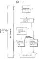
- Fig. 1 is a schematic block diagram useful for understanding an embodiment of the data processing system in a loosely coupled pipeline processor according to the present invention;
- Fig. 2 is a detailed diagram for the description of a part of the diagram of Fig. 1;
- Fig. 3 is a timing chart useful for understanding the operation of the system illustrated in Figs. 1 and 2;
- Fig. 4 is a schematic block diagram useful for understanding a second embodiment of the data processing system in the loosely coupled pipeline processor according to the present invention;
- Fig. 5 is a detailed diagram for the description of a part of the diagram of Fig. 4;
- Fig. 6 is a detailed diagram useful for understanding a third embodiment of the data processing system in the loosely coupled pipeline processor according to the present invention;
- Fig. 7 is a detailed diagram useful for understanding a fourth embodiment of the data processing system in the loosely coupled pipeline processor according to the present invention;
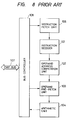
- Fig. 8 is a schematic block diagram useful for understanding a conventional data processing system in a conventional pipeline processor; and
- Fig. 9 is a timing chart useful for understanding the operation of the system illustrated in Fig. 8.
- The same or corresponding elements and parts are designated at like reference numerals throughout the drawings.
- Prior to describing the embodiments of the present invention, a conventional method will be discussed first for a better understanding of the present invention.
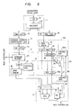
- Fig. 8 illustrates one example of a conventional data processing method. A conventional pipeline processor comprises an
instruction decoder 101, an operandaddress computation unit 102, an operand pre-fetchunit 103, anarithmetic unit 104, aninstruction fetch unit 106, achip bus 107, and abus controller 108. In theinstruction decoder 101, an instruction code fetched at theinstruction fetch unit 106 is decoded. Then, control information relating to instruction execution is generated at theinstruction decoder 101, and is sent to the operandaddress computation unit 102. When the fetch of an operand in memory is required, control information for an operand address computation and control information for a memory access are also sent to the operandaddress computation unit 102. Besides, if the writing into the memory is required, control information for an operand address computation is sent to the operandaddress computation unit 102. In the operandaddress computation unit 102, a required operand address thereof is computed and is sent to the operand pre-fetchunit 103, and control information for a memory access and the control information relating to the instruction execution are also sent to the operand pre-fetchunit 103. In the operand pre-fetchunit 103, a memory operand is accessed via thebus controller 108 and thechip bus 107, and the reading out of the memory operand is performed in accordance with the operand address sent from the operandaddress computation unit 102. Then, the read out operand data, the address for the writing into the memory, and the control information relating to the instruction execution are sent to thearithmetic unit 104. In thearithmetic unit 104, an operation is executed in accordance with the read out operand data sent from the operand pre-fetchunit 103 and the control information relating to the instruction execution. If the writing into the memory is required, the result of the operation is written into the memory via thebus controller 108 and thechip bus 107 in accordance with the writing address sent from the operand pre-fetchunit 103. - The operation of the conventional pipeline processor having the above-mentioned structure will be described hereinbellow with reference to Fig. 9.
- Fig. 9 illustrates a timing chart of the operation of the conventional pipeline processor of Fig. 8. In Fig. 9, the number of clock pulses in each unit is assumed as follows: one clock for the
instruction decoder 101, one clock (pulse) for the operandaddress computation unit 102, three clocks for the operand pre-fetchunit 103, and one clock for thearithmetic unit 104. It is also assumed that the executing instruction sequence consists of three instructions, i.e. one instruction in which fetching a memory operand and two instructions in which fetching the same. Namely, instructions (1), (4), and (7) require the fetch of a memory operand, and instructions (2), (3), (5), (6), (8), and (9) do not require the fetch thereof. Moreover, it is assumed that the begining state on the pipeline process is an initialized state, for example, a state just after the execution of a branch instruction. - The instruction (1) is decoded in the
instruction decoder 101 in the time period of clock t1, and the control information relating to the instruction execution and the control information for the memory access and operand address computation are sent to the operandaddress computation unit 102. In clock t2, the operand address is computed in the operandaddress computation unit 102 in accordance with the control information for the memory access and operand address computation. The operand address, the control information relating to the instruction execution, and the control information for the memory access are also sent to the operand pre-fetchunit 103. While clocks t3-t5, the memory operand is read out in the operand pre-fetchunit 103 in accordance with the control information for the address computation and memory access, and the control information for the memory access and the control information relating to the instruction execution are sent to thearithmetic unit 104. In clock t6, the operation is executed in thearithmetic unit 104 in accordance with the control information relating to the instruction execution. - The instruction (2) is decoded in the
instruction decoder 101 in the clock t2, only control information relating to the execution of the instruction (2) is sent to the operandaddress computation unit 102 because the instruction (2) does not require the fetch of the memory operand. In the clock t3, although this instruction (2) is passed through the operandaddress computation unit 102 as a pipeline stage, since there are no control information for the address computation and memory access, the control information relating to the execution of the instruction (2) is sent to theoperand pre-fetch unit 103. However, since the execution of the instruction (1) in theoperand pre-fetch unit 103 is not completed, the sending of the control information relating to the execution of the instruction (2) is actually delayed until clock t6. In the clock t6, although the instruction (2) is also passed through theoperand pre-fetch unit 103 as a pipeline stage, since there is no control information for the operand address computation and memory access, only the control information for the execution of the instruction (2) is sent to thearithmetic unit 104. In clock t7, the operation is executed in thearithmetic unit 104 in accordance with the control information for the execution of the instruction (2). Such pipeline process is continued as shown in Fig. 9. - However, the above-mentioned pipeline process brings about the following disadvantage. The transmission of unnecessary information in instructions is required even when an instruction relates to the operation of registers, where the fetch of a memory operand is not required. Therefore, such unnecessary passing of the information brings about a limitation of bus band width used for operand access in a block of instruction that the fetch of a memory operand is required. As will be seen from Fig. 9, assuming that the ratio of the number of instructions in which the fetch of memory operand is required to the number of instructions in which the fetch of the same is not required is 1:2, and that the ratio of an executing time for fetching the same to an excecuting time for non-fetching is 3:1, the using of the bus band. width is limitted to 60%.
- Fig. 1 illustrates a schematic block diagram showing an embodiment of the data processing system of a loosely coupled pipeline processor according to the present invention. The loosely coupled pipeline processor comprises an
instruction decoder 1 for decoding instructions, an operandaddress computation unit 2 for computing the address of an operand, anoperand pre-fetch unit 3 for previously fetching an operand, anarithmetic unit 4 for executing operations, acontrol information buffer 5, an instruction fetchunit 6 for fetching instructions, achip bus 7, and abus controller 8. In theinstruction decoder 1, an instruction code accepted at the instruction fetchunit 6 is decoded. Then, control information for an address computation is sent to the operandaddress computation unit 2, and control information for instruction execution is sent to thecontrol information buffer 5. In the operandaddress computation unit 2, the address of an operand is computed, and control information for memory access is sent to theoperand pre-fetch unit 3. In theoperand pre-fetch unit 3, operand data in a memory is accessed via thebus controller 8 and thechip bus 7, and an operandready signal 9 is sent to thecontrol information buffer 5. In thecontrol information buffer 5, the control information sent from theinstruction decoder 1 is queued, and is sent to thearithmetic unit 4 in accordance with a request signal from thearithmetic unit 4. The above is a brief description of the operation of the system of Fig. 1. - Fig. 2 is a detailed diagram for the description of a part of the block diagram of Fig. 1. The
instruction decoder 1 comprises an instruction register (IR) 10 and adecoder 11. In theinstruction decoder 1, an instruction code read out in the instruction fetchunit 6 is stored into theIR 10, and decoded by thedecoder 11. When the fetch of a memory operand is required, controlinformation 12 for an address computation and a memory access is sent to the operandaddress computation unit 2 and controlinformation 13 for instruction execution is sent to thecontrol information buffer 5. Thecontrol information 12 comprises information (OAG) for operand address computation and information (ACS) for a memory access. When the fetch of an operand in the memory is not required, only thecontrol information 13 is sent to thecontrol information buffer 5. Thecontrol information 13 comprises information (OP) showing the kind of operation, information (SRC) designating a source operand, information (DST) showing a destination operand, and information (MEM) showing whether an operand in the memory is required or not. - In the operand
address computation unit 2, the address of the operand is computed in accordance with the information OAG in thecontrol information 12, and controlinformation 14 is sent to theoperand pre-fetch unit 3. Thecontrol information 14 comprises an operand address (OA) and the information ACS. - The
operand pre-fetch unit 3 comprises anoperand reader 20, adata queue portion 15, and acontrol unit 21. In theoperand pre-fetch unit 3, if the fetch of an operand in memory is required, theoperand reader 20 outputs a request signal (not shown) to thebus control unit 8. Then, the memory operand is read out in accordance with the operand address OA and the information ACS in thecontrol information 14 sent from the operandaddress computation unit 2, and such read out memory operand data (OD) is queued in thedata queue portion 15. The data OD is sent to thearithmetic unit 4 as an input data for executing an operation. Thecontrol unit 21 referres to the status of thedata queue portion 15, and outputs the operandready signal 9 to thecontrol information buffer 5 when at least one operand datum OD exists in thedata queue portion 15. - The
control information buffer 5 comprises adata queue portion 30 for the information OP, SRC, and DST, adata queue portion 31 for the information MEM, acontrol unit 32 for controlling the sending of the information in thedata queue portion 30, and a synchronizing circuit means 33. In thecontrol information buffer 5, the information OP, SRC, and DST in thecontrol information 13 sent from theinstruction decoder 1 is queued in thedata queue portion 30, and the information MEM in thecontrol information 13 is queued in thedata queue portion 31. Thecontrol unit 32 outputs asignal 34 to the synchronizing circuit means 33 when the information OP, SRC, and DST, i.e.information 16 is queued in thedata queue portion 30, and sends theinformation 16 to thearithmetic unit 4 when receiving therequest signal 50 from thearithmetic unit 4. The synchronizing circuit means 33 generates an enablingsignal 17 representing that theinformation 16 is valid in accordance with the operandready signal 9, the information MEM sent from thedata queue portion 31, and the signal from thecontrol unit 32. - Thus,
information 16 in thecontrol information 13 is sent to thearithmetic unit 4 in accordance with arequest signal 50 fed therefrom. Namely, if theinformation 16 needs the fetch of memory operand data, it is required that the status of thedata queue portion 15 is considered. In other words, whether the operandready signal 9 is outputted or not is referred by the synchronising circuit means 33. If the operandready signal 9 is not sent from theoperand pre-fetch unit 3, i.e. if there is no read out operand datum in thedata queue portion 15, the transmission of theinformation 16 is delayed. It is to be noted that when the enablingsignal 17 is invalid, thearithmetic unit 4 does not send therequest signal 50 to thecontrol information buffer 5. More specifically, when the information MEM indicates that an operand in memory has to be fetched, and when the operandready signal 9 is not sent, thecontrol information 16 is in invalid state. Therefore, the sending of theinformation 16 is delayed until the operandready signal 9 is sent to thecontrol information buffer 5. - The
arithmetic unit 4 comprises an arithmetic logic unit (ALU) 40, aregister bank 18 having a plurality of general (purpose) registers, and acontrol unit 42. In thearithmetic unit 4, thecontrol unit 42 outputs therequest signal 50 to thecontrol unit 32 in thecontrol information buffer 5 in accordance with the enablingsignal 17 sent from thecontrol information buffer 5. It is to be noted that the transmission of theinformation 16 can be performed by a handshake control. In this case, therequest signal 50 can be outputted before the enablingsignal 17 is recieved in thecontrol unit 42. When executing operation in accordance with theinformation 16 and the enablingsignal 17, if the information SRC and the information DST in theinformation 16 shows a general register number, its data is read out from its general register in theregister bank 18, and the operation is performed in accordance with the information OP. Then, the result of the operation is stored in the general register where the information DST shows. If the information SRC or the information DST shows the memory operand, the data OD sent from theoperand pre-fetch unit 3 is used as input data of theALU 40. In addition, if the information DST shows the memory operand, it is performed that the result of its operation is written into the memory via thebus control unit 8. - The actual operation of the loosely coupled pipeline processor having the above-mentioned structure of Fig. 1 and Fig. 2 according to the present invention will be described hereinbelow with reference to Fig. 3 showing a timing chart associated with an embodiment of the present invention.
- In Fig. 3, instructions executed in the
instruction decoder 1, the operandaddress computation unit 2, theoperand pre-fetch unit 3, and thearithmetic unit 4, and the resulted queueing status in thedata queue portion 30 of thecontrol information buffer 5 are shown by the unit of a clock. It is assumed that the required number of the clock pulses in each unit for pipeline process is as follows: one clock for theinstruction decoder 1, one clock for the operandaddress computation unit 2, three clocks for theoperand pre-fetch unit 3, and one clock for thearithmetic unit 4. It is also assumed that executing instruction sequence consists of three instructions, i.e. one instruction that the fetch of a memory operand is required and two instructions that the fetch is not required. Namely, instructions (1), (4), (7), (10), and (13) require the fetch of a memory operand, and instructions (2), (3), (5), (6), (8), (9), (11), (12), (14), and (15) do not require the fetch thereof. Moreover, it is assumed that the begining state of the pipeline process is an initialized state, e.g. a state just after the execution of a branch instruction. - The instruction (1) is decoded in the
instruction decoder 1 in a clock t1, and controlinformation 12 is sent to the operandaddress computation unit 2, as well ascontrol information 13 is sent to thecontrol information buffer 5. However, since the operandready signal 9 is not ready in thecontrol information buffer 5, controlinformation 16 is held in thecontrol information buffer 5. Thus, the transmission of thecontrol information 16 is delayed. In clock t2, an operand address is computed in the operandaddress computation unit 2 in accordance with thecontrol information 12. While clocks t3-t5, the operand is read out in theoperand pre-fetch unit 3, and the operandready signal 9 is sent to thecontrol information buffer 5. Then, thecontrol information 16 being stored in thedata queue portion 30 of thecontrol information buffer 5 is sent to thearithmetic unit 4. In clock t6, the operation is executed in thearithmetic unit 4 in accordance with thecontrol information 16. - The instruction (2) is decoded in the
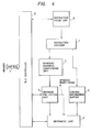
instruction decoder 1 during the clock t2, and then only controlinformation 13 according to the instruction (2) is sent to thecontrol information buffer 5 because the instruction (2) does not need the fetch of the memory operand. However, since the sending of the operandready signal 9 is not completed yet, controlinformation 16 according to the instruction (2) is held in thedata queue portion 30. The sending of thiscontrol information 16 is delayed until clock t7. In this embodiment, theoperand pre-fetch unit 3 acts as a control factor, or a velocity controlling step, and therefore 100% of the bus band width is used for the operand access as shown in Fig. 3. - Fig. 4 illustrates the structure of the second embodiment of loosely coupled pipeline processors according to the present invention. In Fig. 5, elements, except for a control information buffer 5A, and an arithmetic unit 4A, designated at the same reference numerals as in Fig. 1 respectively have the same function as those in Fig. 1. The operand
ready signal 9 is not sent to the control information buffer 5A but is sent to the arithmetic unit 4A. The control information buffer 5A and the arithmetic unit 4A will be described with reference to Fig. 5. - Fig. 5 illustrates a detailed diagram of Fig. 4. In Fig. 5, the control information buffer 5A comprises
data queue portions control unit 32, and the arithmetic unit 4A comprisesALU 40,register bank 18, synchronizing circuit means 33, and a control unit 42A. Since the arithmetic unit 4A has the synchronizing circuit means 33, the operandready signal 9 is sent to the arithmetic unit 4A. Thecontrol unit 32 sendssignal 34 representing thatinformation 16 has been queued indata queue portion 30 to the control unit 42A. When the control unit 42A acceptssignal 34 outputted fromcontrol unit 32, asignal 19 representing that thesignal 34 has been received is outputted to the synchronizing circuit means 33. The synchronizing circuit means 33 outputs the enablingsignal 17 to the control unit 42A in accordance with the operandready signal 9, the information MEM sent from the control information buffer 5A, and thesignal 19. Then, therequest signal 50 is outputted to thecontrol unit 32 for accepting the information signal 16 from the control information buffer 5A. Thus, an operation is executed at the arithmetic unit 4A. - Fig. 6 is a detailed diagram useful for understanding a third embodiment of the data processing system in the loosely coupled pipeline processor according to the present invention. In Fig. 6, the
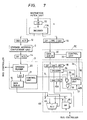
instruction decoder 11 comprisesinstruction register 10 and adecoder 11A, and acontrol information buffer 5B comprisesdata queue portion 30, adecoder 36, synchronizing circuit means 33, and acontrol unit 32A. Thedecoder 11A sends only theinformation 16 to thecontrol information buffer 5B. If theinformation 16 is queued in thedata queue 30, since thedecoder 36 can read theinformation 16A having SRC and DST, theinformation 16A can be decoded for generating asignal 35 representing that the information SRC and/or DST require the memory operand. Then thesignal 35 is sent to the synchronizing circuit means 33, and operates as the information MEM in Fig. 2. Thedecoder 36 also sends theinformation 16A to thearithmetic unit 4 when thecontrol unit 32A recieves therequest signal 50 from thearithmetic unit 4. At this time, theinformation 16A may not pass through thedecoder 36. - Fig. 7 is a detailed diagram useful for understanding a fourth embodiment of the data processing system in the loosely coupled pipeline processor according to the present invention. In Fig. 7, a
control information buffer 5C comprisesdata queue portion 30 and contol unit 32B, andarithmetic unit 4B comprisesdecoder 36, synchronizing circuit means 33, a control unit 42C,ALU 40, and registerbank 18. When thecontrol unit 42B recieves the enablingsignal 17, theinformation 16 is sent to thearithmetic unit 30. At this time, theinformation 16A may send from thedecoder 36 to the register bank. - As will be seen from the above description of the present invention, the
control information 12 for controlling the operandaddress computation unit 2 and theoperand pre-fetch unit 3 and thecontrol information 13 for controlling thearithmetic unit 4 are separately outputted from theinstruction decoder 1. Thecontrol information 13 is queued to thecontrol information buffer 5, and the information OP, SRC, and DST are sent to thearithmetic unit 4 in accordance with therequest signal 50 from thearithmetic unit 4. It is to be noted that the transmission of theinformation 16 can be performed by a handshake control. In this case, therequest signal 50 can be outputted before the enablingsignal 17 is recieved in the control unit of the arithmetic unit. Thus, a process relating to the fetch of an operand is independent as a secondary pipeline stage from the main pipeline stage comprising steps of an instruction fetch, an instruction decoding, and an instruction execution. When the instruction does not contain a process of the fetch of the memory operand, e.g. the instruction execution of an operation between registers, only the main pipeline stage is acted. Therefore, control information (13) in an instruction that the fetch of the memory operand is not required does not pass through the pipeline stage relating to the fetch of the memory operand thereby improving the bus band width. As a result, overhead, required for filling of pipeline processes just after the execution of a branch instruction, is avoidable. Moreover, in these embodiments, since theoperand pre-fetch unit 3 has a queueing function, the method of the pipeline process according to the present invention is adaptable even if the ratio of the number of instructions in which the fetch of memory operand is required to the number of instructions in which the fetch of the same is not required is partly changed. - From the foregoing, it will be understood that effective pipeline process can be actualized by using a loosely coupled pipeline processor of the present invention.
- In the above-mentioned embodiments, an address converting unit may be provided to the
operand pre-fetch unit 3, the instruction fetchunit 6, or thebus controller 8 when the present invention is applied to a virtual memory technique. Besides, a cache memory may also be provided to theoperand pre-fetch unit 3, the instruction fetchunit 6, or thebus controller 8 when a cache memory technique is applied to the present invention. Particularly, if a data cache memory is provided to theoperand pre-fetch unit 3, the number of the required clock pulses in theoperand pre-fetch unit 3 can considerablly be reduced. In addition, the operandaddress computation unit 2 and theoperand pre-fetch unit 3 may be combined each other as one unit, and each unit may comprise a plurality of pipeline stages.
Claims (17)
- A central processing unit having an instruction fetch unit (6) for fetching an instruction, an instruction decoder (1) for decoding the instruction fetched by the instruction fetch unit, for generating and outputting first control information (16; or OP) relating to execution for the instruction and for generating and outputting second control information (ACS) for a memory access and third control information (OAG) far an operand address computation in case where a fetching of an operand in a memory is required for execution of the decoded instruction, an operand address computation unit (2) for receiving the second control information and the third control information, for computing an operand address in accordance with the third control information and for outputting the computed operand address, an operand pre-fetch unit (3) for receiving the computed operand address and the second control information from the operand address computation unit, for fetching a memory operand in accordance with the received operand address and for outputting the fetched memory operand and an operation unit (4 and 5; 4' and 5'; 4 and 5B; 4B and 5C) for receiving the first control information in case where a fetching of an operand in a memory is not required for execution of the decoded instruction, for receiving the memory operand from the operand pre-fetch unit and also receiving the first control information in case where a fetching of an operand in a memory is required for execution of the decoded instruction, and for executing an operation in accordance with the first control information in case where a fetching of an operand in a memory is not required for execution of the decoded instruction, and in accordance with the memory operand and the first control information in case where a fetching of an operand in a memory is required, the central processing unit, characterized in that
the operand pre-fetch unit queues the fetched memory operand and outputs said memory operand and a first signal (9) representing that the memory operand has been queued therein,
the operation unit comprises a control information buffer (5; 5'; 5B; 5C) for queuing and outputting the first control information, and for outputting a second signal (17 or 34) for causing a request to output the first control information and an arithmetic unit (4; 4'; 4B) for receiving the second signal and for outputting a third signal (50) representing that the arithmetic unit requires the first control information queued in the control information buffer,
the control information buffer receives the first control information from the instruction decoder,
the control information buffer outputs the first control information to the arithmetic unit in response to the third signal and
when an operand in the memory is required, and when the first signal is not sent to the operation unit, an outputting of the first control signal from the control information buffer is delayed until the first signal is sent to the operation unit. - The central processing unit as claimed in Claim 1, characterized in that the instruction decoder further generates fourth control information (MEM) indicating whether or not an operand in the memory is required,
fifth control information (SRC) designating a source operand and sixth information (DST) representing a destination operand, wherein the first signal is sent to the control information buffer, wherein the control information buffer outputs the second signal, which is a signal (17) representing that the first control information, the fifth control information and the sixth information are valid in accordance with the first signal and the fourth control information. - The central processing unit as claimed in Claim 2, characterized in that the operand pre-fetch unit includes:(i) an operand reader (20) for reading the memory operand;(ii) a first storage means (15) for queuing the memory operand to send the memory operand to the arithmetic unit; and(iii) a first control unit (21) for sending the first signal to the control information buffer when the memory operand is queued in the first storage means.
- The central processing unit as claimed in Claim 2, characterized in that the control information buffer (5) includes:(i) a second storage means (30) for queuing the first control information to send the first control information to the arithmetic unit (4);(ii) a third storage means (31) for queuing and outputting the fourth control information;(iii) a second control unit (32) for outputting a fourth signal (34) indicating that the first control information has been queued in the second storage means, and for receiving the third signal; and(iv) a synchronizing circuit means (33) responsive to the first and fourth signals and the fourth control information from the third storage means for outputting the second signal.
- The central processing unit as claimed in Claim 2, characterized in that the arithmetic unit (4) includes:(i) an arithmetic logic unit (40)(ii) a register bank (18) having general purpose registers; and(iii) a third control unit (42) for receiving the second signal and for outputting the third signal to the control information buffer.
- The central processing unit as claimed in Claim 1, characterized in that the second signal is a signal (34) representing that the first control information has been queued in the control information buffer, and wherein the first signal is sent to the arithmetic unit.
- The central processing unit as claimed in Claim 6, characterized in that the operand pre-fetch unit includes:(i) an operand reader (20) for reading the memory operand;(ii) a first storage means (15) for queuing the memory operand to send the memory operand to the arithmetic unit; and(iii) a first control unit (21) for sending the first signal to the control information buffer when the memory operand is queued in the first storage means.
- The central processing unit as claimed in Claim 6, characterized in that the control information buffer (5') includes:(i) a second storage means (30) for queuing the first control information to send the first control information to the arithmetic unit (4');(ii) a third storage means (31) for queuing and outputting the fourth control information; and(iii) a second control unit (32) for outputting the second signal (34) indicating that the first control information has been queued in the second storage means, and for receiving the third signal.
- The central processing unit as claimed in Claim 6, characterized in that the instruction decoder further generates fourth control information (MEM) indicating whether or not an operand in the memory is required, wherein the control information buffer receives the fourth control information from the instruction decoder, and
wherein the arithmetic unit (4') includes:(i) an arithmetic logic unit (40)(ii) a register bank (18) having general purpose registers; and(iii) a third control unit (42') for receiving the second signal, for outputting the third signal to the control information buffer (5'), for outputting a fourth signal (19) representing that the second signal has been received and for receiving a fifth signal (17) representing that the first control information is valid in accordance with the first signal and the fourth control information; and(iv) a synchronizing circuit means (33) responsive to the first and second signals and the fourth control information from the control information buffer for outputting the fifth signal. - The central processing unit as claimed in Claim 1, characterized in that the instruction decoder further generates fourth control information (SRC + DST) indicating a source operand and a destination operand, wherein the first signal is sent to the control information buffer (5B), wherein the control information buffer generates a fourth signal (35) by decoding the fourth control information and outputs the second signal, which is the signal (17) representing that the first control information and the fourth control information are valid in accordance with the first signal and the fourth signal (35), and wherein the fourth signal indicates whether or not an operand in the memory is required.
- The central processing unit as claimed in Claim 10, characterized in that the operand pre-fetch unit includes:(i) an operand reader (20) for reading the memory operand;(ii) a first storage means (15) for queuing the memory operand to send the memory operand to the arithmetic unit; and(iii) a first control unit (21) for sending the first signal to the control information buffer when the memory operand is queued in the first storage means.
- The central processing unit as claimed in Claim 10, characterized in that the control information buffer (5B) includes:(i) a second storage means (30) for queuing the first control information and the fourth control information to send the first control information and the fourth control information to the arithmetic unit (4);(ii) a second control unit (32A) for outputting a fifth signal (34) indicating that the first control information and the fourth control information have been queued in the second storage means, and for receiving the third signal;(iii) a decoder (36) for decoding the fourth control information thereby outputting the fourth signal (35); and(iv) a synchronizing circuit means (33) responsive to the first, fourth and fifth signals for outputting the second signal.
- The central processing unit as claimed in Claim 10, characterized in that the arithmetic unit (4) includes:(i) an arithmetic logic unit (40)(ii) a register bank (18) having general purpose registers; and(iii) a third control unit (42) for receiving the second signal and for outputting the third signal to the control information buffer.
- The central processing unit as claimed in Claim 1, characterized in that the instruction decoder further generates fourth control information (SRC + DST) indicating a source operand and a destination operand, wherein the first signal is sent to the arithmetic unit (4B), wherein the control information buffer (5C) outputs the second signal, which is a signal (34) representing that the first control information and the fourth control information have been queued, and wherein the arithmetic unit generates a fourth signal (35) by decoding the fourth control information and wherein the fourth signal indicates whether or not an operand in the memory is required.
- The central processing unit as claimed in Claim 14, characterized in that the operand pre-fetch unit includes:(i) an operand reader (20) for reading the memory operand;(ii) a first storage means (15) for queuing the memory operand to send the memory operand to the arithmetic unit; and(iii) a first control unit (21) for sending the first signal to the control information buffer when the memory operand is queued in the first storage means.
- The central processing unit as claimed in Claim 14, characterized in that the control information buffer (5C) includes:(i) a second storage means (30) for queuing the first control information and the fourth control information to send the first control information and the fourth control information to the arithmetic unit (4B); and(ii) a second control unit (32) for outputting the second signal (34), and for receiving the third signal.
- The central processing unit as claimed in Claim 14, characterized in that the arithmetic unit (4B) includes:(i) an arithmetic logic unit (40)(ii) a register bank (18) having general purpose registers;(iii) a decoder (36) for decoding the fourth control information thereby outputting the fourth signal (35);(iv) a third control unit (42B) for receiving the second signal, for outputting a fifth signal (19) representing that the second signal has been received and for outputting the third signal to the control information buffer; and(v) a synchronizing circuit means (33) responsive to the first, fourth and fifth signals for outputting a sixth signal (17) representing that the first control information and the fourth control information are valid in accordance with the first signal, the fourth signal and the fifth signal, and wherein the third control unit inputs the sixth signal generated by the synchronizing circuit.
Applications Claiming Priority (2)
| Application Number | Priority Date | Filing Date | Title |
|---|---|---|---|
| JP61311023A JP2695157B2 (en) | 1986-12-29 | 1986-12-29 | Variable pipeline processor |
| JP311023/86 | 1986-12-29 |
Publications (3)
| Publication Number | Publication Date |
|---|---|
| EP0272705A2 EP0272705A2 (en) | 1988-06-29 |
| EP0272705A3 EP0272705A3 (en) | 1990-12-19 |
| EP0272705B1 true EP0272705B1 (en) | 1994-06-08 |
Family
ID=18012186
Family Applications (1)
| Application Number | Title | Priority Date | Filing Date |
|---|---|---|---|
| EP87119276A Expired - Lifetime EP0272705B1 (en) | 1986-12-29 | 1987-12-28 | Loosely coupled pipeline processor |
Country Status (5)
| Country | Link |
|---|---|
| US (1) | US4967338A (en) |
| EP (1) | EP0272705B1 (en) |
| JP (1) | JP2695157B2 (en) |
| KR (1) | KR910006144B1 (en) |
| DE (1) | DE3750028T2 (en) |
Cited By (6)
| Publication number | Priority date | Publication date | Assignee | Title |
|---|---|---|---|---|
| US6061749A (en) | 1997-04-30 | 2000-05-09 | Canon Kabushiki Kaisha | Transformation of a first dataword received from a FIFO into an input register and subsequent dataword from the FIFO into a normalized output dataword |
| US6118724A (en) | 1997-04-30 | 2000-09-12 | Canon Kabushiki Kaisha | Memory controller architecture |
| US6195674B1 (en) | 1997-04-30 | 2001-02-27 | Canon Kabushiki Kaisha | Fast DCT apparatus |
| US6311258B1 (en) | 1997-04-03 | 2001-10-30 | Canon Kabushiki Kaisha | Data buffer apparatus and method for storing graphical data using data encoders and decoders |
| US6336180B1 (en) | 1997-04-30 | 2002-01-01 | Canon Kabushiki Kaisha | Method, apparatus and system for managing virtual memory with virtual-physical mapping |
| US6707463B1 (en) | 1997-04-30 | 2004-03-16 | Canon Kabushiki Kaisha | Data normalization technique |
Families Citing this family (16)
| Publication number | Priority date | Publication date | Assignee | Title |
|---|---|---|---|---|
| IL92605A0 (en) * | 1988-12-19 | 1990-08-31 | Bull Hn Information Syst | Production line method and apparatus for high performance instruction execution |
| US5109495A (en) * | 1989-02-03 | 1992-04-28 | Digital Equipment Corp. | Method and apparatus using a source operand list and a source operand pointer queue between the execution unit and the instruction decoding and operand processing units of a pipelined data processor |
| JP2538053B2 (en) * | 1989-05-08 | 1996-09-25 | 松下電器産業株式会社 | Control device |
| US5150468A (en) * | 1989-06-30 | 1992-09-22 | Bull Hn Information Systems Inc. | State controlled instruction logic management apparatus included in a pipelined processing unit |
| JPH04260929A (en) * | 1991-01-21 | 1992-09-16 | Mitsubishi Electric Corp | Data processor |
| JPH04340145A (en) * | 1991-05-17 | 1992-11-26 | Nec Corp | Cache memory device |
| US5546593A (en) * | 1992-05-18 | 1996-08-13 | Matsushita Electric Industrial Co., Ltd. | Multistream instruction processor able to reduce interlocks by having a wait state for an instruction stream |
| US6240508B1 (en) * | 1992-07-06 | 2001-05-29 | Compaq Computer Corporation | Decode and execution synchronized pipeline processing using decode generated memory read queue with stop entry to allow execution generated memory read |
| US5706459A (en) * | 1994-01-06 | 1998-01-06 | Fujitsu Limited | Processor having a variable number of stages in a pipeline |
| AUPO648397A0 (en) * | 1997-04-30 | 1997-05-22 | Canon Information Systems Research Australia Pty Ltd | Improvements in multiprocessor architecture operation |
| JP2944563B2 (en) * | 1997-04-03 | 1999-09-06 | 甲府日本電気株式会社 | Pipeline type information processing device |
| US6061755A (en) * | 1997-04-14 | 2000-05-09 | International Business Machines Corporation | Method of layering cache and architectural specific functions to promote operation symmetry |
| US5978871A (en) * | 1997-04-14 | 1999-11-02 | International Business Machines Corporation | Method of layering cache and architectural specific functions for operation splitting |
| US6272616B1 (en) * | 1998-06-17 | 2001-08-07 | Agere Systems Guardian Corp. | Method and apparatus for executing multiple instruction streams in a digital processor with multiple data paths |
| US20050240806A1 (en) * | 2004-03-30 | 2005-10-27 | Hewlett-Packard Development Company, L.P. | Diagnostic memory dump method in a redundant processor |
| CN102681796B (en) * | 2012-05-18 | 2015-04-08 | 重庆大学 | RAM (Random Access Memory) distribution structure in data multistage pipelining algorithm module |
Citations (1)
| Publication number | Priority date | Publication date | Assignee | Title |
|---|---|---|---|---|
| EP0184791A1 (en) * | 1984-12-07 | 1986-06-18 | Nec Corporation | Information processing device capable of rapidly processing instructions of different groups |
Family Cites Families (9)
| Publication number | Priority date | Publication date | Assignee | Title |
|---|---|---|---|---|
| US4342078A (en) * | 1979-05-21 | 1982-07-27 | Motorola, Inc. | Instruction register sequence decoder for microprogrammed data processor and method |
| JPS57155666A (en) * | 1981-03-20 | 1982-09-25 | Fujitsu Ltd | Instruction controlling system of vector processor |
| US4541045A (en) * | 1981-09-21 | 1985-09-10 | Racal-Milgo, Inc. | Microprocessor architecture employing efficient operand and instruction addressing |
| JPS5890247A (en) * | 1981-11-25 | 1983-05-28 | Nippon Telegr & Teleph Corp <Ntt> | Pipeline controlling system of information processor |
| US4597041A (en) * | 1982-11-15 | 1986-06-24 | Data General Corp. | Method and apparatus for enhancing the operation of a data processing system |
| WO1985000453A1 (en) * | 1983-07-11 | 1985-01-31 | Prime Computer, Inc. | Data processing system |
| JPS60129837A (en) * | 1983-12-19 | 1985-07-11 | Matsushita Electric Ind Co Ltd | Signal processing operation processor |
| JPS60186936A (en) * | 1984-03-05 | 1985-09-24 | Hitachi Ltd | Programmable controller |
| IT1275935B1 (en) * | 1995-03-17 | 1997-10-24 | Chiesi Farma Spa | AMINOTETRALINE DERIVATIVES FOR THERAPY OF CARDIOVASCULAR DISEASES |
-
1986
- 1986-12-29 JP JP61311023A patent/JP2695157B2/en not_active Expired - Fee Related
-
1987
- 1987-12-28 EP EP87119276A patent/EP0272705B1/en not_active Expired - Lifetime
- 1987-12-28 DE DE3750028T patent/DE3750028T2/en not_active Expired - Fee Related
- 1987-12-28 US US07/137,923 patent/US4967338A/en not_active Expired - Lifetime
- 1987-12-29 KR KR1019870015245A patent/KR910006144B1/en not_active IP Right Cessation
Patent Citations (1)
| Publication number | Priority date | Publication date | Assignee | Title |
|---|---|---|---|---|
| EP0184791A1 (en) * | 1984-12-07 | 1986-06-18 | Nec Corporation | Information processing device capable of rapidly processing instructions of different groups |
Cited By (14)
| Publication number | Priority date | Publication date | Assignee | Title |
|---|---|---|---|---|
| US6393545B1 (en) | 1919-04-30 | 2002-05-21 | Canon Kabushiki Kaisha | Method apparatus and system for managing virtual memory with virtual-physical mapping |
| US6311258B1 (en) | 1997-04-03 | 2001-10-30 | Canon Kabushiki Kaisha | Data buffer apparatus and method for storing graphical data using data encoders and decoders |
| US6195674B1 (en) | 1997-04-30 | 2001-02-27 | Canon Kabushiki Kaisha | Fast DCT apparatus |
| US6246396B1 (en) | 1997-04-30 | 2001-06-12 | Canon Kabushiki Kaisha | Cached color conversion method and apparatus |
| US6259456B1 (en) | 1997-04-30 | 2001-07-10 | Canon Kabushiki Kaisha | Data normalization techniques |
| US6272257B1 (en) | 1997-04-30 | 2001-08-07 | Canon Kabushiki Kaisha | Decoder of variable length codes |
| US6061749A (en) | 1997-04-30 | 2000-05-09 | Canon Kabushiki Kaisha | Transformation of a first dataword received from a FIFO into an input register and subsequent dataword from the FIFO into a normalized output dataword |
| US6336180B1 (en) | 1997-04-30 | 2002-01-01 | Canon Kabushiki Kaisha | Method, apparatus and system for managing virtual memory with virtual-physical mapping |
| US6349379B2 (en) | 1997-04-30 | 2002-02-19 | Canon Kabushiki Kaisha | System for executing instructions having flag for indicating direct or indirect specification of a length of operand data |
| US6118724A (en) | 1997-04-30 | 2000-09-12 | Canon Kabushiki Kaisha | Memory controller architecture |
| US6414687B1 (en) | 1997-04-30 | 2002-07-02 | Canon Kabushiki Kaisha | Register setting-micro programming system |
| US6507898B1 (en) | 1997-04-30 | 2003-01-14 | Canon Kabushiki Kaisha | Reconfigurable data cache controller |
| US6674536B2 (en) | 1997-04-30 | 2004-01-06 | Canon Kabushiki Kaisha | Multi-instruction stream processor |
| US6707463B1 (en) | 1997-04-30 | 2004-03-16 | Canon Kabushiki Kaisha | Data normalization technique |
Also Published As
| Publication number | Publication date |
|---|---|
| EP0272705A3 (en) | 1990-12-19 |
| KR880008150A (en) | 1988-08-30 |
| JPS63167935A (en) | 1988-07-12 |
| JP2695157B2 (en) | 1997-12-24 |
| US4967338A (en) | 1990-10-30 |
| EP0272705A2 (en) | 1988-06-29 |
| DE3750028D1 (en) | 1994-07-14 |
| DE3750028T2 (en) | 1994-10-06 |
| KR910006144B1 (en) | 1991-08-16 |
Similar Documents
| Publication | Publication Date | Title |
|---|---|---|
| EP0272705B1 (en) | Loosely coupled pipeline processor | |
| EP0220682B1 (en) | Data processing system | |
| EP0287115B1 (en) | Coprocessor and method of controlling the same | |
| EP0363889B1 (en) | Vector processor using buffer for preparing vector data | |
| US5088030A (en) | Branch address calculating system for branch instructions | |
| EP0223150B1 (en) | Information processing apparatus | |
| US4677549A (en) | Pipelined data processor system having increased processing speed | |
| EP0354740A2 (en) | Data processing apparatus for performing parallel decoding and parallel execution of a variable word length instruction | |
| EP0240606B1 (en) | Pipe-line processing system and microprocessor using the system | |
| EP0079370B1 (en) | Digital computer for executing instructions in three time-multiplexed portions | |
| US5276822A (en) | System with enhanced execution of address-conflicting instructions using immediate data latch for holding immediate data of a preceding instruction | |
| EP0324952B1 (en) | Branching circuit for a pipelined processor | |
| EP0306891A2 (en) | Pipelined slave protocol for high performance CPU-FPU cluster | |
| US7107478B2 (en) | Data processing system having a Cartesian Controller | |
| US6092143A (en) | Mechanism for synchronizing service of interrupts by a plurality of data processors | |
| EP0573071A2 (en) | A microprocessor | |
| JP2668987B2 (en) | Data processing device | |
| JPS5896345A (en) | Hierarchical arithmetic system | |
| JP2558831B2 (en) | Pipeline control method | |
| JP2806690B2 (en) | Microprocessor | |
| WO1993018451A1 (en) | Elimination of the critical path in memory control unit and input/output control unit operations | |
| EP0270873A2 (en) | Single ALU computer system | |
| JP2545594B2 (en) | Operand data prefetching method | |
| JPH0766325B2 (en) | Pipeline control equipment | |
| JP2895892B2 (en) | Data processing device |
Legal Events
| Date | Code | Title | Description |
|---|---|---|---|
| PUAI | Public reference made under article 153(3) epc to a published international application that has entered the european phase |
Free format text: ORIGINAL CODE: 0009012 |
|
| 17P | Request for examination filed |
Effective date: 19871228 |
|
| AK | Designated contracting states |
Kind code of ref document: A2 Designated state(s): DE FR GB NL |
|
| PUAL | Search report despatched |
Free format text: ORIGINAL CODE: 0009013 |
|
| AK | Designated contracting states |
Kind code of ref document: A3 Designated state(s): DE FR GB NL |
|
| 17Q | First examination report despatched |
Effective date: 19920311 |
|
| GRAA | (expected) grant |
Free format text: ORIGINAL CODE: 0009210 |
|
| AK | Designated contracting states |
Kind code of ref document: B1 Designated state(s): DE FR GB NL |
|
| ET | Fr: translation filed | ||
| REF | Corresponds to: |
Ref document number: 3750028 Country of ref document: DE Date of ref document: 19940714 |
|
| PLBE | No opposition filed within time limit |
Free format text: ORIGINAL CODE: 0009261 |
|
| STAA | Information on the status of an ep patent application or granted ep patent |
Free format text: STATUS: NO OPPOSITION FILED WITHIN TIME LIMIT |
|
| 26N | No opposition filed | ||
| REG | Reference to a national code |
Ref country code: GB Ref legal event code: 746 Effective date: 19960820 |
|
| REG | Reference to a national code |
Ref country code: GB Ref legal event code: IF02 |
|
| REG | Reference to a national code |
Ref country code: FR Ref legal event code: D6 |
|
| PGFP | Annual fee paid to national office [announced via postgrant information from national office to epo] |
Ref country code: FR Payment date: 20051208 Year of fee payment: 19 |
|
| PGFP | Annual fee paid to national office [announced via postgrant information from national office to epo] |
Ref country code: NL Payment date: 20051215 Year of fee payment: 19 |
|
| PGFP | Annual fee paid to national office [announced via postgrant information from national office to epo] |
Ref country code: DE Payment date: 20051222 Year of fee payment: 19 |
|
| PGFP | Annual fee paid to national office [announced via postgrant information from national office to epo] |
Ref country code: GB Payment date: 20051228 Year of fee payment: 19 |
|
| PG25 | Lapsed in a contracting state [announced via postgrant information from national office to epo] |
Ref country code: NL Free format text: LAPSE BECAUSE OF NON-PAYMENT OF DUE FEES Effective date: 20070701 |
|
| PG25 | Lapsed in a contracting state [announced via postgrant information from national office to epo] |
Ref country code: DE Free format text: LAPSE BECAUSE OF NON-PAYMENT OF DUE FEES Effective date: 20070703 |
|
| GBPC | Gb: european patent ceased through non-payment of renewal fee |
Effective date: 20061228 |
|
| NLV4 | Nl: lapsed or anulled due to non-payment of the annual fee |
Effective date: 20070701 |
|
| REG | Reference to a national code |
Ref country code: FR Ref legal event code: ST Effective date: 20070831 |
|
| PG25 | Lapsed in a contracting state [announced via postgrant information from national office to epo] |
Ref country code: GB Free format text: LAPSE BECAUSE OF NON-PAYMENT OF DUE FEES Effective date: 20061228 |
|
| PG25 | Lapsed in a contracting state [announced via postgrant information from national office to epo] |
Ref country code: FR Free format text: LAPSE BECAUSE OF NON-PAYMENT OF DUE FEES Effective date: 20070102 |