EP0277597A2 - Gallium nitride group semiconductor light emitting diode and the process of producing the same - Google Patents
Gallium nitride group semiconductor light emitting diode and the process of producing the same Download PDFInfo
- Publication number
- EP0277597A2 EP0277597A2 EP19880101267 EP88101267A EP0277597A2 EP 0277597 A2 EP0277597 A2 EP 0277597A2 EP 19880101267 EP19880101267 EP 19880101267 EP 88101267 A EP88101267 A EP 88101267A EP 0277597 A2 EP0277597 A2 EP 0277597A2
- Authority
- EP
- European Patent Office
- Prior art keywords
- layer
- gallium nitride
- group semiconductor
- nitride group
- thin film
- Prior art date
- Legal status (The legal status is an assumption and is not a legal conclusion. Google has not performed a legal analysis and makes no representation as to the accuracy of the status listed.)
- Granted
Links
Images


Classifications
-
- H—ELECTRICITY
- H01—ELECTRIC ELEMENTS
- H01L—SEMICONDUCTOR DEVICES NOT COVERED BY CLASS H10
- H01L33/00—Semiconductor devices with at least one potential-jump barrier or surface barrier specially adapted for light emission; Processes or apparatus specially adapted for the manufacture or treatment thereof or of parts thereof; Details thereof
- H01L33/36—Semiconductor devices with at least one potential-jump barrier or surface barrier specially adapted for light emission; Processes or apparatus specially adapted for the manufacture or treatment thereof or of parts thereof; Details thereof characterised by the electrodes
- H01L33/40—Materials therefor
-
- H—ELECTRICITY
- H01—ELECTRIC ELEMENTS
- H01L—SEMICONDUCTOR DEVICES NOT COVERED BY CLASS H10
- H01L21/00—Processes or apparatus adapted for the manufacture or treatment of semiconductor or solid state devices or of parts thereof
- H01L21/02—Manufacture or treatment of semiconductor devices or of parts thereof
- H01L21/02104—Forming layers
- H01L21/02365—Forming inorganic semiconducting materials on a substrate
- H01L21/02367—Substrates
- H01L21/0237—Materials
- H01L21/0242—Crystalline insulating materials
-
- H—ELECTRICITY
- H01—ELECTRIC ELEMENTS
- H01L—SEMICONDUCTOR DEVICES NOT COVERED BY CLASS H10
- H01L21/00—Processes or apparatus adapted for the manufacture or treatment of semiconductor or solid state devices or of parts thereof
- H01L21/02—Manufacture or treatment of semiconductor devices or of parts thereof
- H01L21/02104—Forming layers
- H01L21/02365—Forming inorganic semiconducting materials on a substrate
- H01L21/02367—Substrates
- H01L21/02433—Crystal orientation
-
- H—ELECTRICITY
- H01—ELECTRIC ELEMENTS
- H01L—SEMICONDUCTOR DEVICES NOT COVERED BY CLASS H10
- H01L21/00—Processes or apparatus adapted for the manufacture or treatment of semiconductor or solid state devices or of parts thereof
- H01L21/02—Manufacture or treatment of semiconductor devices or of parts thereof
- H01L21/02104—Forming layers
- H01L21/02365—Forming inorganic semiconducting materials on a substrate
- H01L21/02436—Intermediate layers between substrates and deposited layers
- H01L21/02439—Materials
- H01L21/02455—Group 13/15 materials
- H01L21/02458—Nitrides
-
- H—ELECTRICITY
- H01—ELECTRIC ELEMENTS
- H01L—SEMICONDUCTOR DEVICES NOT COVERED BY CLASS H10
- H01L21/00—Processes or apparatus adapted for the manufacture or treatment of semiconductor or solid state devices or of parts thereof
- H01L21/02—Manufacture or treatment of semiconductor devices or of parts thereof
- H01L21/02104—Forming layers
- H01L21/02365—Forming inorganic semiconducting materials on a substrate
- H01L21/02436—Intermediate layers between substrates and deposited layers
- H01L21/02439—Materials
- H01L21/02488—Insulating materials
-
- H—ELECTRICITY
- H01—ELECTRIC ELEMENTS
- H01L—SEMICONDUCTOR DEVICES NOT COVERED BY CLASS H10
- H01L21/00—Processes or apparatus adapted for the manufacture or treatment of semiconductor or solid state devices or of parts thereof
- H01L21/02—Manufacture or treatment of semiconductor devices or of parts thereof
- H01L21/02104—Forming layers
- H01L21/02365—Forming inorganic semiconducting materials on a substrate
- H01L21/02518—Deposited layers
- H01L21/02521—Materials
- H01L21/02538—Group 13/15 materials
- H01L21/0254—Nitrides
-
- H—ELECTRICITY
- H01—ELECTRIC ELEMENTS
- H01L—SEMICONDUCTOR DEVICES NOT COVERED BY CLASS H10
- H01L21/00—Processes or apparatus adapted for the manufacture or treatment of semiconductor or solid state devices or of parts thereof
- H01L21/02—Manufacture or treatment of semiconductor devices or of parts thereof
- H01L21/02104—Forming layers
- H01L21/02365—Forming inorganic semiconducting materials on a substrate
- H01L21/02612—Formation types
- H01L21/02617—Deposition types
- H01L21/0262—Reduction or decomposition of gaseous compounds, e.g. CVD
-
- H—ELECTRICITY
- H01—ELECTRIC ELEMENTS
- H01L—SEMICONDUCTOR DEVICES NOT COVERED BY CLASS H10
- H01L21/00—Processes or apparatus adapted for the manufacture or treatment of semiconductor or solid state devices or of parts thereof
- H01L21/02—Manufacture or treatment of semiconductor devices or of parts thereof
- H01L21/02104—Forming layers
- H01L21/02365—Forming inorganic semiconducting materials on a substrate
- H01L21/02612—Formation types
- H01L21/02617—Deposition types
- H01L21/02636—Selective deposition, e.g. simultaneous growth of mono- and non-monocrystalline semiconductor materials
- H01L21/02639—Preparation of substrate for selective deposition
-
- H—ELECTRICITY
- H01—ELECTRIC ELEMENTS
- H01L—SEMICONDUCTOR DEVICES NOT COVERED BY CLASS H10
- H01L33/00—Semiconductor devices with at least one potential-jump barrier or surface barrier specially adapted for light emission; Processes or apparatus specially adapted for the manufacture or treatment thereof or of parts thereof; Details thereof
- H01L33/0004—Devices characterised by their operation
- H01L33/0008—Devices characterised by their operation having p-n or hi-lo junctions
-
- H—ELECTRICITY
- H01—ELECTRIC ELEMENTS
- H01L—SEMICONDUCTOR DEVICES NOT COVERED BY CLASS H10
- H01L33/00—Semiconductor devices with at least one potential-jump barrier or surface barrier specially adapted for light emission; Processes or apparatus specially adapted for the manufacture or treatment thereof or of parts thereof; Details thereof
- H01L33/005—Processes
- H01L33/0062—Processes for devices with an active region comprising only III-V compounds
- H01L33/0066—Processes for devices with an active region comprising only III-V compounds with a substrate not being a III-V compound
- H01L33/007—Processes for devices with an active region comprising only III-V compounds with a substrate not being a III-V compound comprising nitride compounds
-
- H—ELECTRICITY
- H01—ELECTRIC ELEMENTS
- H01L—SEMICONDUCTOR DEVICES NOT COVERED BY CLASS H10
- H01L33/00—Semiconductor devices with at least one potential-jump barrier or surface barrier specially adapted for light emission; Processes or apparatus specially adapted for the manufacture or treatment thereof or of parts thereof; Details thereof
- H01L33/02—Semiconductor devices with at least one potential-jump barrier or surface barrier specially adapted for light emission; Processes or apparatus specially adapted for the manufacture or treatment thereof or of parts thereof; Details thereof characterised by the semiconductor bodies
- H01L33/26—Materials of the light emitting region
- H01L33/30—Materials of the light emitting region containing only elements of group III and group V of the periodic system
- H01L33/32—Materials of the light emitting region containing only elements of group III and group V of the periodic system containing nitrogen
Definitions
- the present invention relates to a gallium nitride group semiconductor and a light emitting diode comprising it and the process of producing the same.
- MOVPE metalorganic vapor phase epitaxy
- a manifold 6 is connected to a quartz reaction tube 7 and a supply system A of NH3, a supply system B of H2 and N2, a supply system C of trimethylgallium (hereinafter referred to as "TMG") of an organometallic compound gas, a supply system D of trimethylaluminum (hereinafter referred to as "TMA”) of the organmetallic compound gas and a supply system E of diethylzinc (hereinafter referred to as "DEZ”) which is a reactant gas containing a doping element (hereinafter referred to as "dopant gas”) are connected to the manifold 6.
- TMG trimethylgallium
- TMA trimethylaluminum
- DEZ diethylzinc
- a high frequency heating graphite susceptor 9 is provided, on which a sapphire substrate 10 is disposed, which is heated by a high frequency coil 8.
- Each reactant gas and carrier gas from each supply system are mixed in the manifold 6, and the mixed gas is led to the quartz reaction tube 7 and blown against the sapphire substrate 10 to grow an Al x Ga 1-x N thin film thereon.
- the composition ratio can be changed and the insulated thin film of I-type (Intrinsic) Al x Ga 1-x N can be formed by doping zinc.
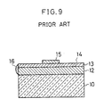
- one example of the light emitting diode produced specifically by the aforementioned MOVPE is, as shown in Fig. 9, constructed as such that an N layer 12 consisting of N-type GaN and an I layer 13 consisting of I-type GaN formed by doping zinc are formed on the sapphire substrate 10, an electrode 15 is formed on the upper surface of the I layer 13 and an electrode 16 is formed on the side of the N layer 12 so that the both layers are luminous at their joint.
- the electrode 16 Since the sapphire substrate is utilized in the light emitting diode, the electrode 16 has to be positioned on the side of the N layer 12, encountering difficulty in production.
- the sapphire substrate having the surface a ( ⁇ 11 2 0 ⁇ ) as the main surface is easy to produce, various advantages in production are obtained, for example, a blue light emitting diode can be produced easily at a low cost.
- the inventors have, by employing a mechanism of selective growth, developed the light emitting diode structure and its process of production which is easy to produce and simple to handle.
- Fig. 1 is a structural view showing an apparatus for vapor growth for producing a semiconductor and a light emitting diode according to the present invention.
- a susceptor 22 In a reaction chamber 20 surrounded by a quartz reaction tube 21, a susceptor 22 is supported by a control rod 23 for adjustment. On the main surface 22a of the susceptor 22, a sapphire substrate 24 having the main surface 24a which is subjected to the crystal growth is disposed.
- the numeral 8 generally denotes a high frequency coil for heating the sapphire substrate 24.
- a first reactant gas tube 25 and a second reactant gas tube 26 are arranged on the gas inlet side of the reaction chamber 20, a first reactant gas tube 25 and a second reactant gas tube 26 are arranged.
- the first reactant gas tube 25 is disposed concentrically within the second reactant gas tube 26, the former being connected to a first manifold 27 and the latter being connected to a second manifold 28.
- a supply system H of NH3 a supply system I of a carrier gas, a supply system J of TMG and a supply system K of TMA are connected, and to the second manifold 28, the supply system I of the carrier gas and a supply system L of DEZ are connected.
- the mixed gas When forming an N-type Al x Ga 1-x N thin film, the mixed gas may be introduced only from the first reactant gas tube 25, and when forming an I-type Al x Ga 1-x N thin film, the mixed gas may be introduced respectively from the first reactant gas tube 25 and the second reactant gas tube 26.
- DEZ which is the dopant gas is mixed with the reactant gases introduced from the first reactant gas tube 25 only at a reaction chamber 20a in the vicinity of the sapphire substrate 24. Then, DEZ is blown against the sapphire substrate and decomposed thermally, a dopant element is doped to growing Al x Ga 1-x N to yield I-type Al x Ga 1-x N.
- the openings 25a and 26a of the first and second reactant gas tubes 25, 26 and the sapphire substrate 24 are spaced at 10 to 60 mm.
- an inclined angle ⁇ of the main surface 22a of the susceptor, 22 relative to the direction X of the reactant gas flow is set at 45°. In this arrangement, a better crystal was yielded as compared with the case where the susceptor 22 is arranged normally to the gas flow.
- the GaN thin film was formed on the sapphire substrate including the surface a ( ⁇ 11 2 0 ⁇ ) as the main surface as follows.
- the single crystal sapphire substrate 24 including the surface a ( ⁇ 11 2 0 ⁇ ) as the main surface, which is cleaned with the organic cleansing and heat treatment, is disposed on the main surface 22a of the susceptor 22.
- the sapphire substrate 24 is then subjected to the vapor etching at 1100°C as feeding H2 from the first and second reactant gas tubes 25, 26 into the reaction chamber 20 at the flow rate of 0.3 l/min.
- the heat treatment was performed for 1 minute as lowering the temperature to 950°C and supplying H2 at 3 l/min. NH3 at 2 l/min. and TMA at 7 ⁇ 10 ⁇ 6 mols/min. from the first reactant gas tube 25.
- an AlN buffer layer of 0.1 ⁇ m thick was formed on the sapphire substrate 24.
- the supply of TMA was suspended after one minute and the temperature of sapphire substrate 24 was kept at 970°C, then H2 was supplied at 2.5 l/min., NH3 at 1.5 l/min. and TMG at 1.7 ⁇ 10 ⁇ 5 mols/min. for 60 minutes from the the first reactant gas tube 25 to form the GaN thin film of 7 ⁇ m thick.
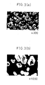
- the GaN thin film was grown as similarly as the aforementioned process. SEM images of the thin film surface are shown in Fig. 3 and its luminous characteristic by the photoluminescence is shown in Fig. 5.
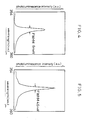
- the GaN thin film grown on the sapphire substrate of the surface a has larger and more hexagonal crystals with better crystallinity compared to those grown on the sapphire substrate of the surface c ( ⁇ 0001 ⁇ ). While, in the characteristic of the photoluminescence intensity a half-width is 4.6 meV in the case of the surface c ( ⁇ 0001 ⁇ ) and that is 6 meV in the case of the surface a ( ⁇ 11 2 0 ⁇ ). Therefore, as far as viewing from the photoluminescence intensity the crystallinity is generally same as that grown on the surface c ( ⁇ 0001 ⁇ ).
- the sapphire substrate 24 was then subjected to the vapor etching at 1100°C as feeding H2 from the first and second reactant gas tubes 25, 26 into the reaction chamber 20 at a flow rate of 0.3 l/min.
- the heat treatment was performed for 1 minute as lowering the temperature to 950°C and supplying H2 at 3 l/min., NH3 at 2 l/min. and TMA at 7 ⁇ 10 ⁇ 6 mols/min.
- a SiO2 film 32 of about 100 ⁇ film thickness was patterned. Thereafter, the photoregist was removed and the sapphire substrate 24 patterned only with the SiO2 film 32 was cleaned, remounted to the susceptor 22 and subjected to the vapor etching.
- an I layer 33 consisting of I-type GaN was grown to the film thickness of 1.0 ⁇ m.
- a conductive layer 34 consisting of polycrystalline GaN is formed. Since the conductive layer 34 is polycrystalline, it has conductivity.
- the sapphire substrate 24 was taken out from the reaction chamber 20, aluminum electrodes 35, 36 were evaporated on the I layer 33 and the conductive layer 34, and the sapphire substrate 24 was cut into a prescribed size to form the light emitting diode.
- the electrode 35 acts as the electrode for the I layer 33 and the electrode 36 for the N layer 31 through the conductive layer 34 and the very thin SiO2 film 32. Then, by bringing the I layer 33 at a positive potential with respect to the N layer 31, a junction face between the two layers becomes luminous.
- FIG. 7(a) A sectional SEM image of the I layer 33 grown on the N layer 31 is shown in Fig. 7(a) and reflective high energy electron diffraction (RHEED) pattern is shown in Fig. 8(a). Also, an SEM image of the conductive layer 34 grown on the SiO2 film 32 is shown in Fig. 7(b) and an RHEED pattern is shown in Fig. 8(b).
- N-type GaN single crystal GaN is grown and on the SiO2 film, polycrystalline GaN is grown, which has a higher conductivity as compared with the former and forms the conductive layer 34 and acts as the lead with respect to the N layer 31.
- the surface c ( ⁇ 0001 ⁇ ) was selected as the main surface of the sapphire substrate, by selecting the surface a ( ⁇ 11 2 0 ⁇ ) and employing the same process, the light emitting diode of better quality could be produced at a lower cost.
- Electrodes are formed on the I-layer and conductive layer to constitute the light emitting diode.
- a buffer layer consisting of aluminum nitride is formed, onto which a gallium nitride group semiconductor is formed.
Abstract
Description
- The present invention relates to a gallium nitride group semiconductor and a light emitting diode comprising it and the process of producing the same.
- In the past, the semiconductor and the light emitting diode formed by the vapor growth of a thin film of gallium nitride group semiconductor (AℓxGa1-xN; inclusive of x = 0) on a sapphire substrate using the process of metalorganic vapor phase epitaxy (hereinafter referred to as "MOVPE") have been studied.
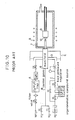
- The MOVPE forming the light emitting diode and the semiconductor is conducted by using a vopor growth apparatus as shown in Fig. 10. In the vapor growth apparatus, a
manifold 6 is connected to aquartz reaction tube 7 and a supply system A of NH₃, a supply system B of H₂ and N₂, a supply system C of trimethylgallium (hereinafter referred to as "TMG") of an organometallic compound gas, a supply system D of trimethylaluminum (hereinafter referred to as "TMA") of the organmetallic compound gas and a supply system E of diethylzinc (hereinafter referred to as "DEZ") which is a reactant gas containing a doping element (hereinafter referred to as "dopant gas") are connected to themanifold 6. Also, in thequartz reaction tube 7, a high frequency heating graphite susceptor 9 is provided, on which asapphire substrate 10 is disposed, which is heated by a high frequency coil 8. Each reactant gas and carrier gas from each supply system are mixed in themanifold 6, and the mixed gas is led to thequartz reaction tube 7 and blown against thesapphire substrate 10 to grow an AℓxGa1-xN thin film thereon. - Then, by changing the mixing ratio of each organometallic compound gas, the composition ratio can be changed and the insulated thin film of I-type (Intrinsic) AℓxGa1-xN can be formed by doping zinc.
- Also, one example of the light emitting diode produced specifically by the aforementioned MOVPE is, as shown in Fig. 9, constructed as such that an N layer 12 consisting of N-type GaN and an
I layer 13 consisting of I-type GaN formed by doping zinc are formed on thesapphire substrate 10, anelectrode 15 is formed on the upper surface of theI layer 13 and anelectrode 16 is formed on the side of the N layer 12 so that the both layers are luminous at their joint. - Since the sapphire substrate is utilized in the light emitting diode, the
electrode 16 has to be positioned on the side of the N layer 12, encountering difficulty in production. - Meanwhile, when forming the
electrode 16 of the N layer 12 on the same surface as theelectrode 15 of the Ilayer 13, it has been attempted to form the electrode on the N layer exposed by removing an insulated film, after selectively forming the I layer by masking with the insulated film evaporated in a prescribed pattern. - However, since selective growth of the I layer with the insulated film mask is somewhat difficult and the I layer is formed also on the insulated film, making removal of the insulated film alone is difficult.
- In the past, when the vapor growth of the gallium nitride group semiconductor takes place on the sapphire substrate, a surface c ({0001}) has been considered appropriate as the main surface which is involved in the crystal growth.
- The inventors have discovered that by forming an AℓN buffer layer on a surface a ({11
2 0}) of a sapphire substrate and growing a thin film of AℓxGa1-xN (inclusive of x = 0) thereon, crystallinity of AℓxGa1-xN can be improved. - According to the present invention, since the sapphire substrate having the surface a ({11
2 0}) as the main surface is easy to produce, various advantages in production are obtained, for example, a blue light emitting diode can be produced easily at a low cost. - Also, the inventors have, by employing a mechanism of selective growth, developed the light emitting diode structure and its process of production which is easy to produce and simple to handle.
- That is, by pattern forming an SiO₂ thin film on the N layer consisting of AℓxGa1-xN (inclusive of x = 0) and growing I-type AℓxGa1-xN (inclusive of x = 0) thereon, portions on the N layer become the I layer as the active layer, and the other portions growing on the SiO₂ thin film become the conductive layer showing conductivity because they are non-single crystal. Thus, there is such an advantage as forming the I layer and conductive layer at the same time, and by forming the electrodes on the both layers the light emitting diode can be constructed to take out a lead wire from the same plane.
- It is, therefore, a primary object of the present invention to provide a blue light emitting diode which is easy to produce and high in quality and the process of producing the same.
- It is another object of the present invention to provide a gallium nitride group semiconductor growing on the sapphire substrate and having a good quality and the process of producing the same.
- It is a further object of the present invention to provide a light emitting diode which is easy to produce and simple to handle and having electrodes formed on the same plane.
-
- Fig. 1 is a structural view showing an apparatus for vapor growth for embodying the present invention.
- Fig. 2(a) and Fig. 2(b) are SEM images showing a surface morphology of a GaN thin film grown on a surface a ({11
2 0}) of a sapphire substrate. - Fig. 3(a) and Fig. 3(b) are SEM images showing a surface morphology of a GaN thin film grown on a surface c ({0001}) of a sapphire substrate.
- Fig. 4 is a measured curve showing a photoluminescence intensity characteristic of a GaN thin film grown on a surface a ({11
2 0}) of a sapphire substrate. - Fig. 5 is a measured curve showing a photoluminescence intensity characteristic of a GaN thin film grown on a surface c ({0001}) of a sapphire substrate.
- Fig. 6 is a sectional view showing the structure of a light emitting diode.
- Fig. 7(a) is an SEM image showing a sectional construction of a GaN layer grown on an N layer.
- Fig. 7(b) is an SEM image showing a sectional construc tion of a GaN layer grown on a SiO₂ thin film.
- Fig. 8(a) is an RHEED pattern of a GaN layer grown on an N layer.
- Fig. 8(b) is an RHEED pattern of a GaN layer grown on a SiO₂ film.
- Fig. 9 is a sectional view showing the structure of a conventional light emitting diode.
- Fig. 10 is a structural view showing the structure of a conventional apparatus for vapor growth.
- The present invention will be described in the following referring to the specific embodiment. Fig. 1 is a structural view showing an apparatus for vapor growth for producing a semiconductor and a light emitting diode according to the present invention.
- In a reaction chamber 20 surrounded by a
quartz reaction tube 21, asusceptor 22 is supported by acontrol rod 23 for adjustment. On the main surface 22a of thesusceptor 22, asapphire substrate 24 having the main surface 24a which is subjected to the crystal growth is disposed. The numeral 8 generally denotes a high frequency coil for heating thesapphire substrate 24. - Meanwhile, on the gas inlet side of the reaction chamber 20, a first
reactant gas tube 25 and a secondreactant gas tube 26 are arranged. The firstreactant gas tube 25 is disposed concentrically within the secondreactant gas tube 26, the former being connected to afirst manifold 27 and the latter being connected to asecond manifold 28. To thefirst manifold 27, a supply system H of NH₃, a supply system I of a carrier gas, a supply system J of TMG and a supply system K of TMA are connected, and to thesecond manifold 28, the supply system I of the carrier gas and a supply system L of DEZ are connected. - Since the apparatus is constructed as such, from the opening 25a of the first
reactant gas tube 25, mixed gas of NH₃, TMG, TMA and H₂ flows out into the reaction chamber 20, and from the opening 26a of the secondreactant gas tube 26, a mixed gas of DEZ and H₂ flows out into the reaction chamber 20. - When forming an N-type AℓxGa1-xN thin film, the mixed gas may be introduced only from the first
reactant gas tube 25, and when forming an I-type AℓxGa1-xN thin film, the mixed gas may be introduced respectively from the firstreactant gas tube 25 and the secondreactant gas tube 26. When forming the I-type AℓxGa1-xN thin film, DEZ which is the dopant gas is mixed with the reactant gases introduced from the firstreactant gas tube 25 only at areaction chamber 20a in the vicinity of thesapphire substrate 24. Then, DEZ is blown against the sapphire substrate and decomposed thermally, a dopant element is doped to growing AℓxGa1-xN to yield I-type AℓxGa1-xN. In this case, since the reactant gas and dopant gas are completely separated by the first and secondreactant gas tubes reaction chamber 20a near thesapphire substrate 24, reaction between DEZ and TMG or TMA within the feed tube of the gas occurred in the prior art apparatus is restrained, so that the doping is effected satisfactorily. - It is preferable that the
openings 25a and 26a of the first and secondreactant gas tubes sapphire substrate 24 are spaced at 10 to 60 mm. Also, an inclined angle ϑ of the main surface 22a of the susceptor, 22 relative to the direction X of the reactant gas flow is set at 45°. In this arrangement, a better crystal was yielded as compared with the case where thesusceptor 22 is arranged normally to the gas flow. - Next, utilizing the apparatus for vapor growth, the GaN thin film was formed on the sapphire substrate including the surface a ({11
2 0}) as the main surface as follows. - First, the single
crystal sapphire substrate 24 including the surface a ({112 0}) as the main surface, which is cleaned with the organic cleansing and heat treatment, is disposed on the main surface 22a of thesusceptor 22. Thesapphire substrate 24 is then subjected to the vapor etching at 1100°C as feeding H₂ from the first and secondreactant gas tubes reactant gas tube 25. By the heat treatment, an AℓN buffer layer of 0.1 µm thick was formed on thesapphire substrate 24. The supply of TMA was suspended after one minute and the temperature ofsapphire substrate 24 was kept at 970°C, then H₂ was supplied at 2.5 ℓ/min., NH₃ at 1.5 ℓ/min. and TMG at 1.7 × 10⁻⁵ mols/min. for 60 minutes from the the firstreactant gas tube 25 to form the GaN thin film of 7 µm thick. - SEM images of the GaN thin film surface thus formed are shown in Fig. 2 and its luminous characteristic by the photoluminescence is shown in Fig. 4.
- Meanwhile, also on the sapphire substrate including the surface c ({0001}) as the main surface, the GaN thin film was grown as similarly as the aforementioned process. SEM images of the thin film surface are shown in Fig. 3 and its luminous characteristic by the photoluminescence is shown in Fig. 5.
- As it is apparent from SEM image, the GaN thin film grown on the sapphire substrate of the surface a ({11
2 0}) has larger and more hexagonal crystals with better crystallinity compared to those grown on the sapphire substrate of the surface c ({0001}). While, in the characteristic of the photoluminescence intensity a half-width is 4.6 meV in the case of the surface c ({0001}) and that is 6 meV in the case of the surface a ({112 0}). Therefore, as far as viewing from the photoluminescence intensity the crystallinity is generally same as that grown on the surface c ({0001}). - A process of producing a light emitting diode by the crystal growth of GaN on the sapphire substrate will be now described referring to Fig. 1 and Fig. 6.
- The single
crystal sapphire substrate 24 including the surface c ({0001}) as the main surface, which is cleaned by the organic cleansing and heat treatment, is first disposed on the main surface 22a of thesusceptor 22. Thesapphire substrate 24 was then subjected to the vapor etching at 1100°C as feeding H₂ from the first and secondreactant gas tubes reactant gas tube 25, thereby a 0.1 µm thickAℓN buffer layer 30 was formed. As suspending the supply of TMA after 1 minute and keeping the temperature of thesapphire substrate 24 at 970°C, H₂ was supplied at 2.5 ℓ/min., NH₃ at 1.5 ℓ/min. and TMG at 1.7 × 10⁻⁵ mols/min. from the firstreactant gas tube 25 for 60 minutes to form an N layer 31 consisting of the N-type GaN thin film of about 7 µm thick. Next, thesapphire substrate 24 was taken out from the reaction chamber 20, and the main surface of the N layer 31 coated with a photoregist was etched after being exposed by using a mask with prescribed pattern to form the photoregist with prescribed pattern thereon. Using the photoregist as the mask, a SiO₂ film 32 of about 100 Å film thickness was patterned. Thereafter, the photoregist was removed and thesapphire substrate 24 patterned only with the SiO₂ film 32 was cleaned, remounted to thesusceptor 22 and subjected to the vapor etching. - Then, as keeping the temperature of the
sapphire substrate 24 at 970°C and feeding H₂ at 2.5 ℓ/min., NH₃ at 1.5 ℓ/min. and TMG at 1.7 × 10⁻⁵ mols/min. from the firstreactant gas tube 25, and DEZ at 5 × 10⁻⁶ mols/min. from the secondreactant gas tube 26 for 5 minutes, anI layer 33 consisting of I-type GaN was grown to the film thickness of 1.0 µm. At this time, on the window portion where the N layer 31 of GaN is exposed, single crystal I-type GaN is grown to yield theI layer 33, but on the SiO₂ film 32, aconductive layer 34 consisting of polycrystalline GaN is formed. Since theconductive layer 34 is polycrystalline, it has conductivity. - Then, the
sapphire substrate 24 was taken out from the reaction chamber 20,aluminum electrodes I layer 33 and theconductive layer 34, and thesapphire substrate 24 was cut into a prescribed size to form the light emitting diode. In this case, theelectrode 35 acts as the electrode for theI layer 33 and theelectrode 36 for the N layer 31 through theconductive layer 34 and the very thin SiO₂ film 32. Then, by bringing theI layer 33 at a positive potential with respect to the N layer 31, a junction face between the two layers becomes luminous. - A sectional SEM image of the
I layer 33 grown on the N layer 31 is shown in Fig. 7(a) and reflective high energy electron diffraction (RHEED) pattern is shown in Fig. 8(a). Also, an SEM image of theconductive layer 34 grown on the SiO₂ film 32 is shown in Fig. 7(b) and an RHEED pattern is shown in Fig. 8(b). As it will be apparent from these photographs, on N-type GaN, single crystal GaN is grown and on the SiO₂ film, polycrystalline GaN is grown, which has a higher conductivity as compared with the former and forms theconductive layer 34 and acts as the lead with respect to the N layer 31. - In forming the AℓxGa1-xN group light emitting diode, TMA may be introduced from the first
reactant gas tube 25 at a prescribed rate when forming the N layer 31 and Ilayer 33. For example, by maintaining the temperature of thesapphire substrate 24 at 1105°C and supplying H₂ at 3 ℓ/min., NH₃ at 2 ℓ/min., TMA at 7.2 × 10⁻⁶ mols/min. and TMG at 1.7 × 10⁻⁵ mols/min. from the firstreactant gas tube 25 and DEZ at 5 × 10⁻⁶ mols/min. from the secondreactant gas tube 26, the I-type AℓxGa1-xN (x = 0.3) group semiconductor thin film can be obtained. - In the light emitting diode mentioned above, though the surface c ({0001}) was selected as the main surface of the sapphire substrate, by selecting the surface a ({11
2 0}) and employing the same process, the light emitting diode of better quality could be produced at a lower cost. - A thin film of SiO₂ is patterned on an N layer consisting of N-type AℓxGa1-xN (inclusive of x = 0). Next, I-type AℓxGa1-xN (inclusive of x = 0) is selectively grown and the portion on the N layer grows into an I-layer consisting an active layer of a light emitting diode, and that on the SiO₂ thin film grows into a conductive layer. Electrodes are formed on the I-layer and conductive layer to constitute the light emitting diode. Also, on the surface a ({11
2 0}) of a sapphire substrate, a buffer layer consisting of aluminum nitride is formed, onto which a gallium nitride group semiconductor is formed.
Claims (11)
- (1) A gallium nitride group semiconductor light emitting diode having,
an N layer consisting of an N-type gallium nitride group semiconductor (AℓxGa1-xN; inclusive of x = 0),
an SiO₂ thin film patterned on the main surface of said N layer,
an I layer selectively developed by doping impurities on said N layer onto which said SiO₂ thin film is patterned, and consisting of an I-type gallium nitride group semiconductor (AℓxGa1-xN; inclusive of x = 0) joined to said N layer,
a non-single crystal conductive layer formed on said SiO₂ thin film with the growth of said I layer, and
electrode layers joined to the surface of said I layer and said conductive layer. - (2) A gallium nitride group semiconductor light emitting diode having,
a sapphire substrate,
a buffer layer consisting of aluminum nitride (AℓN) formed on the main surface of said sapphire substrate,
an N layer consisting of an N-type gallium nitride group semiconductor (AℓxGa1-xN; inclusive of x = 0) formed on said buffer layer,
an SiO₂ thin film patterned on the main surface of said N layer,
an I layer selectively grown by doping impurities on said N layer onto which said SiO₂ thin film is patterned, and consisting of an I-type gallium nitride group semiconductor (AℓxGa1-xN; inclusive of x = 0) joined to said N layer,
a non-single crystal conductive layer formed on said SiO₂ thin film with the growth of said I layer, and
electrode layers joined to the surface of said I layer and said conductive layer. - (3) A gallium nitride group semiconductor light emitting diode as claimed in claim 2, wherein the main surface of said sapphire substrate is a surface a ({11
2 0}). - (4) A gallium nitride group semiconductor light emitting diode as claimed in claim 2,
wherein the main surface of said sapphire substrate is a surface c ({0001}). - (5) A process of producing a gallium nitride group semiconductor light emitting diode, whereby a SiO₂ thin film patterned to open the portion corresponding to an active layer of the light emitting diode is formed on the main surface of an N layer substrate consisting of an N-type gallium nitride group semiconductor (AℓxGa1-xN; of inclusive x = 0),
then, by growing the gallium nitride group semiconductor (AℓxGA1-xN; inclusive of x = 0) doped with impurities, on the main surface of said N layer substrate onto which said SiO₂ thin film is patterned, an I layer consisting of an I-type single crystal gallium nitride group semiconductor (AℓxGa1-xN; inclusive of x = 0) is formed on the portion joined to said N layer substrate,
a conductive layer consisting of a non-single crystal gallium nitride group semiconductor (AℓxGa1-xN; inclusive of x = 0) is formed on the portion joined to said SiO₂ thin film, and
electrode layers joined to the surface of said I layer and said conductive layer are formed. - (6) A process of producing a gallium nitride group semiconductor light emitting diode, whereby a buffer layer consisting of aluminum nitride (AℓN) is formed on the main surface of a sapphire substrate,
an N layer consisting of an N-type gallium nitride group semiconductor (AℓxGa1-xN; inclusive of x = 0) is formed on said buffer layer,
an SiO₂ thin film patterned to open the portion corresponding to an active layer of the light emitting diode is formed on the main surface of said N layer,
then, by growing the gallium nitride group semiconductor (AℓxGa1-xN; inclusive of x = 0) doped with impurities, on the main surface of said N layer substrate onto which said SiO₂ thin film is patterned,
an I layer consisting of an I-type single crystal gallium nitride group semiconductor (AℓxGa1-xN; inclusive of x = 0) is formed at the portion joined to said N layer substrate,
a conductive layer consisting of a non-single crystal gallium nitride group semiconductor (AℓxGa1-xN; inclusive x = 0) is formed at the portion joined to said SiO₂ thin film, and
electrode layers joined to the surface of said I layer and said conductive layer are formed. - (7) The process of producing a gallium nitride group semiconductor light emitting diode as claimed in claim 6, wherein the main surface of said sapphire substrate is a surface a ({11
2 0}). - (8) The process of producing a gallium nitride group semiconductor light emitting diode as claimed in claim 6, wherein the main surface of said sapphire substrate is a surface c ({0001}).
- (9) A gallium nitride group semiconductor light emitting diode having,
a sapphire substrate including a surface a ({112 0}) as the main surface, and
a buffer layer consisting of aluminum nitride (AℓN) formed on the main surface of said sapphire substrate. - (10) A gallium nitride group semiconductor having,
a sapphire substrate including a surface a ({112 0}) as the main surface, and
a buffer layer consisting of aluminum nitride (AℓN) formed on the main surface of said sapphire substrate. - (11) A process of vapor growth of a gallium nitride group semiconductor thin film using an organometallic compound gas, characterized in that a buffer layer consisting of aluminum nitride is grown on a surface a ({11
2 0}) of a sapphire substrate, and the vapor growth of the gallium nitride group semiconductor (AℓxGa1-xN; inclusive of x = 0) thin film is performed on the buffer layer.
Priority Applications (1)
| Application Number | Priority Date | Filing Date | Title |
|---|---|---|---|
| EP91113265A EP0460710B1 (en) | 1987-01-31 | 1988-01-28 | Gallium nitride group compound semiconductor and luminous element comprising it and the process of producing the same |
Applications Claiming Priority (4)
| Application Number | Priority Date | Filing Date | Title |
|---|---|---|---|
| JP21126/87 | 1987-01-31 | ||
| JP21124/87 | 1987-01-31 | ||
| JP2112487A JPH079999B2 (en) | 1987-01-31 | 1987-01-31 | Gallium nitride compound semiconductor light emitting device |
| JP62021126A JPS63188938A (en) | 1987-01-31 | 1987-01-31 | Method for vapor growth of gallium nitride compound semiconductor |
Related Child Applications (2)
| Application Number | Title | Priority Date | Filing Date |
|---|---|---|---|
| EP91113265.2 Division-Into | 1988-01-28 | ||
| EP91113265A Division EP0460710B1 (en) | 1987-01-31 | 1988-01-28 | Gallium nitride group compound semiconductor and luminous element comprising it and the process of producing the same |
Publications (3)
| Publication Number | Publication Date |
|---|---|
| EP0277597A2 true EP0277597A2 (en) | 1988-08-10 |
| EP0277597A3 EP0277597A3 (en) | 1989-09-20 |
| EP0277597B1 EP0277597B1 (en) | 1994-07-13 |
Family
ID=26358145
Family Applications (2)
| Application Number | Title | Priority Date | Filing Date |
|---|---|---|---|
| EP88101267A Expired - Lifetime EP0277597B1 (en) | 1987-01-31 | 1988-01-28 | Gallium nitride group semiconductor light emitting diode and the process of producing the same |
| EP91113265A Expired - Lifetime EP0460710B1 (en) | 1987-01-31 | 1988-01-28 | Gallium nitride group compound semiconductor and luminous element comprising it and the process of producing the same |
Family Applications After (1)
| Application Number | Title | Priority Date | Filing Date |
|---|---|---|---|
| EP91113265A Expired - Lifetime EP0460710B1 (en) | 1987-01-31 | 1988-01-28 | Gallium nitride group compound semiconductor and luminous element comprising it and the process of producing the same |
Country Status (2)
| Country | Link |
|---|---|
| EP (2) | EP0277597B1 (en) |
| DE (2) | DE3850582T2 (en) |
Cited By (14)
| Publication number | Priority date | Publication date | Assignee | Title |
|---|---|---|---|---|
| EP0383215A2 (en) * | 1989-02-13 | 1990-08-22 | Nippon Telegraph And Telephone Corporation | Epitaxial-growth structure for a semiconductor light-emitting device, and semiconductor light-emitting device using the same |
| DE4006449A1 (en) * | 1989-03-01 | 1990-09-13 | Toyoda Gosei Kk | SUBSTRATE FOR GROWING A GALLIUM NITRIDE CONNECTION SEMICONDUCTOR DEVICE AND LIGHT EMITTER DIODE |
| EP0444630A1 (en) * | 1990-02-28 | 1991-09-04 | Toyoda Gosei Co., Ltd. | Light-emitting semiconductor device using gallium nitride group compound |
| EP0459469A1 (en) * | 1990-05-30 | 1991-12-04 | Toyoda Gosei Co., Ltd. | Dry etching method for semiconductor |
| EP0483688A2 (en) * | 1990-10-27 | 1992-05-06 | Toyoda Gosei Co., Ltd. | Light emitting semiconductor device using gallium nitride group compound |
| US5278433A (en) * | 1990-02-28 | 1994-01-11 | Toyoda Gosei Co., Ltd. | Light-emitting semiconductor device using gallium nitride group compound with double layer structures for the n-layer and/or the i-layer |
| GB2273391A (en) * | 1992-11-20 | 1994-06-15 | Mitsubishi Electric Corp | Apparatus for growing compound semiconductor layers |
| US5408120A (en) * | 1992-07-23 | 1995-04-18 | Toyoda Gosei Co., Ltd. | Light-emitting device of gallium nitride compound semiconductor |
| EP0852416A1 (en) * | 1995-09-18 | 1998-07-08 | Hitachi, Ltd. | Semiconductor material, method of producing the semiconductor material, and semiconductor device |
| US6362017B1 (en) | 1990-02-28 | 2002-03-26 | Toyoda Gosei Co., Ltd. | Light-emitting semiconductor device using gallium nitride group compound |
| US6830992B1 (en) | 1990-02-28 | 2004-12-14 | Toyoda Gosei Co., Ltd. | Method for manufacturing a gallium nitride group compound semiconductor |
| CN100428410C (en) * | 2002-01-09 | 2008-10-22 | 南京大学 | Homogeneity improving method and device for hydride gaseous epitaxially groven GaN material |
| US7663157B2 (en) | 1991-03-18 | 2010-02-16 | The Trustees Of Boston University | Semiconductor device having group III nitride buffer layer and growth layers |
| DE19640594B4 (en) * | 1996-10-01 | 2016-08-04 | Osram Gmbh | module |
Families Citing this family (3)
| Publication number | Priority date | Publication date | Assignee | Title |
|---|---|---|---|---|
| JP3352712B2 (en) * | 1991-12-18 | 2002-12-03 | 浩 天野 | Gallium nitride based semiconductor device and method of manufacturing the same |
| US5739554A (en) * | 1995-05-08 | 1998-04-14 | Cree Research, Inc. | Double heterojunction light emitting diode with gallium nitride active layer |
| JPH08316582A (en) * | 1995-05-19 | 1996-11-29 | Nec Corp | Semiconductor laser |
Citations (9)
| Publication number | Priority date | Publication date | Assignee | Title |
|---|---|---|---|---|
| US3683240A (en) * | 1971-07-22 | 1972-08-08 | Rca Corp | ELECTROLUMINESCENT SEMICONDUCTOR DEVICE OF GaN |
| US4152182A (en) * | 1978-05-15 | 1979-05-01 | International Business Machines Corporation | Process for producing electronic grade aluminum nitride films utilizing the reduction of aluminum oxide |
| DE3046018A1 (en) * | 1979-12-05 | 1981-09-03 | Matsushita Electric Industrial Co., Ltd., 1006 Kadoma, Osaka | ELECTROLUMINISCENCE SEMICONDUCTOR COMPONENT WITH GALLIUM NITRIDE AND METHOD FOR THE PRODUCTION THEREOF |
| JPS56150880A (en) * | 1980-04-23 | 1981-11-21 | Matsushita Electric Ind Co Ltd | Gallium nitride light emitting element chip and manufacture thereof |
| JPS57102081A (en) * | 1980-12-17 | 1982-06-24 | Matsushita Electric Ind Co Ltd | Manufacture of luminous element |
| US4404265A (en) * | 1969-10-01 | 1983-09-13 | Rockwell International Corporation | Epitaxial composite and method of making |
| GB2123607A (en) * | 1982-02-02 | 1984-02-01 | Bagratishvili Givi D | Semiconductor light emitting device on gallium nitride base and method for manufacture thereof |
| JPS59228776A (en) * | 1983-06-10 | 1984-12-22 | Nippon Telegr & Teleph Corp <Ntt> | Semiconductor hetero-junction element |
| JPS60175468A (en) * | 1984-02-21 | 1985-09-09 | Matsushita Electric Ind Co Ltd | Manufacture of gallium nitride semiconductor device |
-
1988
- 1988-01-28 EP EP88101267A patent/EP0277597B1/en not_active Expired - Lifetime
- 1988-01-28 DE DE19883850582 patent/DE3850582T2/en not_active Expired - Lifetime
- 1988-01-28 DE DE19883852402 patent/DE3852402T2/en not_active Expired - Lifetime
- 1988-01-28 EP EP91113265A patent/EP0460710B1/en not_active Expired - Lifetime
Patent Citations (9)
| Publication number | Priority date | Publication date | Assignee | Title |
|---|---|---|---|---|
| US4404265A (en) * | 1969-10-01 | 1983-09-13 | Rockwell International Corporation | Epitaxial composite and method of making |
| US3683240A (en) * | 1971-07-22 | 1972-08-08 | Rca Corp | ELECTROLUMINESCENT SEMICONDUCTOR DEVICE OF GaN |
| US4152182A (en) * | 1978-05-15 | 1979-05-01 | International Business Machines Corporation | Process for producing electronic grade aluminum nitride films utilizing the reduction of aluminum oxide |
| DE3046018A1 (en) * | 1979-12-05 | 1981-09-03 | Matsushita Electric Industrial Co., Ltd., 1006 Kadoma, Osaka | ELECTROLUMINISCENCE SEMICONDUCTOR COMPONENT WITH GALLIUM NITRIDE AND METHOD FOR THE PRODUCTION THEREOF |
| JPS56150880A (en) * | 1980-04-23 | 1981-11-21 | Matsushita Electric Ind Co Ltd | Gallium nitride light emitting element chip and manufacture thereof |
| JPS57102081A (en) * | 1980-12-17 | 1982-06-24 | Matsushita Electric Ind Co Ltd | Manufacture of luminous element |
| GB2123607A (en) * | 1982-02-02 | 1984-02-01 | Bagratishvili Givi D | Semiconductor light emitting device on gallium nitride base and method for manufacture thereof |
| JPS59228776A (en) * | 1983-06-10 | 1984-12-22 | Nippon Telegr & Teleph Corp <Ntt> | Semiconductor hetero-junction element |
| JPS60175468A (en) * | 1984-02-21 | 1985-09-09 | Matsushita Electric Ind Co Ltd | Manufacture of gallium nitride semiconductor device |
Non-Patent Citations (12)
| Title |
|---|
| Applied Physics Letters, Vol. 48, No, 5, 1986, 3rd February, pages 353-355, New York, NY, US; H. AMANO et al.: "Metalorganic vapor phase epitaxial growth of a high quality GaN film using an AIN buffer layer". * |
| APPLIES PHYSICS LETTERS, vol. 48, no. 5, 3 Febaruary 1986, pages 353-355, New York, US; H. AMANO et al.: "Metalorganic vapor phase epitaxial growth of a high quality GaN film using an AIN buffer layer" * |
| Crystal Research and Technology, Vol. 15, No. 10, 1980, pages 1143-1149, East-Berlin, DDR; G. FITZL et al.: "Epitaxial Growth of GaN on (1012) oriented Sapphire in GaCI/NH 3/He and GaCI/NH3/H2 Systems". * |
| Journal of Applied Physics, Vol. 56, No, 8, October 1984, pages 2367-2368, Woodbury, New York, USA; T. KAWABATA et al.: "GaN blue light emitting diodes prepared by metalorganic chemical vapor deposition". * |
| Journal of Applied Physics, Vol. 56, No. 8, October 1984, pages 2367-2368, Woodbury, New York, US; T. KAWABATA et al.: "GaN blue light emitting diodes prepared by metalorganic chemical vapor deposition". * |
| Journal of the Electrochemical Society, Vol. 125, No. 12, December 1978, pages 2076-2078; A SHINTANI et al.: "X-Ray Diffraction Topography and Crystal Characterization of GaN Epitaxial Layers for Light-Emitting Diodes". * |
| Journal of the Electrochemical, Vol. 125, No. 12, December 1978, pages 2076-2078, US; A. SHINTANI et al.: "X-Ray Diffraction Topography and Crystal Characterization of GaN Epitaxial Layers for Light-Emitting Diodes". * |
| PATENT ABSTRACTS OF JAPAN, vol. 10, no. 11 (E-374)(2068), 17 January 1985; & JP-A-60 175 468 (MATSUSHITA DENKI SANGYO) 09-09-1985 * |
| PATENT ABSTRACTS OF JAPAN, Vol. 10, No. 11 (E-374)(2068), 17th January 1986; & JP-A-60 175 468 (MATSUSHITA DENKI SANGYO) 09-09-1985. * |
| PATENT ABSTRACTS OF JAPAN, Vol. 6, No. 189 (E-133)(1067), 28th September 1982; & JP-A-57 102 081 (MATSUSHITA DENKI SANGYO) 24-06-1982 * |
| PATENT ABSTRACTS OF JAPAN, Vol. 6, No. 32 (E-96)(910), 26th February 1982; & JP-A-56 150 880 (MATSUSHITA DENKI SANGYO) 21-11-1981 * |
| PATENT ABSTRACTS OF JAPAN, Vol. 9, No. 102 (E-312)(1825), 4th May 1985; & JP-A-59 228 776 (NIPPON DENSHIN DENWA KOSHA) 22-12-1984 * |
Cited By (27)
| Publication number | Priority date | Publication date | Assignee | Title |
|---|---|---|---|---|
| EP0383215A2 (en) * | 1989-02-13 | 1990-08-22 | Nippon Telegraph And Telephone Corporation | Epitaxial-growth structure for a semiconductor light-emitting device, and semiconductor light-emitting device using the same |
| EP0383215A3 (en) * | 1989-02-13 | 1991-01-09 | Nippon Telegraph And Telephone Corporation | Epitaxial-growth structure for a semiconductor light-emitting device, and semiconductor light-emitting device using the same |
| DE4006449A1 (en) * | 1989-03-01 | 1990-09-13 | Toyoda Gosei Kk | SUBSTRATE FOR GROWING A GALLIUM NITRIDE CONNECTION SEMICONDUCTOR DEVICE AND LIGHT EMITTER DIODE |
| US6472689B1 (en) | 1990-02-28 | 2002-10-29 | Toyoda Gosei Co., Ltd. | Light emitting device |
| US6362017B1 (en) | 1990-02-28 | 2002-03-26 | Toyoda Gosei Co., Ltd. | Light-emitting semiconductor device using gallium nitride group compound |
| US6984536B2 (en) | 1990-02-28 | 2006-01-10 | Toyoda Gosei Co., Ltd. | Method for manufacturing a gallium nitride group compound semiconductor |
| US6830992B1 (en) | 1990-02-28 | 2004-12-14 | Toyoda Gosei Co., Ltd. | Method for manufacturing a gallium nitride group compound semiconductor |
| US5278433A (en) * | 1990-02-28 | 1994-01-11 | Toyoda Gosei Co., Ltd. | Light-emitting semiconductor device using gallium nitride group compound with double layer structures for the n-layer and/or the i-layer |
| US6607595B1 (en) | 1990-02-28 | 2003-08-19 | Toyoda Gosei Co., Ltd. | Method for producing a light-emitting semiconductor device |
| US6593599B1 (en) | 1990-02-28 | 2003-07-15 | Japan Science And Technology Corporation | Light-emitting semiconductor device using gallium nitride group compound |
| US5733796A (en) * | 1990-02-28 | 1998-03-31 | Toyoda Gosei Co., Ltd. | Light-emitting semiconductor device using gallium nitride group compound |
| US6472690B1 (en) | 1990-02-28 | 2002-10-29 | Toyoda Gosei Co., Ltd. | Gallium nitride group compound semiconductor |
| EP0444630A1 (en) * | 1990-02-28 | 1991-09-04 | Toyoda Gosei Co., Ltd. | Light-emitting semiconductor device using gallium nitride group compound |
| US6249012B1 (en) | 1990-02-28 | 2001-06-19 | Toyoda Gosei Co., Ltd. | Light emitting semiconductor device using gallium nitride group compound |
| US5205905A (en) * | 1990-05-30 | 1993-04-27 | Toyoda Gosei Co., Ltd. | Dry etching method for semiconductor |
| EP0459469A1 (en) * | 1990-05-30 | 1991-12-04 | Toyoda Gosei Co., Ltd. | Dry etching method for semiconductor |
| US5281830A (en) * | 1990-10-27 | 1994-01-25 | Toyoda Gosei Co., Ltd. | Light-emitting semiconductor device using gallium nitride group compound |
| EP0483688A3 (en) * | 1990-10-27 | 1992-07-15 | Toyoda Gosei Co., Ltd. | Light emitting semiconductor device using gallium nitride group compound |
| EP0483688A2 (en) * | 1990-10-27 | 1992-05-06 | Toyoda Gosei Co., Ltd. | Light emitting semiconductor device using gallium nitride group compound |
| US7663157B2 (en) | 1991-03-18 | 2010-02-16 | The Trustees Of Boston University | Semiconductor device having group III nitride buffer layer and growth layers |
| US5408120A (en) * | 1992-07-23 | 1995-04-18 | Toyoda Gosei Co., Ltd. | Light-emitting device of gallium nitride compound semiconductor |
| GB2273391A (en) * | 1992-11-20 | 1994-06-15 | Mitsubishi Electric Corp | Apparatus for growing compound semiconductor layers |
| US6459712B2 (en) | 1995-09-18 | 2002-10-01 | Hitachi, Ltd. | Semiconductor devices |
| EP0852416A4 (en) * | 1995-09-18 | 1999-04-07 | Hitachi Ltd | Semiconductor material, method of producing the semiconductor material, and semiconductor device |
| EP0852416A1 (en) * | 1995-09-18 | 1998-07-08 | Hitachi, Ltd. | Semiconductor material, method of producing the semiconductor material, and semiconductor device |
| DE19640594B4 (en) * | 1996-10-01 | 2016-08-04 | Osram Gmbh | module |
| CN100428410C (en) * | 2002-01-09 | 2008-10-22 | 南京大学 | Homogeneity improving method and device for hydride gaseous epitaxially groven GaN material |
Also Published As
| Publication number | Publication date |
|---|---|
| EP0277597B1 (en) | 1994-07-13 |
| EP0460710A2 (en) | 1991-12-11 |
| DE3852402T2 (en) | 1995-05-04 |
| EP0460710A3 (en) | 1991-12-18 |
| DE3852402D1 (en) | 1995-01-19 |
| EP0277597A3 (en) | 1989-09-20 |
| EP0460710B1 (en) | 1994-12-07 |
| DE3850582D1 (en) | 1994-08-18 |
| DE3850582T2 (en) | 1994-11-10 |
Similar Documents
| Publication | Publication Date | Title |
|---|---|---|
| US5218216A (en) | Gallium nitride group semiconductor and light emitting diode comprising it and the process of producing the same | |
| US5122845A (en) | Substrate for growing gallium nitride compound-semiconductor device and light emitting diode | |
| EP0460710B1 (en) | Gallium nitride group compound semiconductor and luminous element comprising it and the process of producing the same | |
| US4855249A (en) | Process for growing III-V compound semiconductors on sapphire using a buffer layer | |
| KR940001249B1 (en) | SILICON-GaAs EPITAXIAL COMPOSITIONS AND PROCESS FOR MAKING THE SAME | |
| JPH0573252B2 (en) | ||
| JP2000044400A (en) | Gallium nitride single crystal substrate and its production | |
| JP2000091234A (en) | Manufacture of iii-v nitride compound semiconductor | |
| JPH08325094A (en) | Preparation of iii-v group compound semiconductor | |
| JP2002249400A (en) | Method for manufacturing compound semiconductor single crystal and utilization thereof | |
| JPH0331678B2 (en) | ||
| JPH079999B2 (en) | Gallium nitride compound semiconductor light emitting device | |
| CN107794567A (en) | Method for manufacturing III nitride semiconductor | |
| TW201312788A (en) | Vapor phase epitaxy method and light emitting element substrate manufacturing method | |
| JPH0529220A (en) | Gallium nitride thin film growing method | |
| JP2704223B2 (en) | Semiconductor element | |
| JP2631286B2 (en) | Gas phase growth method of gallium nitride based compound semiconductor | |
| JP3348656B2 (en) | Gallium nitride based compound semiconductor light emitting device | |
| JPH08264464A (en) | Vapor-phase epitaxy | |
| JPH0754802B2 (en) | Vapor growth method of GaAs thin film | |
| JPH07283436A (en) | Iii-v compound semiconductor and light-emitting element | |
| JPH08335555A (en) | Fabrication of epitaxial wafer | |
| JP3534252B2 (en) | Vapor phase growth method | |
| JP2566800B2 (en) | Light emitting device manufacturing method | |
| JPH11268996A (en) | Method for growing compound semiconductor mixed crystal |
Legal Events
| Date | Code | Title | Description |
|---|---|---|---|
| PUAI | Public reference made under article 153(3) epc to a published international application that has entered the european phase |
Free format text: ORIGINAL CODE: 0009012 |
|
| 17P | Request for examination filed |
Effective date: 19880128 |
|
| AK | Designated contracting states |
Kind code of ref document: A2 Designated state(s): DE FR GB |
|
| RIN1 | Information on inventor provided before grant (corrected) |
Inventor name: OKAZAKI, NOBUO Inventor name: MANABE, KATSUHIDE Inventor name: HIRAMATSU, KAZUMASA Inventor name: AMANO, HIROSHI Inventor name: AKASAKI, ISAMU |
|
| PUAL | Search report despatched |
Free format text: ORIGINAL CODE: 0009013 |
|
| AK | Designated contracting states |
Kind code of ref document: A3 Designated state(s): DE FR GB |
|
| 17Q | First examination report despatched |
Effective date: 19910130 |
|
| RIN1 | Information on inventor provided before grant (corrected) |
Inventor name: AKASAKI, ISAMU Inventor name: OKAZAKI, NOBUO Inventor name: AMANO, HIROSHI Inventor name: HIRAMATSU, KAZUMASA Inventor name: MANABE, KATSUHIDE |
|
| GRAA | (expected) grant |
Free format text: ORIGINAL CODE: 0009210 |
|
| AK | Designated contracting states |
Kind code of ref document: B1 Designated state(s): DE FR GB |
|
| REF | Corresponds to: |
Ref document number: 3850582 Country of ref document: DE Date of ref document: 19940818 |
|
| ET | Fr: translation filed | ||
| PLBE | No opposition filed within time limit |
Free format text: ORIGINAL CODE: 0009261 |
|
| STAA | Information on the status of an ep patent application or granted ep patent |
Free format text: STATUS: NO OPPOSITION FILED WITHIN TIME LIMIT |
|
| 26N | No opposition filed | ||
| REG | Reference to a national code |
Ref country code: GB Ref legal event code: IF02 |
|
| PGFP | Annual fee paid to national office [announced via postgrant information from national office to epo] |
Ref country code: GB Payment date: 20070124 Year of fee payment: 20 |
|
| PGFP | Annual fee paid to national office [announced via postgrant information from national office to epo] |
Ref country code: DE Payment date: 20070125 Year of fee payment: 20 |
|
| REG | Reference to a national code |
Ref country code: GB Ref legal event code: PE20 |
|
| PGFP | Annual fee paid to national office [announced via postgrant information from national office to epo] |
Ref country code: FR Payment date: 20070109 Year of fee payment: 20 |
|
| PG25 | Lapsed in a contracting state [announced via postgrant information from national office to epo] |
Ref country code: GB Free format text: LAPSE BECAUSE OF EXPIRATION OF PROTECTION Effective date: 20080127 |