EP0279738A1 - Electrical circuit testing device, and circuit containing the same - Google Patents
Electrical circuit testing device, and circuit containing the same Download PDFInfo
- Publication number
- EP0279738A1 EP0279738A1 EP88400318A EP88400318A EP0279738A1 EP 0279738 A1 EP0279738 A1 EP 0279738A1 EP 88400318 A EP88400318 A EP 88400318A EP 88400318 A EP88400318 A EP 88400318A EP 0279738 A1 EP0279738 A1 EP 0279738A1
- Authority
- EP
- European Patent Office
- Prior art keywords
- test
- circuit
- tested
- shift register
- output
- Prior art date
- Legal status (The legal status is an assumption and is not a legal conclusion. Google has not performed a legal analysis and makes no representation as to the accuracy of the status listed.)
- Withdrawn
Links
Images


Classifications
-
- G—PHYSICS
- G01—MEASURING; TESTING
- G01R—MEASURING ELECTRIC VARIABLES; MEASURING MAGNETIC VARIABLES
- G01R31/00—Arrangements for testing electric properties; Arrangements for locating electric faults; Arrangements for electrical testing characterised by what is being tested not provided for elsewhere
- G01R31/28—Testing of electronic circuits, e.g. by signal tracer
- G01R31/317—Testing of digital circuits
- G01R31/3181—Functional testing
- G01R31/31813—Test pattern generators
-
- G—PHYSICS
- G01—MEASURING; TESTING
- G01R—MEASURING ELECTRIC VARIABLES; MEASURING MAGNETIC VARIABLES
- G01R31/00—Arrangements for testing electric properties; Arrangements for locating electric faults; Arrangements for electrical testing characterised by what is being tested not provided for elsewhere
- G01R31/28—Testing of electronic circuits, e.g. by signal tracer
- G01R31/317—Testing of digital circuits
- G01R31/3181—Functional testing
- G01R31/31816—Soft error testing; Soft error rate evaluation; Single event testing
Definitions
- the main object of the present invention is an electrical circuit test device and a circuit comprising said device.
- the present invention mainly relates to tests of the proper functioning of electrical circuits such as, for example, digital and / or logic circuits. It can detect the malfunction of an integrated circuit, printed circuit or any other electronic device. Once the failure has been detected, it is possible to take measures to minimize the consequences of this failure. For example, the faulty electrical circuit is replaced, or the result supplied by said circuit is not taken into account.
- a more sophisticated method is to use signature analysis. This method is known as the BILBO method.
- BILBO method At the output of the device to be tested, connect another shift register some cells of which are looped through an OR-exclusive gate.
- This second shift register provided with its OR-exclusive logic gate makes it possible to compress the information obtained.
- the known type of device has the disadvantage of not performing the input / output bus tests of the device.
- the device object of the present invention uses a single shift register looped through, an OR-exclusive logic gate to perform the generation of test vectors as well as information compression.
- This device is connected to the input / output bus of the system to be tested. Thus it makes it possible to detect collages at 0 or collages at 1 on this bus. By cons it does not detect bus outages.
- the device according to the present invention comprises a multiplexer making it possible to send the information present at the output of the device to be tested to the shift register.
- the test device is included in the device to be tested, for example, an integrated circuit or a printed circuit.
- the device In a second variant embodiment of the device according to the present invention, it is common to a set of equipment. It is possible to test a particular piece of equipment by connecting it to a common input / output bus.
- the test device according to the present invention is autonomous. It is possible to connect it to any equipment to carry out the test.
- the invention mainly relates to a test device for an electrical circuit and in particular for digital and / or logic circuits comprising a shift register of which at least one cell is connected to the inputs of an OR-exclusive logic gate, the output of said OU-exclusive logic gate being connected to the input of said shift register, characterized in that the shift register is capable of being connected to the input of the device to be tested to generate test vectors and to the output of the device to be tested to compress the information available at the output so as to allow the signature analysis of said device to be tested.
- FIGS. 1 to 5 the same references have been used to designate the same elements.
- Said generator comprises a shift register 2 comprising M cells referenced 20 to 2 (M-1), and an OR-exclusive logic gate 3.
- the shift register 2 shifts, at each clock pulse (not illustrated) the information present in a cell in the direction of increasing references.
- information presented at the input of cell 20 is present at the output of cell 2 (M-1).
- Cell 2 (M-1) is connected to one of the inputs of the OR-exclusive logic gate 3 by a 3M line.
- the output of the OR-exclusive logic gate 3 is connected by a line 30 to cell 20.
- Certain cells of the shift register 2 are connected to inputs of the OR-exclusive logic gate 3.
- cell 21 is connected by line 31 to an input of the OR-exclusive logic gate 3
- cell 22 is connected by line 32 to an input of the OR-exclusive logic gate 3 as well as cell 25 is connected by line 35 to an input of the OR-exclusive logic gate 3.
- Table I gives the non-trivial powers of generator polynomials allowing for a shift register comprising M cells to obtain 2 M -1 words of M different bits.
- the words of M bits are available on the outputs 4 of the shift register 2.
- the outputs of the shift register 2 are referenced 40 to 4 (M-1).
- the device illustrated in FIG. 2 comprises a register with shift of N cells referenced 20 to 2 (N-1) and an OR-exclusive logic gate 3.
- the shift register 2 shifts at each clock pulse (not shown) the information present in one of the cells in a direction of increasing reference and modified by an OR-exclusive function by the corresponding signal 5.
- Cell 2 (N-1) is connected to one of the inputs of the OR-exclusive logic gate 3 by a line 3N.
- the output of the OR-exclusive logic gate 3 is connected by a line 30 to cell 20.
- Certain cells of the shift register 2 are connected to inputs of the OR-exclusive logic gate 3.
- cell 21 is connected by line 31 to an input of the OR-exclusive gate 3
- cell 22 is connected by line 32 to an input of the OR-exclusive logic gate 3
- cell 25 is connected by line 35 at the input of the OR-exclusive logic gate 3.
- the data to be compressed are entered in a shift register 2 via the inputs 5.
- the inputs 5 corresponding to cells 20 to 2 (N-1) are referenced 50 to 5 (N-1).
- the compression result is read either via the inputs 5, in parallel, or in series via the line 3N connected to the last cell of the shift register 2, 2 (N-1).
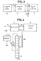
- FIG. 3 we can see an example of a BILBO type test device.
- the inputs of the device to be tested for example an integrated circuit, are connected to the outputs 4 of the test vector generator 10, for example analogous to the test vector generator illustrated in FIG. 1.
- the outputs of the device to be tested are connected to the inputs 5 of the signature analysis device.
- the signature analysis device 1 is for example analogous to the device illustrated in FIG. 2.
- the outputs 5 can be read outside allowing the reading at the end of the test of the values contained in the shift register 2.
- the device to be tested 6 is normally connected to an external input / output bus. 146.
- the bus 146 is connected to a multiplexer 7.
- the multiplexer 7 is connected to the device to be tested 6 via a bus 147, and to a test 11 by a bus 145.
- the test device 11 includes a shift register 2, certain cells of which are looped back through an OR-exclusive gate 3 at its input. The cells of the shift register 2 can be read and written in parallel via the bus 145.
- the multiplexer 7 makes it possible either to connect the bus 146 to the bus 147, or to connect the bus 145 to the bus 147.
- the multiplexer 7 comprises, for example three-state devices (three state in English terminology).
- the shift register 2 is initialized, for example all the cells of the shift register 2 have the value 1.
- the test device 11 transmits via the bus 145 of the multiplexer 7 and the bus 147 to the inputs of the device to be tested 6 of the test vectors.
- the shift register 2 of the test device 11 receives via the bus 147, the multiplexer 7 and the bus 145 the values of the outputs generated in response to the test vectors by the device to be tested 6.
- test result is read either by a 3N serial bus connected to the last output of the shift register 2 or, advantageously by via bus 145 of multiplexer 7 and bus 146.
- the control device 8 makes it possible to control the multiplexer 7.
- the bus 146 is connected by the multiplexer 7 to the bus 147.
- the test device 11 is perfectly transparent to the user.
- the control device 8 performs the necessary switches.
- the control devices 8 include counters making it possible to measure the number of cycles carried out.
- the control device 8 includes a logic circuit making it possible to automate the test. The test carried out either periodically or on command 149 of the control device 8.
- the test device is integrated into the device to be tested.
- the device to be tested 6 is an integrated circuit carrying out the fast Fourier transform (FFT in English terminology).
- the external input / output bus 146 is connected to the internal input / output bus 153.
- the internal input / output bus 153 is connected to the multiplexer 7.
- the multiplexer 7 is connected on the one hand to the bus 154 and d on the other hand to the bus 152.
- the bus 154 is a bidirectional bus connecting the multiplexer 7 to the test device 11.
- the test device 11 is connected to an internal bus 155.
- the bus 152 is for example the internal output bus of the device to be tested 6.
- the internal output bus 151 is connected to a register 9, itself connected to the bus 152.
- a control device 8 is connected by a bus 148 to the multiplexer 7.
- the multiplexer 7 makes it possible either to connect via bus 153 and 154 the bus 146 to the bus 155, or to connect, via the bus 152 and 154 the bus 151 to the test device 11.
- the first case corresponds to the normal operation of the device to be tested 6.
- the second corresponds to the test of the device to be tested 6.
- the multiplexer 7 makes it possible to route the signals from bus 152 to bus 154, without however isolating bus 154 from bus 153 connected to bus 146.
- any bonding to 0 or 1 gives bits of the bus 146 or of the bus 153 modifying the content of the register 2 of the test device 11. This sticking to 0 or to 1 will therefore be detected as a malfunction of the device to be tested 6.
- the invention mainly applies to the testing of electrical circuits, in particular digital and / or logic circuits.
- the invention applies in particular to the testing of integrated circuits, printed circuits, and of any device using signal processing.
- the invention is particularly applicable to the testing of computers, microprocessors, memories, fast Fourier transform computers, adders, multipliers, combinatorial logics, as well as combinatorial logics comprising internal storage devices.
Abstract
L'invention a principalement pour objet un dispositif de test de circuit électrique et un circuit comportant ledit dispositif. L'invention concerne principalement un dispositif de test des circuits électriques par génération de vecteurs de tests et compression du signal en sortie du dispositif à tester. Le dispositif selon la présente invention utilise le même registre à décalage (2) dont certaines cellules sont bouclées sur l'entrée par l'intermédiaire d'une logique OU-exclusif (3) pour effectuer la génération des vecteurs de test et l'analyse des signatures. Ainsi il est possible d'effectuer le test de circuits électriques eux-mêmes ainsi que les bus d'entrée/sortie. L'invention s'applique notamment aux tests des calculateurs, des microprocesseurs, des mémoires, des calculateurs de transformée de Fourier rapide, des additionneurs, des multiplieurs, des logiques combinatoires, ainsi que des logiques combinatoires comportant des dispositifs de mémorisation interne.The main object of the invention is an electrical circuit test device and a circuit comprising said device. The invention relates mainly to a device for testing electrical circuits by generating test vectors and compressing the signal at the output of the device to be tested. The device according to the present invention uses the same shift register (2) of which certain cells are looped over the input via an OR-exclusive logic (3) to carry out the generation of the test vectors and the analysis signatures. Thus it is possible to perform the test of the electrical circuits themselves as well as the input / output buses. The invention is particularly applicable to the testing of computers, microprocessors, memories, fast Fourier transform computers, adders, multipliers, combinatorial logics, as well as combinatorial logics comprising internal storage devices.
Description
La présente invention a principalement pour objet un dispositif de test de circuit électrique et un circuit comportant ledit dispositif.The main object of the present invention is an electrical circuit test device and a circuit comprising said device.
La présente invention se rapporte principalement aux tests de bon fonctionnement de circuits électriques comme par exemple des circuits numériques et/ou logiques. Elle permet de détecter le mauvais fonctionnement d'un circuit intégré, circuit imprimé ou de tout autre dispositif électronique. Une fois la panne détectée, il est possible, de prendre les mesures permettant de minimiser les conséquences de cette panne. Par exemple, on remplace le circuit électrique défaillant, ou l'on ne tient pas compte du résultat fourni par ledit circuit.The present invention mainly relates to tests of the proper functioning of electrical circuits such as, for example, digital and / or logic circuits. It can detect the malfunction of an integrated circuit, printed circuit or any other electronic device. Once the failure has been detected, it is possible to take measures to minimize the consequences of this failure. For example, the faulty electrical circuit is replaced, or the result supplied by said circuit is not taken into account.
L'augmentation de complexité des circuits électroniques rend de plus en plus difficile un test exhaustif de ces circuits, détectant à coup sûr toute panne. Il est connu des méthodes permettant un test ayant de très grandes chances de détecter une panne dans un circuit. Notamment, il est connu d'injecter dans le circuit numérique et/ou logique des suites de vecteurs pseudo-aléatoires longues. Les suites pseudo-aléatoires longues sont obtenues en rebouclant certaines cellules d'un registre à décalage à travers une porte OU-exclusif. En utilisant des polynomes générateurs de degré N il est possible d'obtenir des suites ayant une longueur 2N - 1.The increasing complexity of electronic circuits makes it more and more difficult to exhaustively test these circuits, surely detecting any failure. Methods are known which allow a test with very high chances of detecting a fault in a circuit. In particular, it is known to inject into the digital and / or logic circuit sequences of long pseudo-random vectors. Long pseudo-random sequences are obtained by looping certain cells of a shift register through an OR-exclusive gate. By using generator polynomials of degree N it is possible to obtain sequences having a length 2 N - 1.
A la sortie du dispositif à tester il suffit de vérifier la conformité des résultats obtenus avec ceux qui devraient être fournis par une carte en bon état de fonctionnement. Par exemple on compare le résultat obtenu avec ceux fournis par une carte que l'on sait fonctionner parfaitement, ou alors avec des résultats que l'on a obtenu par simulation.On leaving the device to be tested, it suffices to check the conformity of the results obtained with those which should be supplied by a card in good working order. For example, we compare the result obtained with those provided by a card that we know to work perfectly, or with results that we obtained by simulation.
Une méthode plus perfectionnée consiste à utiliser l'analyse des signatures. Cette méthode est connue sous le nom de méthode BILBO. A la sortie du dispositif à tester on connecte un autre registre à décalage dont certaines cellules sont rebouclées à travers une porte OU-exclusif. Ce second registre à décalage muni de sa porte logique OU-exclusif permet de comprimer les informations obtenues. A la fin du test il suffit de comparer le contenu du registre à décalage avec celui qui devrait être obtenu, pour un dispositif en parfait état de fonctionnement, pour détecter, avec une très grande efficacité, si le dispositif testé est en panne ou non.A more sophisticated method is to use signature analysis. This method is known as the BILBO method. At the output of the device to be tested, connect another shift register some cells of which are looped through an OR-exclusive gate. This second shift register provided with its OR-exclusive logic gate makes it possible to compress the information obtained. At the end of the test, it suffices to compare the content of the shift register with that which should be obtained, for a device in perfect working order, to detect, with very high efficiency, whether the device tested is faulty or not.
Le dispositif de type connu présente l'inconvénient de ne pas effectuer les tests de bus d'entrée/sortie du dispositif.The known type of device has the disadvantage of not performing the input / output bus tests of the device.
Le dispositif objet de la présente invention utilise un registre à décalage unique bouclé à travers, une porte logique OU-exclusif pour effectuer la génération des vecteurs de test ainsi que la compression d'information. Ce dispositif est connecté au bus d'entrée/sortie du système à tester. Ainsi il permet de détecter des collages à 0 ou des collages à 1 sur ce bus. Par contre il ne permet pas de détecter des coupures de bus. Le dispositif selon la présente invention comporte un multiplexeur permettant d'envoyer vers le registre à décalage les informations présentes à la sortie du dispositif à tester.The device object of the present invention uses a single shift register looped through, an OR-exclusive logic gate to perform the generation of test vectors as well as information compression. This device is connected to the input / output bus of the system to be tested. Thus it makes it possible to detect collages at 0 or collages at 1 on this bus. By cons it does not detect bus outages. The device according to the present invention comprises a multiplexer making it possible to send the information present at the output of the device to be tested to the shift register.
De plus, l'utilisation d'un registre à décalage unique pour la génération de vecteurs de test et pour la compression des réponses fournies par le dispositif à tester permet de réduire la quantité de matériel nécessaire à la réalisation du test. Cette réduction sera particulièrement importante par rapport au matériel total dans le cas de dispositif de test inclus dans des circuits intégrés.In addition, the use of a single shift register for the generation of test vectors and for the compression of the responses provided by the device to be tested makes it possible to reduce the amount of material necessary for carrying out the test. This reduction will be particularly significant compared to the total material in the case of test device included in integrated circuits.
L'utilisation d'un même registre à décalage pour la génération des vecteurs de tests et pour la compression des informations entraîne la modification du contenu du registre à décalage entre la génération de deux vecteurs des tests successifs, par rapport à leur contenu dans le fonctionnement du générateur de tests de type connu. A priori on pourrait s'attendre à une très importante diminution de l'efficacité des tests, c'est-à-dire du nombre de pannes détectées par rapport au nombre de pannes réelles. L'expérimentation a permis de prouver qu'il était possible d'obtenir une effica cité supérieure à 99%, par exemple 99,6%.The use of the same shift register for the generation of test vectors and for the compression of information results in the modification of the content of the shift register between the generation of two vectors of successive tests, with respect to their content in operation. of the known type test generator. A priori one could expect a very significant reduction in the efficiency of the tests, that is to say the number of failures detected compared to the number of actual failures. Experimentation has proven that it was possible to obtain an effica cited above 99%, for example 99.6%.
Dans une variante de réalisation du dispositif selon la présente invention le dispositif de test est inclus dans le dispositif à tester, par exemple, un circuit intégré ou un circuit imprimé.In an alternative embodiment of the device according to the present invention, the test device is included in the device to be tested, for example, an integrated circuit or a printed circuit.
Dans une deuxième variante de réalisation du dispositif selon la présente invention il est commun à un ensemble d'équipement. Il est possible de réaliser le test d'un équipement particulier en le branchant sur un bus entrée/sortie commun.In a second variant embodiment of the device according to the present invention, it is common to a set of equipment. It is possible to test a particular piece of equipment by connecting it to a common input / output bus.
Dans une troisième variante de réalisation le dispositif de test selon la présente invention est autonome. Il est possible de le brancher sur un quelconque équipement pour en effectuer le test.In a third variant embodiment, the test device according to the present invention is autonomous. It is possible to connect it to any equipment to carry out the test.
L'invention a principalement pour objet un dispositif de test pour circuit électrique et notamment pour circuits numériques et/ou logiques comportant un registre à décalage dont au moins une cellule est reliée aux entrées d'une porte logique OU-exclusif, la sortie de ladite porte logique OU-exclusif étant connectée sur l'entrée dudit registre à décalage, caractérisé par le fait que le registre à décalage est susceptible d'être connecté à l'entrée du dispositif à tester pour générer des vecteurs de test et à la sortie du dispositif à tester pour comprimer les informations disponibles en sortie de façon à permettre d'effectuer l'analyse de signature dudit dispositif à tester.The invention mainly relates to a test device for an electrical circuit and in particular for digital and / or logic circuits comprising a shift register of which at least one cell is connected to the inputs of an OR-exclusive logic gate, the output of said OU-exclusive logic gate being connected to the input of said shift register, characterized in that the shift register is capable of being connected to the input of the device to be tested to generate test vectors and to the output of the device to be tested to compress the information available at the output so as to allow the signature analysis of said device to be tested.
L'invention sera mieux comprise au moyen de la description ci-après et des figures données comme des exemples non limitatifs parmi lesquels :
- - la figure 1 est un schéma d'un générateur de vecteur de test de type connu ;
- - la figure 2 est un schéma d'un dispositif de compression d"information de type connu ;
- - la figure 3 est un schéma d'un dispositif de test de type BILBO ;
- - la figure 4 est un schéma d'un premier exemple de réalisation du dispositif selon la présente invention ;
- - la figure 5 est un schéma d'un second exemple de réalisation du dispositif selon la présente invention.
- - Figure 1 is a diagram of a test vector generator of known type;
- - Figure 2 is a diagram of an information compression device of known type;
- - Figure 3 is a diagram of a BILBO type test device;
- - Figure 4 is a diagram of a first embodiment of the device according to the present invention;
- - Figure 5 is a diagram of a second embodiment of the device according to the present invention.
Sur les figures 1 à 5 on a utilisé les mêmes références pour désiger les mêmes éléments.In FIGS. 1 to 5, the same references have been used to designate the same elements.
Sur la figure 1, on peut voir le principe d'un générateur 10 de signaux pseudo-aléatoires. Ledit générateur comporte un registre à décalage 2 comportant M cellules référencées 20 à 2(M-1), et une porte logique OU-exclusif 3. Le registre à décalage 2 décale, à chaque impulsion d'horloge (non illustrée) l'information présente dans une cellule dans le sens des références croissantes. Ainsi après M cycles d'horloge une information présentée à l'entrée de la cellule 20 est présente à la sortie de la cellule 2(M-1). La cellule 2(M-1) est reliée à une des entrées de la porte logique OU-exclusif 3 par une ligne 3M. La sortie de la porte logique OU-exclusif 3 est reliée par une ligne 30 à la cellule 20. Certaines cellules du registre à décalage 2 sont reliées à des entrées de la porte logique OU-exclusif 3. Dans l'exemple, du registre illustré sur la figure 1 la cellule 21 est reliée par la ligne 31 à une entrée de la porte logique OU-exclusif 3, la cellule 22 est reliée par la ligne 32 à une entrée de la porte logique OU-exclusif 3 ainsi que la cellule 25 est reliée par la ligne 35 à une entrée de la porte logique OU-exclusif 3.In Figure 1, we can see the principle of a
Le tableau I donne les puissances non triviales de polynomes générateurs permettant pour un registre à décalage comportant M cellules d'obtenir 2M-1 mots de M bits différents.

Ainsi si par exemple nous voulons utiliser le polynome générateur de degré 27 :
P₂₇ (X) = X²⁷ + X⁵ + X² + X + 1
nous allons utiliser un registre à décalage 1 comportant 27 cellules.So if for example we want to use the generator polynomial of degree 27:
P₂₇ (X) = X²⁷ + X⁵ + X² + X + 1
we're going to use a
Dans ce cas en plus de la première cellule 2(M-1) toujours bouclée sur une entrée de la porte logique OU-exclusif 3 nous rebouclerons la seconde, la troisième et la sixième cellules référencées respectivement 21, 22 et 25 sur la figure 1.In this case in addition to the first cell 2 (M-1) always looped on an input of the OR-
Les mots de M bits sont disponibles sur les sorties 4 du registre à décalage 2. Dans l'exemple illustré sur la figure 1 les sorties du registre à déclage 2 sont référencées 40 à 4(M-1).The words of M bits are available on the
Sur la figure 2, on peut voir le principe d'un dispositif de compression d'information utilisé pour l'analyse des signaux pour test de circuit électrique.In Figure 2, we can see the principle of an information compression device used for the analysis of signals for electrical circuit test.
Le dispositif illustré sur la figure 2 comporte un registre à décalage de N cellules référencé 20 à 2(N-1) et une porte logique OU-exclusif 3. Le registre à décalage 2 décale à chaque impulsion d'horloge (non illustrée) l'information présente dans une des cellules dans un sens de référence croissant et modifiée par une fonction OU-exclusif par le signal 5 correspondant. La cellule 2(N-1) est reliée à une des entrées de la porte logique OU-exclusif 3 par une ligne 3N. La sortie de la porte logique OU-exclusif 3 est reliée par une ligne 30 à la cellule 20. Certaines cellules du registre à décalage 2 sont reliées à des entrées de la porte logique OU-exclusif 3. Dans l'exemple illustré sur la figure 2, la cellule 21 est reliée par la ligne 31 à une entrée de la porte OU-exclusif 3, la cellule 22 est reliée par la ligne 32 à une entrée de la porte logique OU-exclusif 3, ainsi que la cellule 25 est reliée par la ligne 35 à l'entrée de la porte logique OU-exclusif 3.The device illustrated in FIG. 2 comprises a register with shift of N cells referenced 20 to 2 (N-1) and an OR-
Les données à compresser sont rentrées dans un registre à décalage 2 par l'intermédiaire des entrées 5. Sur la figure 2 les entrées 5 correspondant aux cellules 20 à 2(N-1) sont référencées 50 à 5(N-1). Le résultat de la compression est lu soit par l'intermédiaire des entrées 5, en parallèle, soit en série par l'intermédiaire de la ligne 3N reliée à la dernière cellule du registre à décalage 2, 2(N-1).The data to be compressed are entered in a
Sur la figure 3, on peut voir un exemple de dispositif de test de type BILBO. Les entrées du dispositif à tester, par exemple un circuit intégré sont reliés aux sorties 4 du générateur de vecteur de test 10, par exemple analogue au générateur de vecteur de test illustré sur la figure 1.In Figure 3, we can see an example of a BILBO type test device. The inputs of the device to be tested, for example an integrated circuit, are connected to the
Les sorties du dispositif à tester sont reliées aux entrées 5 du dispositif d'analyse de signature. Le dispositif d'analyse de signature 1 est par exemple analogue au dispositif illustré sur la figure 2. Dans l'exemple illustré sur la figure 3 les sorties 5 sont susceptibles d'être lues à l'extérieur permettant la lecture en fin de test des valeurs contenues par le registre à décalage 2.The outputs of the device to be tested are connected to the
Sur la figure 4, on peut voir un exemple de réalisation du dispositif selon l'invention. Dans l'exemple de la figure 4 le dispositif à tester 6 est normalement relié à un bus d'entrée/sortie externe 146. Pour pouvoir à tout moment réaliser les tests du dispositif à tester 6 le bus 146 est relié à un multiplexeur 7. Le multiplexeur 7 est relié au dispositif à tester 6 par l'intermédiaire d'un bus 147, et à un dispositif de test 11 par un bus 145. Le dispositif de test 11 comporte un registre à décalage 2 dont certaines cellules sont rebouclées par une porte OU-exclusif 3 à son entrée. Les cellules du registre à décalage 2 sont susceptibles d'être lues et écrites en parallèle par l'intermédiaire du bus 145.In Figure 4, we can see an embodiment of the device according to the invention. In the example of FIG. 4, the device to be tested 6 is normally connected to an external input / output bus. 146. In order to be able to carry out the tests of the device to be tested at any time, the
Le multiplexeur 7 permet soit de relier le bus 146 au bus 147, soit de relier le bus 145 au bus 147. Le multiplexeur 7 comporte par exemple des dispositifs trois états (three state en terminologie anglo-saxonne).The
Au premier cycle d'horloge le registre à décalage 2 est initialisé, par exemple toutes les cellules du registre à décalage 2 comportent la valeur 1. A un cycle horloge sur deux, par exemple pendant les cycles d'horloge pairs le dispositif de test 11 transmet par l'intermédiaire du bus 145 du multiplexeur 7 et du bus 147 aux entrées du dispositif à tester 6 des vecteurs de test. Pendant les cycles d'horloge complémentaires c'est-à-dire dans notre exemple pendant le cycle d'horloge impair le registre à décalage 2 du dispositif de test 11 reçoit par l'intermédiaire du bus 147, du multiplexeur 7 et du bus 145 les valeurs des sorties générées en réponse aux vecteurs de tests par le dispositif à tester 6.At the first clock cycle the
Ainsi, les vecteurs de tests générés par le dispositif 11 sont les réponses modifiées aux vecteurs de tests précédents du dispositif 6. Il à noter que le dispositif 11 ne va plus générer 2N vecteurs différents de N bits pour le test. Néanmoins dans la plupart des cas il a été vérifié expérimentalement que l'on obtient un test quasi exhaustif. Il a été notamment vérifié pour les polynomes générateurs F(X) = X³³ + X¹³ + 1 et pour le polynome X⁴⁷ +1. Ce polynome présente en plus l'avantage de nécessiter peu de connexion au niveau de la porte logique OU-exclusif 3.Thus, the test vectors generated by the
Le résultat du test est lu soit par un bus série 3N connecté à la dernière sortie du registre à décalage 2 soit, avantageusement par l'intermédiaire du bus 145 du multiplexeur 7 et du bus 146.The test result is read either by a 3N serial bus connected to the last output of the
Le dispositif de commande 8 permet de commander le multiplexeur 7.The
En dehors des périodes de test le bus 146 est relié par le multiplexeur 7 au bus 147. Le dispositif de test 11 est parfaitement transparent à l'utilisateur. Dans la période de test le dispositif de commande 8 effectue les commutations nécessaires. Par exemple, les dispositifs de commande 8 comportent des compteurs permettant de mesurer le nombre de cycles effectués. Avantageusement le dispositif de commande 8 comporte un circuit logique permettant d'automatiser le test. Le test effectué soit périodiquement, soit sur commande 149 du dispositif de commande 8.Outside of the test periods, the
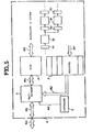
Sur la figure 5, on peut voir un second exemple de réalisation du dispositif selon l'invention. Dans l'exemple illustré sur la figure 5, le dispositif de test est intégré au dispositif à tester. Par exemple le dispositif à tester 6 est un circuit intégré réalisant la transformée de Fourier rapide (FFT en terminologie anglo-saxonne). Le bus externe d'entrée/sortie 146 est relié au bus interne d'entrée/sortie 153. Le bus interne d'entrée/sortie 153 est relié au multiplexeur 7. Le multiplexeur 7 est relié d'une part au bus 154 et d'autre part au bus 152. Le bus 154 est un bus bidirectionnel reliant le multiplexeur 7 au dispositif de test 11. Le dispositif de test 11 est relié à un bus interne 155.In Figure 5, we can see a second embodiment of the device according to the invention. In the example illustrated in FIG. 5, the test device is integrated into the device to be tested. For example, the device to be tested 6 is an integrated circuit carrying out the fast Fourier transform (FFT in English terminology). The external input /
Le bus 152 est par exemple le bus de sortie interne du dispositif à tester 6. Avantageusement, le bus de sortie interne 151 est relié à un registre 9, lui-même relié au bus 152.The
Un dispositif de commande 8 est relié par un bus 148 au multiplexeur 7.A
Le multiplexeur 7 permet soit de relier par l'intermédiaire de bus 153 et 154 le bus 146 au bus 155, soit de relier, par l'intermédiaire de bus 152 et 154 le bus 151 au dispositif de test 11. Le premier cas correspond au fonctionnement normal du dispositif à tester 6. Dans ce cas, il est avantageux d'utiliser le registre à décalage 2 du dispositif de test 11 comme registre tampon d'entrée/sortie du dispositif à tester 6.The
Le second correspond au test du dispositif à tester 6.The second corresponds to the test of the device to be tested 6.
Dans une variante particulièrement avantageuse de l'invention le multiplexeur 7 permet d'aiguiller les signaux du bus 152 vers le bus 154, sans pour autant isoler le bus 154 du bus 153 relié au bus 146. Ainsi, tout collage à 0 ou à 1 donne des bits du bus 146 ou du bus 153 modifiant le contenu du registre 2 du dispositif du test 11. Ce collage à 0 ou à 1 va donc être détecté comme une faute de fonctionnement du dispositif à tester 6.In a particularly advantageous variant of the invention, the
L'invention s'applique principalement au test de circuit électrique, notamment des circuits numériques et/ou logiques.The invention mainly applies to the testing of electrical circuits, in particular digital and / or logic circuits.
L'invention s'applique notamment aux tests des circuits intégrés, des circuits imprimés, et de tout dispositif utilisant le traitement du signal.The invention applies in particular to the testing of integrated circuits, printed circuits, and of any device using signal processing.
L'invention s'applique particulièrement aux tests des calculateurs, des microprocesseurs, des mémoires, des calculateurs de transformée de Fourier rapide, des additionneurs, des multiplieurs, des logiques combinatoires, ainsi que des logiques combinatoires comportant des dispositifs de mémorisation interne.The invention is particularly applicable to the testing of computers, microprocessors, memories, fast Fourier transform computers, adders, multipliers, combinatorial logics, as well as combinatorial logics comprising internal storage devices.
Claims (10)
Applications Claiming Priority (2)
| Application Number | Priority Date | Filing Date | Title |
|---|---|---|---|
| FR8702003 | 1987-02-17 | ||
| FR8702003A FR2611052B1 (en) | 1987-02-17 | 1987-02-17 | ELECTRICAL CIRCUIT TEST DEVICE AND CIRCUIT COMPRISING SAID DEVICE |
Publications (1)
| Publication Number | Publication Date |
|---|---|
| EP0279738A1 true EP0279738A1 (en) | 1988-08-24 |
Family
ID=9347998
Family Applications (1)
| Application Number | Title | Priority Date | Filing Date |
|---|---|---|---|
| EP88400318A Withdrawn EP0279738A1 (en) | 1987-02-17 | 1988-02-12 | Electrical circuit testing device, and circuit containing the same |
Country Status (3)
| Country | Link |
|---|---|
| US (1) | US4982403A (en) |
| EP (1) | EP0279738A1 (en) |
| FR (1) | FR2611052B1 (en) |
Cited By (1)
| Publication number | Priority date | Publication date | Assignee | Title |
|---|---|---|---|---|
| WO1992013281A1 (en) * | 1991-01-22 | 1992-08-06 | Vlsi Technology, Inc. | Method to reduce test vectors/test time in devices using equivalent blocks |
Families Citing this family (6)
| Publication number | Priority date | Publication date | Assignee | Title |
|---|---|---|---|---|
| US5412580A (en) * | 1991-07-03 | 1995-05-02 | Hughes Aircraft Company | Pseudo-random vector generated testable counter |
| US5258985A (en) * | 1991-11-12 | 1993-11-02 | Motorola, Inc. | Combinational data generator and analyzer for built-in self test |
| DE59915081D1 (en) * | 1998-06-16 | 2009-10-22 | Infineon Technologies Ag | Device for measuring and analyzing electrical signals of an integrated circuit module |
| US20060031672A1 (en) * | 2004-08-03 | 2006-02-09 | Soltis Donald C Jr | Resource protection in a computer system with direct hardware resource access |
| US7930539B2 (en) * | 2004-08-03 | 2011-04-19 | Hewlett-Packard Development Company, L.P. | Computer system resource access control |
| US20060112257A1 (en) * | 2004-11-12 | 2006-05-25 | Undy Stephen R | Microprocessor architected state signature analysis |
Citations (2)
| Publication number | Priority date | Publication date | Assignee | Title |
|---|---|---|---|---|
| EP0037965A2 (en) * | 1980-04-11 | 1981-10-21 | Siemens Aktiengesellschaft | Device for testing a digital circuit with test circuits enclosed in this circuit |
| US4571724A (en) * | 1983-03-23 | 1986-02-18 | Data I/O Corporation | System for testing digital logic devices |
Family Cites Families (7)
| Publication number | Priority date | Publication date | Assignee | Title |
|---|---|---|---|---|
| US4513418A (en) * | 1982-11-08 | 1985-04-23 | International Business Machines Corporation | Simultaneous self-testing system |
| US4601034A (en) * | 1984-03-30 | 1986-07-15 | Texas Instruments Incorporated | Method and apparatus for testing very large scale integrated memory circuits |
| US4779273A (en) * | 1984-06-14 | 1988-10-18 | Data General Corporation | Apparatus for self-testing a digital logic circuit |
| GB8432533D0 (en) * | 1984-12-21 | 1985-02-06 | Plessey Co Plc | Integrated circuits |
| GB8432458D0 (en) * | 1984-12-21 | 1985-02-06 | Plessey Co Plc | Integrated circuits |
| EP0196171B1 (en) * | 1985-03-23 | 1991-11-06 | International Computers Limited | Digital integrated circuits |
| US4703484A (en) * | 1985-12-19 | 1987-10-27 | Harris Corporation | Programmable integrated circuit fault detection apparatus |
-
1987
- 1987-02-17 FR FR8702003A patent/FR2611052B1/en not_active Expired
-
1988
- 1988-02-12 EP EP88400318A patent/EP0279738A1/en not_active Withdrawn
-
1990
- 1990-03-01 US US07/490,510 patent/US4982403A/en not_active Expired - Fee Related
Patent Citations (2)
| Publication number | Priority date | Publication date | Assignee | Title |
|---|---|---|---|---|
| EP0037965A2 (en) * | 1980-04-11 | 1981-10-21 | Siemens Aktiengesellschaft | Device for testing a digital circuit with test circuits enclosed in this circuit |
| US4571724A (en) * | 1983-03-23 | 1986-02-18 | Data I/O Corporation | System for testing digital logic devices |
Non-Patent Citations (3)
| Title |
|---|
| IBM TECHNICAL DISCLOSURE BULLETIN, vol. 25, no. 10, mars 1983, pages 4958-4960, New York, US; P.S. BOTTORFF et al.: "Self-testing scheme using shift register latches" * |
| IBM TECHNICAL DISCLOSURE BULLETIN, vol. 26, no. 10B, mars 1984, pages 5566-5570, New York, US; A. BLUM: "Self-testing mechanism" * |
| IBM TECHNICAL DISCLOSURE BULLETIN, vol. 26, no. 3B, août 1983, pages 1604-1606, New York, US; D.A. CALVIN: "Design for self-test SRL implementation" * |
Cited By (2)
| Publication number | Priority date | Publication date | Assignee | Title |
|---|---|---|---|---|
| WO1992013281A1 (en) * | 1991-01-22 | 1992-08-06 | Vlsi Technology, Inc. | Method to reduce test vectors/test time in devices using equivalent blocks |
| US5412313A (en) * | 1991-01-22 | 1995-05-02 | Vlsi Technology, Inc. | Method to reduce test vectors/test time in devices using equivalent blocks |
Also Published As
| Publication number | Publication date |
|---|---|
| FR2611052A1 (en) | 1988-08-19 |
| US4982403A (en) | 1991-01-01 |
| FR2611052B1 (en) | 1989-05-26 |
Similar Documents
| Publication | Publication Date | Title |
|---|---|---|
| FR2483713A1 (en) | DEVICE FOR TRANSMITTING SIGNALS BETWEEN TWO INFORMATION PROCESSING STATIONS | |
| FR2960978A1 (en) | ASYNCHRONOUS SEQUENCE COMPARATOR FOR INTEGRATED SELF-TEST CIRCUIT | |
| FR2960977A1 (en) | VARIABLE SOLICITATION SEQUENCE GENERATOR FOR INTEGRATED SELF-TEST CIRCUIT | |
| FR3038752A1 (en) | ||
| EP0279738A1 (en) | Electrical circuit testing device, and circuit containing the same | |
| FR2693574A1 (en) | Method for testing the operation of a specialized integrated circuit, and specialized integrated circuit relating thereto. | |
| EP0166838B1 (en) | Method and arrangement for detecting a particular bit configuration in a serial bit stream | |
| CN109558331A (en) | Defect inspection method, device, equipment and the storage medium of application program | |
| EP0543698B1 (en) | Device for employment of fault information in a single/multi-computer aircraft system | |
| FR2610430A1 (en) | CONTACTLESS READ TYPE INTEGRATED CIRCUIT CARD WITH PRE-IMPROVEMENT FUNCTION | |
| FR2903497A1 (en) | ELECTRONIC CIRCUIT COMPRISING A SECURE TEST MODE BY INSERTING LURE DATA IN THE TEST CHAIN, AND ASSOCIATED METHOD. | |
| FR2911973A1 (en) | COMMUNICATION GATEWAY BETWEEN TWO ENTITIES | |
| CH659721A5 (en) | APPARATUS FOR EXAMINING AN INTERNAL INTERCONNECTION CIRCUIT BETWEEN N TERMINALS OF AN ELECTRICAL NETWORK AND USE OF THIS APPARATUS. | |
| EP0344052B1 (en) | Modular memory | |
| JP2022177708A (en) | Device and program for detecting deterioration | |
| EP1051693B1 (en) | Asynchronous memory card | |
| FR2664114A1 (en) | INTERFACE MODULE FOR TRANSFERRING DATA. | |
| EP1554653B1 (en) | Repeat digital message transmission between a microprocessor monitoring circuit and an analyzing tool | |
| EP0190514A1 (en) | On-line test device of the discrete Fourier transform calculating circuit, and circuit using such a device | |
| EP0635786A1 (en) | Device for storing data | |
| FR2948473A1 (en) | INTERFACE CIRCUIT COMPRISING A MEMORY OF FIFO TYPE | |
| FR2490367A1 (en) | COUPLER OF REMOVABLE ELECTRONIC SUPPORTS | |
| FR3078416A1 (en) | MEASURING DEVICE FOR MEASURING THE LATENCY TIME OF PROCESSING A COMPUTER SYSTEM, METHOD OF USING THE SAME | |
| EP0675438B1 (en) | Method and device for error detection on electronic boards | |
| EP0343083B1 (en) | Loss of synchronisation detection device, and its use in a digital transmission network |
Legal Events
| Date | Code | Title | Description |
|---|---|---|---|
| PUAI | Public reference made under article 153(3) epc to a published international application that has entered the european phase |
Free format text: ORIGINAL CODE: 0009012 |
|
| AK | Designated contracting states |
Kind code of ref document: A1 Designated state(s): DE GB IT NL |
|
| 17P | Request for examination filed |
Effective date: 19890201 |
|
| RAP3 | Party data changed (applicant data changed or rights of an application transferred) |
Owner name: THOMSON-CSF |
|
| 17Q | First examination report despatched |
Effective date: 19910208 |
|
| STAA | Information on the status of an ep patent application or granted ep patent |
Free format text: STATUS: THE APPLICATION IS DEEMED TO BE WITHDRAWN |
|
| 18D | Application deemed to be withdrawn |
Effective date: 19920630 |