EP0287311A2 - Duty cycle independent phase detector - Google Patents

Duty cycle independent phase detector Download PDF

Info

Publication number
EP0287311A2
EP0287311A2 EP88303238A EP88303238A EP0287311A2 EP 0287311 A2 EP0287311 A2 EP 0287311A2 EP 88303238 A EP88303238 A EP 88303238A EP 88303238 A EP88303238 A EP 88303238A EP 0287311 A2 EP0287311 A2 EP 0287311A2
Authority
EP
European Patent Office
Prior art keywords
circuit
signal
input
output
phase
Prior art date
Legal status (The legal status is an assumption and is not a legal conclusion. Google has not performed a legal analysis and makes no representation as to the accuracy of the status listed.)
Withdrawn
Application number
EP88303238A
Other languages
German (de)
French (fr)
Other versions
EP0287311A3 (en
Inventor
Roger Dean Thornton
Current Assignee (The listed assignees may be inaccurate. Google has not performed a legal analysis and makes no representation or warranty as to the accuracy of the list.)
Sundstrand Corp
Original Assignee
Sundstrand Corp
Westinghouse Electric Corp
Priority date (The priority date is an assumption and is not a legal conclusion. Google has not performed a legal analysis and makes no representation as to the accuracy of the date listed.)
Filing date
Publication date
Application filed by Sundstrand Corp, Westinghouse Electric Corp filed Critical Sundstrand Corp
Publication of EP0287311A2 publication Critical patent/EP0287311A2/en
Publication of EP0287311A3 publication Critical patent/EP0287311A3/en
Withdrawn legal-status Critical Current

Links

Images

Classifications

    • HELECTRICITY
    • H03ELECTRONIC CIRCUITRY
    • H03LAUTOMATIC CONTROL, STARTING, SYNCHRONISATION, OR STABILISATION OF GENERATORS OF ELECTRONIC OSCILLATIONS OR PULSES
    • H03L7/00Automatic control of frequency or phase; Synchronisation
    • H03L7/06Automatic control of frequency or phase; Synchronisation using a reference signal applied to a frequency- or phase-locked loop
    • H03L7/08Details of the phase-locked loop
    • HELECTRICITY
    • H03ELECTRONIC CIRCUITRY
    • H03DDEMODULATION OR TRANSFERENCE OF MODULATION FROM ONE CARRIER TO ANOTHER
    • H03D13/00Circuits for comparing the phase or frequency of two mutually-independent oscillations
    • H03D13/003Circuits for comparing the phase or frequency of two mutually-independent oscillations in which both oscillations are converted by logic means into pulses which are applied to filtering or integrating means
    • H03D13/004Circuits for comparing the phase or frequency of two mutually-independent oscillations in which both oscillations are converted by logic means into pulses which are applied to filtering or integrating means the logic means delivering pulses at more than one terminal, e.g. up and down pulses
    • HELECTRICITY
    • H03ELECTRONIC CIRCUITRY
    • H03LAUTOMATIC CONTROL, STARTING, SYNCHRONISATION, OR STABILISATION OF GENERATORS OF ELECTRONIC OSCILLATIONS OR PULSES
    • H03L7/00Automatic control of frequency or phase; Synchronisation
    • H03L7/06Automatic control of frequency or phase; Synchronisation using a reference signal applied to a frequency- or phase-locked loop
    • H03L7/08Details of the phase-locked loop
    • H03L7/085Details of the phase-locked loop concerning mainly the frequency- or phase-detection arrangement including the filtering or amplification of its output signal
    • H03L7/089Details of the phase-locked loop concerning mainly the frequency- or phase-detection arrangement including the filtering or amplification of its output signal the phase or frequency detector generating up-down pulses
    • HELECTRICITY
    • H04ELECTRIC COMMUNICATION TECHNIQUE
    • H04LTRANSMISSION OF DIGITAL INFORMATION, e.g. TELEGRAPHIC COMMUNICATION
    • H04L7/00Arrangements for synchronising receiver with transmitter
    • H04L7/02Speed or phase control by the received code signals, the signals containing no special synchronisation information
    • H04L7/033Speed or phase control by the received code signals, the signals containing no special synchronisation information using the transitions of the received signal to control the phase of the synchronising-signal-generating means, e.g. using a phase-locked loop

Abstract

A duty cycle independent phase detecting circuit (10) for use in phase-locked loops is provided with a pair of bistable circuits (12, 14) such as type D flip-flops. One of the circuits is clocked by a reference input signal (VA) and reset by the Q output of the other circuit. The other circuit is clocked by a second data signal (VB) and reset by the NOT Q output of the first circuit. The average value of the voltage (VC) appearing on the NOT Q output of the first circuit is proportional to the phase difference between the reference data signal and the second data signal.

Description

  • This invention relates to electronic phase detector circuits and more particularly to phase detector circuits suitable for use in phase-locked loops.
  • Phase-locked loop oscillators have many applica­tions wherein a local oscillator must be synchronized to a received signal. Typically, a phase-locked loop includes a phase detecting device, a voltage controlled oscillator and a feed-back circuit. The phase detecting device receives a reference data signal while simultaneously receiving a feed-back data signal. In response thereto, the phase detecting device generates phase detection signals having an average amplitude indicating the difference in phase between two data signals. The voltage controlled oscilla­tor is coupled to receive the phase detection signal. In response thereto, the voltage controlled oscillator gener­ates output signals having a frequency proportional to the magnitude of the phase detection signal. The output of the voltage controlled oscillator is used to form the feed-back data signal through a feed-back circuit.
  • Phase-locked loops are utilized, for example, to generate a control signal in synchronism with a reference signal. Synchronization between the control and reference signals is largely dependent upon the operational charac­teristics of the phase detector. This is because the phase detector controls the voltage controlled oscillator which changes its output frequency in response to the phase detection signal to correct errors indicated by the phase detection signal.
  • In the control circuitry of a solid state invert­er or the like, it is often necessary to sense electrical waveforms in one circuit and then generate a control signal which accurately reflects the desired phase angle with respect to a reference signal. For example, in a variable speed constant frequency (VSCF) aircraft power system, it becomes necessary to force the output of the VSCF inverter into synchronism with an external power source. This permits momentary paralleling of the VSCF system with external power for a non-interrupted power transfer. It is necessary to control the error between the VSCF output waveform and the external supply to small values. Any error will result in unbalanced real power flow. For lightly loaded conditions, this could mean that negative power would flow out of the VSCF inverter and positive power would flow out of the external supply during paral­leled operation. If such a condition exists, even for as long as a tenth of a second, then the VSCF DC link voltage may rise to unacceptable levels. Therefore, an accurate and relatively fast phase-locked loop is required.
  • United States Patent No. 4,520,319, issued May 28, 1985 to Baker illustrates a phase detector which is suitable for use in a phase-locked loop of a control circuit of a VSCF power system. A second type of phase detector which may be used in the control circuitry of a VSCF power system is illustrated in the phase-locked loop Item No. 60 of Figure 4 of United States Patent No. 4,707,142 issued November 17, 1987 to Baker et al., and entitled "Master Clock System for a Parallel Variable Speed Constant Frequency Power System".
  • These phase detectors meet the basic VSCF phase-­locked loop requirements that: phase lock occurs when phase error between the input and output is zero degrees; at phase lock output ripple voltage is zero, with deviations from zero phase error causing increasingly higher ripple until maximum ripple occurs at plus or minus 180°; and only one stable point (zero output) exists over a 360° span, thereby eliminating the possibility of phase lock at the wrong angle. Since ripple voltage is very nearly zero, no additional filtering is needed between the phase detector and the integrator of the phase-locked loop to reduce frequency modulation.
  • Although both of those phase detector circuits perform their intended function in a satisfactory manner, they possess certain characteristics which limit their utility. For example, the phase detector illustrated in Patent No. 4,520,319 requires that the input frequency signal has a 50% duty cycle. This requirement may be difficult to meet if the frequency source is a zero cross­ing detector on an external power source. In that case, a complex debounce circuit may be required to maintain the 50% duty cycle and still accurately sense the input fre­quency. Although the phase detector circuit illustrated in the cited copending application is less duty cycle depen­dent in that it does not rely on the falling edge of the input signals, it still requires that both signals be at a logic low state simultaneously. Also, since it utilizes AC coupled logic, it is susceptible to electromagnetic inter­ference. It is therefore desirable to develope a phase detector circuit which does not utilize AC (capacitor) coupled logic and is not limited to input signals having a 50% duty cycle.
  • An object of the present invention is to provide an electronic phase detector which is relatively immune from electromagnetic interference and functions indepen­dently of the duty cycle of the input waveform. Such a circuit is useful in a simplified and improved phase-locked loop and, by relaxing its requirements, the input frequency source can also be simplified.
  • The phase detecting circuit constructed in accordance with this invention includes a pair of bistable circuit elements each having a data input, a clock input, and a reset input. The data inputs of these circuits are each connected to a logic signal having a predetermined logic state, for example, a logic high signal. A first one of these circuits includes a NOT Q output which goes to a logic low state when a logic high signal is received at its clock input and its reset input is receiving a logic low signal. This NOT Q output also goes to a logic high state when a logic high signal is received at the circuit's reset input. The second circuit includes a Q output which goes to a logic high state when a logic high signal is received at that circuit's clock input and that circuit's reset input is receiving a low signal. The Q output goes to a logic low state when a logic high signal is received at that circuit's reset input. The NOT Q output of the first circuit is connected to the reset input of the second circuit. The Q output of the second circuit is connected to the reset input of the first circuit. Means are provid­ed for connecting a reference data signal to the clock input of the first circuit and for connecting a second data signal to the clock input of the second circuit. These circuits function such that the average value of the voltage appearing on the NOT Q output of the first bi­stable circuit is proportional to the phase difference between the reference data signal and the second data signal.
  • The phase detector circuit of this invention is particularly applicable for use in a phase-locked loop circuit which includes the above-described phase detector and further includes an inverter having an input for receiving the second data signal and having an output connected to the clock input of the second bistable circuit. A voltage dividing circuit connected between the NOT Q output of the first bistable circuit and the input of the inverter. In this case, the average value of the voltage appearing at an intermediate point in the voltage dividing circuit is proportional to the phase difference between the reference data signal and the second data signal. Means is provided for shifting the magnitude of the average voltage by a fixed amount. An integrator integrates the shifted magnitude average voltage to obtain a frequency control signal and a voltage controlled oscil­lator generates the second data signal in response to this frequency control signal.
  • It will be apparent from the following descrip­tion that the phase detector circuit of the present inven­tion operates independently of the duty cycle of the reference data signal and does not incorporate AC coupled logic.
  • The invention will become more readily apparent from the following description of the preferred embodiment thereof, shown by way of example only, in the accompanying drawings wherein:
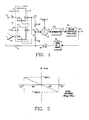
    • Figure 1 is a schematic diagram of a phase-locked loop which includes a phase detector constructed in accor­dance with one embodiment of this invention;
    • Figure 2 is a graph which illustrates the output of the phase detector of Figure 1; and
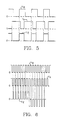
    • Figures 3, 4, 5 and 6 are a series of waveforms which illustrate the operation of the circuit of Figure 1.
  • Referring to the drawings, Figure 1 is a schemat­ic diagram of a phase-locked loop containing a phase detection circuit constructed in accordance with one embodiment of the present invention. The phase detection circuit 10 comprises a pair of bistable circuits, as represented by type D flip-flops 12 and 14, wherein each bistable circuit includes a data input D, a clock input CLK, and a reset input R. Flip-flop 12 has a NOT Q output which is electrically connected to the reset input of flip-flop 14. Flip-flop 14 has a Q output which is elec­trically connected to the reset input of flip-flop 12. The data inputs of flip-flops 12 and 14 are connected to terminals 16 and 18 respectively which receive a logic signal having a predetermined logic state that is illus­trated to be a logic 1 in this embodiment. The clock input of flip-flop 12 is connected to a terminal 20 for receiving a reference data input signal VA. An inverter 22 includes an input for receiving a second data signal VB and an output which is connected to the clock input of flip-flop 14.
  • In operation, a voltage signal VC appears at the NOT Q output of flip-flop 12 and has an average value which is proportional to the phase difference between the refer­ence data signal VA and the second data signal VB. A voltage dividing circuit branch 24 which includes the series connection of resistors 26 and 28 is connected between the NOT Q output of flip-flop 12 and the input of inverter 22. This voltage divider produces a voltage VD at the junction point 30 between the resistors that is added to a bias voltage -VDMAX/2 in summation point 32 to produce a control voltage VE. This control voltage is integrated by integrator 34 to produce a frequency control signal VF. A voltage controlled oscillator 36 responds to the frequen­cy control signal VF and produces an output voltage signal VOUT. A feedback loop comprising a divide by N circuit 38 and a buffer 40 transforms the output voltage signal VOUT into the second data signal VB.
  • Figure 2 is a plot of the average phase detection error signal VEAVG with respect to the phase difference between the input reference signal VA and the output voltage signal VOUT. The average phase error detection signal VEAVG varies linearly from a phase difference of -180° to +180°, thereby having a single zero output stable condition over the 360° control range.
  • Figure 3 is a series of waveforms which illus­trate the operation of the circuit of Figure 1 under steady state phase-locked conditions. Under these conditions, the second data signal VB and the NOT Q output of flip-flop 12 VC are seen to be 180° out-of-phase such that the phase detection error signal VE remains at zero and the output of the integrator VF is also zero. The output frequency FOUT of the voltage controlled oscillator 36 then remains constant at the VCO center frequency.
  • The waveforms of Figures 4, 5 and 6 illustrate the operation of the circuit of Figure 1 over the 360° error range. The waveforms of Figure 4 are representative of the circuit voltage signals when VA is leading VB and the duty cycle of VA is less than 50%. The waveforms of Figure 5 represent circuit operation when VB is leading VA and the duty cycle of VA is greater than 50%. Figure 6 illustrates how the phase detection error signal VE is affected as the phase difference between signals VA and VB is swept across a 360° range.
  • It should now be apparent that the phase-locked loop of Figure 1 includes a phase detector which operates independently of the duty cycle of the input reference signal VA. This circuit possesses all of the features of existing phase detectors for use in VSCF phase-locked loops and has the additional advantage of input frequency duty cycle independence. This independence is achieved by using the falling edge of the feedback signal to dictate the sign of the phase error signal. The feedback signal requires a 50% duty cycle to obtain the sign information. However, this requirement is less stringent than the need for both the input signal and the feedback signal to be precisely 50% duty cycle square waves. Generally, the output fre­quency of the VCO has a 50% duty cycle and a divide by N feedback circuit element will meet the duty cycle require­ments for all N greater than one.
  • It should be noted that the lowest "zero error" ripple produced by the circuit of Figure 1 occurs when the divide-by-N 38 output source impedance and voltage swing match the characteristics of the type D flip-flop NOT Q output. Any small voltage or resistance unbalances can be adjusted out at the summing junction 32. The same logic family with the same output characteristics would typically be used in applications of this invention. However, in the event that this is not true, a buffer 40 may be required in the feedback loop to maintain good ripple characteristics.
  • While the present invention has been described in terms of what is at present believed to be its preferred embodiment, it will be apparent to those skilled in the art that various changes and modifications may be made to the preferred embodiment without departing from the scope of the invention. It is therefore intended that the appended claims cover such changes and modifications.

Claims (6)

1. A duty cycle independent phase detecting circuit (10) comprising: a first bistable circuit (12) having a data input, a clock input, a reset input and a NOT Q output, wherein said first circuit data input is connect­ed to a predetermined logic signal and wherein said NOT Q output goes to a logic low state when a logic high signal is received at said first circuit clock input and said first circuit reset input is receiving a logic low signal, and said NOT Q output goes to a logic high state when a logic high signal is received at said first circuit reset input; and a second bistable circuit (14) having a data input, a clock input, a reset input, and a Q output, wherein said second circuit data input is connected to said predetermined logic signal and wherein said Q output goes to a logic high state when a logic high signal is received at said second circuit clock input and said second circuit reset input is receiving a logic low signal, and said Q output goes to a logic low state when a logic high signal is received at said second circuit reset input; character­ized by said NOT Q output of said first bistable circuit being connected to said reset input of said second bistable circuit; said Q output of said second bistable circuit being connected to said reset input of said first bistable circuit; means (16, 18) for connecting the data inputs of said first and second bistable circuits to a logic signal having a predetermined logic state; means (20) for connect­ing a reference data signal (VA) to the clock input of said first bistable circuit; and means (22) for connecting a second data signal (VB) to the clock input of said second bistable circuit; wherein the average value of the voltage (VC) appearing on the NOT Q output of said first bistable circuit is proportional to the phase difference between the reference data signal and the second data signal.
2. A phase detecting circuit as recited in claim 1, further characterized in that said average value varies linearly from a first predetermined voltage level to a second predetermined voltage level as the phase difference between said reference signal (VA) and said second data signal (VB) varies from -180° to +180°.
3. A phase detecting circuit as recited in claim 1, further chraacterized in that said means for connecting the second data signal to the clock input of the second bistable circuit, comprises: an inverter having an input for receiving said second data signal and having an output connected to the clock input of said second bistable circuit.
4. A phase detecting circuit as recited in claim 3, further characterized by a voltage dividing circuit branch (24) connected between the NOT Q output of said first bistable circuit and the input of said inverter.
5. A phase detecting circuit as recited in claim 4, further characterized in that said voltage dividing circuit branch comprises: a pair of resistors (26, 28) electrically connected in series, wherein the average voltage appearing at the junction of said resistors is proportional to the phase difference between said reference data signal and said second data signal.
6. A phase detecting circuit as recited in claim 1, further characterized in that said first and second bistable circuits are type D flip-flop circuits.
EP88303238A 1987-04-15 1988-04-12 Duty cycle independent phase detector Withdrawn EP0287311A3 (en)

Applications Claiming Priority (2)

Application Number Priority Date Filing Date Title
US07/038,687 US4849704A (en) 1987-04-15 1987-04-15 Duty cycle independent phase detector
US38687 1987-04-15

Publications (2)

Publication Number Publication Date
EP0287311A2 true EP0287311A2 (en) 1988-10-19
EP0287311A3 EP0287311A3 (en) 1990-03-14

Family

ID=21901335

Family Applications (1)

Application Number Title Priority Date Filing Date
EP88303238A Withdrawn EP0287311A3 (en) 1987-04-15 1988-04-12 Duty cycle independent phase detector

Country Status (4)

Country Link
US (1) US4849704A (en)
EP (1) EP0287311A3 (en)
JP (1) JPS63283232A (en)
KR (1) KR880013326A (en)

Cited By (1)

* Cited by examiner, † Cited by third party
Publication number Priority date Publication date Assignee Title
EP0519739A1 (en) * 1991-06-19 1992-12-23 Tektronix Inc. Edge integrating phase detector

Families Citing this family (13)

* Cited by examiner, † Cited by third party
Publication number Priority date Publication date Assignee Title
US5150386A (en) * 1987-05-19 1992-09-22 Crystal Semiconductor Corporation Clock multiplier/jitter attenuator
US4984255A (en) * 1989-11-15 1991-01-08 National Semiconductor Corporation Edge transition insensitive delay line system and method
US5027046A (en) * 1990-05-29 1991-06-25 Westinghouse Electric Corp. Circuit and method for monitoring voltage pulse widths
US5276661A (en) * 1990-07-18 1994-01-04 Sundstrand Corporation Master clock generator for a parallel variable speed constant frequency power system
US5264802A (en) * 1991-08-21 1993-11-23 Beg Mirza A Circuit and method for monitoring phase error modulation
GB2264597B (en) * 1992-02-29 1995-05-10 Nec Corp Frequency synthesizer and method of operation
DE4231175C1 (en) * 1992-09-17 1994-01-13 Siemens Ag Arrangement for clock recovery
US5347559A (en) * 1992-12-30 1994-09-13 Digital Equipment Corporation Apparatus and method of data transfer between systems using different clocks
CN1068473C (en) * 1994-04-07 2001-07-11 Rca.汤姆森许可公司 Phase detector for a phase-lock-loop
US5703502A (en) * 1996-05-30 1997-12-30 Sun Microsystems, Inc. Circuitry that detects a phase difference between a first, base, clock and a second, derivative, clock derived from the base clock
EP1211811A1 (en) * 2000-11-28 2002-06-05 Koninklijke Philips Electronics N.V. Fast frequency comparing circuit
CN100495921C (en) * 2006-09-01 2009-06-03 浙江天正电气股份有限公司 Intelligent digital display time relay
CN110166045B (en) * 2019-04-25 2021-06-04 复旦大学 Snapshot circuit for extracting signal change edge

Citations (3)

* Cited by examiner, † Cited by third party
Publication number Priority date Publication date Assignee Title
US3986125A (en) * 1975-10-31 1976-10-12 Sperry Univac Corporation Phase detector having a 360 linear range for periodic and aperiodic input pulse streams
DE2635892A1 (en) * 1975-08-25 1977-03-10 Hewlett Packard Co PROCEDURE AND CIRCUIT ARRANGEMENT FOR MEASURING AND DISPLAYING THE FREQUENCY RELATIONSHIP OF TWO SIGNALS
US4520319A (en) * 1982-09-30 1985-05-28 Westinghouse Electric Corp. Electronic phase detector having an output which is proportional to the phase difference between two data signals

Family Cites Families (5)

* Cited by examiner, † Cited by third party
Publication number Priority date Publication date Assignee Title
EP0054322B1 (en) * 1980-12-12 1985-07-03 Philips Electronics Uk Limited Phase sensitive detector
US4371974A (en) * 1981-02-25 1983-02-01 Rockwell International Corporation NRZ Data phase detector
US4574243A (en) * 1984-01-03 1986-03-04 Motorola, Inc. Multiple frequency digital phase locked loop
DE3576630D1 (en) * 1984-09-28 1990-04-19 Toshiba Kawasaki Kk REFERENCE SIGNAL PLAYER.
US4635280A (en) * 1985-05-28 1987-01-06 Harris Corporation Bit synchronizer for decoding data

Patent Citations (3)

* Cited by examiner, † Cited by third party
Publication number Priority date Publication date Assignee Title
DE2635892A1 (en) * 1975-08-25 1977-03-10 Hewlett Packard Co PROCEDURE AND CIRCUIT ARRANGEMENT FOR MEASURING AND DISPLAYING THE FREQUENCY RELATIONSHIP OF TWO SIGNALS
US3986125A (en) * 1975-10-31 1976-10-12 Sperry Univac Corporation Phase detector having a 360 linear range for periodic and aperiodic input pulse streams
US4520319A (en) * 1982-09-30 1985-05-28 Westinghouse Electric Corp. Electronic phase detector having an output which is proportional to the phase difference between two data signals

Cited By (1)

* Cited by examiner, † Cited by third party
Publication number Priority date Publication date Assignee Title
EP0519739A1 (en) * 1991-06-19 1992-12-23 Tektronix Inc. Edge integrating phase detector

Also Published As

Publication number Publication date
JPS63283232A (en) 1988-11-21
US4849704A (en) 1989-07-18
EP0287311A3 (en) 1990-03-14
KR880013326A (en) 1988-11-30

Similar Documents

Publication Publication Date Title
US4520319A (en) Electronic phase detector having an output which is proportional to the phase difference between two data signals
US4849704A (en) Duty cycle independent phase detector
EP0494984B1 (en) Phase detector for phase-locked loop clock recovery system
EP0304791B1 (en) Phase-locked loop having elongated time for charge and discharge
EP0671829B1 (en) Clock regeneration circuit
US6642747B1 (en) Frequency detector for a phase locked loop system
US5892380A (en) Method for shaping a pulse width and circuit therefor
US5280539A (en) Synchronous circuit for serial input signal
EP0526227A2 (en) Phase-locked loop
GB2104742A (en) Phase lock circuit
WO1987001885A1 (en) Phase comparator lock detect circuit and a synthesiser using same
EP0563945A1 (en) Phase locked loop
EP0277726A2 (en) Phase-locked loops
EP0180342A2 (en) Signal comparison circuit and phase-locked-loop using same
US4297650A (en) Phase locked loop carrier recovery circuit with false lock prevention
US4068181A (en) Digital phase comparator
US7567642B2 (en) Phase detector with extended linear operating range
EP0214676B1 (en) Clock signal regenerator arrangement
US6249188B1 (en) Error-suppressing phase comparator
US4843332A (en) Wide range digital phase/frequency detector
WO1998052284A2 (en) Phase detector arrangement
CN100417024C (en) Lock phase loop of low stable error and its correcting circuif
US4184122A (en) Digital phase comparison apparatus
GB2161660A (en) Digital phase/frequency detector having output latch
US4884035A (en) Wide range digital phase/frequency detector

Legal Events

Date Code Title Description
PUAI Public reference made under article 153(3) epc to a published international application that has entered the european phase

Free format text: ORIGINAL CODE: 0009012

AK Designated contracting states

Kind code of ref document: A2

Designated state(s): DE FR GB

PUAL Search report despatched

Free format text: ORIGINAL CODE: 0009013

AK Designated contracting states

Kind code of ref document: A3

Designated state(s): DE FR GB

17P Request for examination filed

Effective date: 19900907

RAP1 Party data changed (applicant data changed or rights of an application transferred)

Owner name: SUNDSTRAND CORPORATION

17Q First examination report despatched

Effective date: 19921005

STAA Information on the status of an ep patent application or granted ep patent

Free format text: STATUS: THE APPLICATION HAS BEEN WITHDRAWN

18W Application withdrawn

Withdrawal date: 19940816