EP0303343A1 - Addressing liquid crystal cells - Google Patents
Addressing liquid crystal cells Download PDFInfo
- Publication number
- EP0303343A1 EP0303343A1 EP88305826A EP88305826A EP0303343A1 EP 0303343 A1 EP0303343 A1 EP 0303343A1 EP 88305826 A EP88305826 A EP 88305826A EP 88305826 A EP88305826 A EP 88305826A EP 0303343 A1 EP0303343 A1 EP 0303343A1
- Authority
- EP
- European Patent Office
- Prior art keywords
- waveform
- data
- pulses
- liquid crystal
- pixels
- Prior art date
- Legal status (The legal status is an assumption and is not a legal conclusion. Google has not performed a legal analysis and makes no representation as to the accuracy of the status listed.)
- Granted
Links
Images

Classifications
-
- G—PHYSICS
- G02—OPTICS
- G02F—OPTICAL DEVICES OR ARRANGEMENTS FOR THE CONTROL OF LIGHT BY MODIFICATION OF THE OPTICAL PROPERTIES OF THE MEDIA OF THE ELEMENTS INVOLVED THEREIN; NON-LINEAR OPTICS; FREQUENCY-CHANGING OF LIGHT; OPTICAL LOGIC ELEMENTS; OPTICAL ANALOGUE/DIGITAL CONVERTERS
- G02F1/00—Devices or arrangements for the control of the intensity, colour, phase, polarisation or direction of light arriving from an independent light source, e.g. switching, gating or modulating; Non-linear optics
- G02F1/01—Devices or arrangements for the control of the intensity, colour, phase, polarisation or direction of light arriving from an independent light source, e.g. switching, gating or modulating; Non-linear optics for the control of the intensity, phase, polarisation or colour
- G02F1/13—Devices or arrangements for the control of the intensity, colour, phase, polarisation or direction of light arriving from an independent light source, e.g. switching, gating or modulating; Non-linear optics for the control of the intensity, phase, polarisation or colour based on liquid crystals, e.g. single liquid crystal display cells
- G02F1/133—Constructional arrangements; Operation of liquid crystal cells; Circuit arrangements
-
- G—PHYSICS
- G09—EDUCATION; CRYPTOGRAPHY; DISPLAY; ADVERTISING; SEALS
- G09G—ARRANGEMENTS OR CIRCUITS FOR CONTROL OF INDICATING DEVICES USING STATIC MEANS TO PRESENT VARIABLE INFORMATION
- G09G3/00—Control arrangements or circuits, of interest only in connection with visual indicators other than cathode-ray tubes
- G09G3/20—Control arrangements or circuits, of interest only in connection with visual indicators other than cathode-ray tubes for presentation of an assembly of a number of characters, e.g. a page, by composing the assembly by combination of individual elements arranged in a matrix no fixed position being assigned to or needed to be assigned to the individual characters or partial characters
- G09G3/34—Control arrangements or circuits, of interest only in connection with visual indicators other than cathode-ray tubes for presentation of an assembly of a number of characters, e.g. a page, by composing the assembly by combination of individual elements arranged in a matrix no fixed position being assigned to or needed to be assigned to the individual characters or partial characters by control of light from an independent source
- G09G3/36—Control arrangements or circuits, of interest only in connection with visual indicators other than cathode-ray tubes for presentation of an assembly of a number of characters, e.g. a page, by composing the assembly by combination of individual elements arranged in a matrix no fixed position being assigned to or needed to be assigned to the individual characters or partial characters by control of light from an independent source using liquid crystals
- G09G3/3611—Control of matrices with row and column drivers
-
- G—PHYSICS
- G02—OPTICS
- G02F—OPTICAL DEVICES OR ARRANGEMENTS FOR THE CONTROL OF LIGHT BY MODIFICATION OF THE OPTICAL PROPERTIES OF THE MEDIA OF THE ELEMENTS INVOLVED THEREIN; NON-LINEAR OPTICS; FREQUENCY-CHANGING OF LIGHT; OPTICAL LOGIC ELEMENTS; OPTICAL ANALOGUE/DIGITAL CONVERTERS
- G02F1/00—Devices or arrangements for the control of the intensity, colour, phase, polarisation or direction of light arriving from an independent light source, e.g. switching, gating or modulating; Non-linear optics
- G02F1/01—Devices or arrangements for the control of the intensity, colour, phase, polarisation or direction of light arriving from an independent light source, e.g. switching, gating or modulating; Non-linear optics for the control of the intensity, phase, polarisation or colour
- G02F1/13—Devices or arrangements for the control of the intensity, colour, phase, polarisation or direction of light arriving from an independent light source, e.g. switching, gating or modulating; Non-linear optics for the control of the intensity, phase, polarisation or colour based on liquid crystals, e.g. single liquid crystal display cells
- G02F1/133—Constructional arrangements; Operation of liquid crystal cells; Circuit arrangements
- G02F1/1333—Constructional arrangements; Manufacturing methods
- G02F1/133382—Heating or cooling of liquid crystal cells other than for activation, e.g. circuits or arrangements for temperature control, stabilisation or uniform distribution over the cell
-
- G—PHYSICS
- G09—EDUCATION; CRYPTOGRAPHY; DISPLAY; ADVERTISING; SEALS
- G09G—ARRANGEMENTS OR CIRCUITS FOR CONTROL OF INDICATING DEVICES USING STATIC MEANS TO PRESENT VARIABLE INFORMATION
- G09G2320/00—Control of display operating conditions
- G09G2320/04—Maintaining the quality of display appearance
- G09G2320/041—Temperature compensation
Abstract
Description
- This invention relates to the addressing on a co-ordinate basis of ferroelectric liquid crystal cells exhibiting negative dielectric anisotropy.
- Published United Kingdom Patent Specification No. 2173629A describes one such addressing method which involves applying bipolar data pulses in parallel to one set of electrodes while unipolar strobe pulses are applied serially to the other set so as to write the data into the cell on a line-by-line basis. The unipolar nature of the strobe pulses dictates that a single strobe pulse can be used for switching pixels in one direction only. One way of overcoming the difficulty that this presents is to use the strobe and data pulses to set selected pixels of a group into one state (one data significance) having first used a blanking pulse of opposite polarity to the strobe pulse to set all the pixels of that group into the other state (the other data significance). The group of pixels may for instance comprise a single line of pixels, a limited set of lines, or the set of all lines of the display. An alternative way of overcoming this difficulty, the way employed in
GB 2 173 629A, is to arrange for the polarity of the strobe pulses to be regularly alternated. Under these circumstances selected pixels of a line can be set into the one state with the aid of a strobe pulse while those pixels of that line required to be set into the other state have to wait to be set into their required state until theadvent of a strobe pulse of the opposite polarity. - For any particular chemical composition of the liquid crystal layer it is found that there is, at any given temperature of operation within the working range, a particular voltage threshold for achieving switching with pulses of a particular duration. The magnitude of the strobe pulses is +VS or -VS, and that the data pulses make excursions between +VD and -VD, the switching theshold VTH is given by VTH = |VS+VD|. The value of VD affects what happens to the unselected pixels, and so there is an optimum partioning of VTH between VS and VD in order to achieve maximum contrast. The optimum value of the ratio VS : VD is generally found to be temperature dependent.
- One way of avoiding problems associated with temperature dependent switching effects is to operate the device with a thermostatted liquid crystal layer, but this option may be inappropriate, or difficult or impossible to implement in certain situations. An alternative option is to allow the temperature to vary, at least within a restricted range, and to arrange to compensate such changes as do occur by making appropriate changes to the durations of the strobe and data pulse waveforms while maintaining their amplitudes unchanged. Particular circumstances can make this approach inconvenient or otherwise difficult to implement. A further alternative is to compensate for temperature changes by adjusting the strobe and data pulse waveform amplitudes rather than their durations. This is the option with which the present invention is particularly concerned. However, when using this approach with ferroelectric liquid crystal layers exhibiting negative dielectric anisotropy, we have found that the range of satisfactory operating temperature has a relatively sharp cut-off at the upper end, above which there is a marked deterioriation in contrast. The present invention is particularly concerned with extending the useful range of operating temperature.
- According to the present invention there is provided a method of coordinate addressing a liquid crystal cell, which method involves applying unipolar strobe pulses to a first set of electrodes which, together with a second set of electrodes define the pixels of the cell, and applying bipolar pulses to a second set of electrodes, characterised in that at least above a given temperature, an alternating voltage stabilisation waveform is applied to the pixels which stabilisation waveform is at a higher frequency than the fundamental frequency that is defined by the waveform of one of said bipolar pulses.
- According to a preferred aspect of the present invention there is provided a method of addressing a matrix-array type liquid crystal cell with a ferroelectric liquid crystal layer exhibiting negative dielectric anisotropy whose pixels are defined by the areas of overlap between the members of a first set of electrodes on one side of the liquid crystal layer and the members of a second set on the other side of the layer, in which method the pixels are selectively addressed on a line-by-line basis by the application of unipolar strobing pulses serially to the members of the first set of electrodes while charge balanced bipolar data pulses are applied in parallel to the members of the second set, the positive going parts of the bipolar data pulses being synchronised with a strobe pulse for one data significance and the negative going parts being synchronised with the strobe pulse for the other data significance, wherein the amplitudes of the waveforms of the strobing and data pulses are changed in response to changes in the temperature of the liquid crystal layer, and characterised in that at least above a given temperature an alternating voltage stabilisation waveform is applied to the pixels between consecutive strobings, which stabilisation waveform is at a frequency which is an even multiple of the fundamental frequency that is defined by the bipolar data pulse waveform.
- The invention also resides in a liquid crystal device including a liquid crystal cell with a ferroelectric liquid crystal layer exhibiting negative dielectric anisotropy whose pixels are defined by areas of overlap between the members of a first set of electrodes on one side of the liquid crystal layer and the members of a second set on the other side of the layer, which device includes strobing means and data entry drive means adapted to address the pixels selectively on a line-by-line basis by the application of unipolar strobing pulses serially to the members of the first set of electrodes while charge balanced bipolar data pulses are applied in parallel to the members of the second set, the positive going parts of the bipolar pulses being synchronised with the strobe pulse for one data significance and the negative going parts being synchronised with the strobe pulse for the other data significance, characterised in that the device also includes a waveform generator, a temperature sensor, and a waveform voltage amplitude controller, wherein the temperature sensor is adapted to sense the temperature of the cell and the waveform controller is adapted, in response to an input from the temperature sensor, to control the voltage amplitudes of the strobe and data pulse waveforms, and of a stabilisation waveform applied to the pixels between consecutive strobings, the fundamental frequency of which stabilisation waveform is an even multiple of the fundamental frequency that is defined by the bipolar data pulse waveform.
- The use of the alternating voltage stabilisation waveform is only required above a certain critical threshold temperature. Beneath this temperature it is surmised that the magnitude of the data pulse waveform is enough to provide the requisite stabilisation. It is therefore not necessary to continue with the stabilisation waveform below the critical threshold temperature, though it may be maintained, making any necessary adjustment to the magnitudes of the strobe and data pulse waveforms.
- In principle the stabilisation waveform can be applied to either set of electrodes, or even be shared between them, but generally it is preferred to apply it to the set of electrodes to which the strobe pulse waveform is applied. The stabilisation waveform can be applied on a continuous basis, but since its intended effect is to stabilise (hold) the individual pixels in their pre-existing states, whereas the strobe pulse isintended to enable selected pixels to be switched to their other states, it is generally preferred to remove the application of the stabilisation waveform from any particular electrode while it is in receipt of any strobe pulse. There can also be advantage in removing the stabilisation waveform, not only at the moment of the application of the strobe pulse, but also a short time before its application in order to allow the stabilisation effect of the waveform to decay before the onset of the strobe pulse.
- The appropriate magnitude of the stabilisation waveform above the threshold temperature may itself be temperature dependent. Generally, it may be found convenient to use a frequency that is a low-order even multiple of the fundamental frequency of the data pulse waveform, typically twice. In these circumstances the range of satisfactory operating temperature of the device may be curtailed at its upper end by the optical response of the liquid crystal becoming fast enough to enable it to track, to a significant extent, the alternating field of the stabilisation waveform. Under these circumstances it may be possible to extend the useful operating temperature range by switching the stabilisation waveform to a higher frequency once this condition begins to become manifest, changing for instance from a frequency that is twice the fundamental frequency to one that is four times that frequency.
- There follows a description of the operation of a matrix array type smectic liquid crystal cell embodying the invention in a preferred form. The description refers to the accompanying drawings in which:-
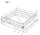
- Figure 1 depicts a schematic perspective view of a ferroelectric liquid crystal cell,
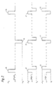
- Figure 2 depicts waveforms used to address the cell of Figure 1,
- Figure 3 depicts the relation voltage and temperature of the waveforms of Figure 2, and
- Figure 4 depicts the basic elements of the drive circuitry employed to drive the cell of Figure 1.
- Referring now to Figure 1, a hermetically sealed envelope for a liquid crystal layer is formed by securing together two
glass sheets perimeter seal 13. The inward facing surfaces of the two sheets carrytransparent electrode layers electrode layers layer 14 extend transversely of those oflayer 15 so as to define a pixel at each elemental area where an electrode strip oflayer 15 is overlapped by a strip oflayer 14. The thickness of the liquid crystal layer contained within the resulting envelope is determined by a light scattering of polymeric spheres of uniform diameter throughout the area of the cell. Conveniently the cell is filled by applying a vacuum to an aperture (not shown) through one of the glass sheets in one corner of the area enclosed by the perimeter seal so as to causethe liquid crystal medium to enter the cell by way of another aperture (not shown) located in the diagonally opposite corner. (Subsequent to the filling operation the two apertures are sealed.) The filling operation is carried out with the filling material heated into its nematic or isotropic phase so as to reduce its viscosity to a suitably low value. It will be noted that the basic construction of the cell is similar to that of for instance a conventional twisted nematic, except of course for the parallel alignment of the rubbing directions. - Typically the thickness of the
perimeter seal 13, and hence of the liquid crystal layer, is between 1.5 and 3 um, but thinner or thicker layer thicknesses may be required to suit particular applications. A preferred thickness is 2um. A suitable material for the filling is the smectic C eutectic marketed by BDH of Poole in Dorset under the designation of SCE 3. This material, which exhibits negative dielectric anistropy at least over the frequency range from 1kHz to 40kHz, passes through the smectic A phase on cooling into the smectic C phase from the isotropic phase. In the case of a 2um thick liquid crystal layer confined between the rubbed surfaces the entry of the material into the smectic A phase causes the smectic layers to be formed with bookshelf alignment (layers extending in planes to which the rubbing direction is normal), and this alignment of the smectic layers is found to be preserved when the material makes the transition into the smectic C phase. - Referring to Figure 2, a preferred way of addressing the cell in a matrix basis employs charge balanced
bipolar data pulses unipolar strobe pulses Data pulse 21, arbitrarily designated a data 'O' pulse, comprises a voltage excursion to +VD for a duration ts followed immediately by a voltage excursion to -VD for a further duration ts.Data pulse 22, arbitrarily designated a data 'l' pulse, is similar todata pulse 21, but the order of the voltage excursions is reversed.Strobe pulse 23 comprises a voltage excursion to +VS for a duration ts whilestrobe pulse 24 comprises a voltage excursion to -VS, also of duration tS. - The pixels of the display are defined by the areas of overlap between the members of one set of electrode strips and those of the other. The unipolar strobe pulses are synchronised with the first halves of the data pulses. Therefore when a pixel is simultaneously addressed with a positive-going
strobe pulse 23 and a data 'O'pulse 21 it experiences a potential difference of (VS-VD) for ts, followed by a potential difference of +VD. A pixel addressed with astrobe pulse 23 and a data '1'pulse 22 experiences a potential difference of (VS+VD) for ts, followed by a potential difference of -VD. Correspondingly, a pixel addressed simultaneously with a negative-goingstrobe pulse 24 and a data 'O'pulse 21, experiences a potential difference of -(VS+VD) for ts, followed by a potential difference of +VD. Finally, a pixel addressed with a negative-goingstrobe pulse 24 and a data 'l'pulse 22 experiences a potential difference of -(VS-VD) for ts, followed by a potential difference of -VD. - The values of VS and VD are chosen so that a potential difference of +(VS+VD) is sufficient to switch a pixel into its 'l' state while a potential difference of -(VS+VD) is sufficient to switch it into its '0' state. This switching must be effective with a switching stimulus of duration ts notwithstanding that it may be immediately preceded with an oppositively directed stimulus of magnitude VD, and that it will be immediately followed by an oppositely directed stimulus of magnitude VD. Additionally, the values of VS and VD must be chosen so that the other stimuli to which a pixel is liable to be exposed do not produce switching. For instance, while other lines are being addressed, a pixel is subjected to a stimulus of magnitude VD for a duration 2ts whenever a bipolar data pulse of one data significance is immediately followed by a data pulse of the other data significance. This must not produce switching. Similarly switching must not be produced by a stimulus comprising +VD for ts immediately followed by +(VS-VD) for ts, itself immediately followed by +VD for a further ts. This stimulus is produced by the data sequence 'l'-'O' when a positive going
strobe pulse 23 is coincident with the data 'O'. Some relaxation of these conditions may be possible by providing intervals between consecutive data pulses, and/or by providing an interval between the two excursions of each bipolar data pulse, and/or by using an asymmetric form of charge balanced bipolar data pulse in which one excursion is m times the amplitude of the other, but only 1/mth its duration. - The positive-going
strobe pulse 23 will co-operate with a data 'l' pulse to produced a stimulus of magnitude VS+VD, and thus is capable of being used to set selected pixels from a 'O' state into a 'l' state. It is not capable however of being used to set pixels from a 'l' state into a 'O' state because with neither significance of data pulse will it produce a stimulus of -(VS+VD). Conversely a negative-goingstrobe pulse 24 can set 'l' state pixels into the 'O' state but not 'O' state pixels into the 'l' state. For this reason the addressing is generally operated with the polarity of the strobe pulse being reversed with each refreshing of the cell. It should be appreciated however that if for some reason it is desired to provide a slightly longer interval between polarity reversals (occupying a small number of refreshings), this can be accommodated, though it will be evident that this will entail the possibility of certain pixels being retained in their wrong states for correspondingly longer periods before being set into their correct states. - In the foregoing discussion it has been assumed that the strobe pulse is synchronised with the first voltage excursion of the bipolar data pulses. It should be appreciated that a satisfactory alternative involves synchronisation of the strobe pulses with the second voltage excursions of the data pulses. In this case the data significance of the data pulses is reversed.
- According to one theory of the behaviour of smectic C filled ferroelectric cells with bookshelf alignment of their smectic layers, the molecules should be capable of being switched by single pulses between two stable states in one of which the average direction of the molecular axes lies in the plane of the liquid crystal layer at + to the smectic layer normal, and in the other of which the corresponding angle is -. In practice however, it is found that the initial response to a single switching pulse relaxes substantially once that pulse has terminated. This relaxation is a great impediment to any form of multiplexing, but it is found that it can be avoided by the superimposing of an alternating potential at a frequency for which the liquid crystal exhibits negative dielectric anisotropy. Such an alternating potential is found to be capable of stabilising the switching of the cell substantially into its two fully switched states.
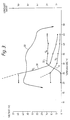
- When the addressing of the pixels of the cell of Figure 1 is achieved using the addressing scheme of Figure 2 the data stream is found, under appropriate conditions to provide a sufficient alternating voltage stimulus to the pixels between consecutive refreshings to prevent any appreciable relaxation effects without having to have recourse to any separate signal for stabilisation purposes. However, with increasing temperature, the efficacy of the data stream in providing this stabilisation is progressively reduced until the point is reached where separate stabilisation at a frequency greater than the fundamental frequency of the data stream does become necessary. In the particular example of a cell filled with a 2um thick layer of SCE 3 driven with the addressing scheme of Figure 2 at 1/6th video line rate (line address time 384 us, ts=192us) the stabilisation provided by the data stream begins to fail at a temperature of between 25° and 30°C, with the result that at the upper end of this range the contrast of the display has fallen away so much as to render it effectively useless. Figure 3 depicts the effect of superimposing an alternating voltage for stabilisation (holding) purposes. In this instance the stabilisation (holding) voltage VH is a square wave with a fundamental frequency of twice that of the data pulses. This is applied in parallel to the electrodes to which the strobe pulses are serially applied, being removed from each of those electrodes in turn while it is addressed with a strobe pulse. It was found convenient for this removal of the stabilisation to be for the 192us of the strobe pulse itself, and, so as to make it equal to one line address period, for the 192us immediately following the strobe pulse. In Figure 3 the magnitude of the optimum strobe voltage VS expressed as a function of temperature is given by
curve 30, that of the optimum data voltage VD is given bycurve 31, while that of the applied stabilisation (holding) voltage VH is given bycurve 32. From these curves it is seen that the magnitude of stabilisation voltage, VH, rises from zero to a maximum over thetemperature range 25° to 30°C, which is also atemperature range over which the values of optimum strobe and data voltages are rapidly changing. The portions ofcurves curve 33 which is a plot, expressed as a function of temperature, of the resulting contrast ratio of the display. Below about 20°C the contrast ratio is falling off rapidly because of the slow response of the liquid crystal, whereas above 45°C the contrast ratio is falling off rapidly because the response is fast enough for the cell to be beginning to be switched to an appreciable extent by the stabilisation signal. This upper limit of the useful temperature range can be extended to higher temperatures by changing over to a higher frequency for the stabilisation voltage. - Figure 4 depicts the basic elements of circuitry employed to drive the cell. The display cell itself is depicted at 40, and is addressed by means of sets of row and
column drivers line 43 to adata receiver unit 44 which transmits data signals online 45 to the set ofcolumn drivers 42. The data receiver unit also transmits a part of thereceived signal to atiming control unit 46 which employs this to produce a signal of appropriate frequency and phase for application to the set ofrow drivers 41 online 47 for controlling the synchronisation of the strobe. The timing control unit also uses the incoming signal to produce a phase locked signal at the stabilisation signal frequency which is applied to the set of row drivers online 48 for controlling the synchronisation of the stabilisation signals applied to the cell via the row drivers. - The signals applied to the drivers over
lines voltage control unit 50 receiving power from a stabilisedpower supply 51. Atemperature sensor 52 attached to thecell 40 connected with atemperature measuring circuit 53 provides a temperature indicating input to thevoltage control unit 50 which contains in ROM storage look-up tables of the required voltage/temperature relationships in respect of the data, strobe and stabilisation voltages. The data pulse and voltages and voltage reference ± VD and O are supplied to the column drivers online 54, while the strobe pulse, stabilisation voltage and voltage reference voltages ± VS, ± VH and O are supplied to the row drivers online 55.
Claims (8)
Priority Applications (1)
| Application Number | Priority Date | Filing Date | Title |
|---|---|---|---|
| AT88305826T ATE83577T1 (en) | 1987-07-18 | 1988-06-27 | ADDRESSING OF LIQUID CRYSTAL CELLS. |
Applications Claiming Priority (3)
| Application Number | Priority Date | Filing Date | Title |
|---|---|---|---|
| GB8716992 | 1987-07-18 | ||
| GB8716992A GB2207272B (en) | 1987-07-18 | 1987-07-18 | Addressing liquid crystal cells |
| CA000603901A CA1333506C (en) | 1987-07-18 | 1989-06-26 | Addressing liquid crystal cells |
Publications (2)
| Publication Number | Publication Date |
|---|---|
| EP0303343A1 true EP0303343A1 (en) | 1989-02-15 |
| EP0303343B1 EP0303343B1 (en) | 1992-12-16 |
Family
ID=25672838
Family Applications (1)
| Application Number | Title | Priority Date | Filing Date |
|---|---|---|---|
| EP88305826A Expired - Lifetime EP0303343B1 (en) | 1987-07-18 | 1988-06-27 | Addressing liquid crystal cells |
Country Status (8)
| Country | Link |
|---|---|
| US (1) | US4917469A (en) |
| EP (1) | EP0303343B1 (en) |
| JP (1) | JP2633312B2 (en) |
| KR (1) | KR0136798B1 (en) |
| AT (1) | ATE83577T1 (en) |
| CA (1) | CA1333506C (en) |
| DE (1) | DE3876713T2 (en) |
| GB (1) | GB2207272B (en) |
Cited By (5)
| Publication number | Priority date | Publication date | Assignee | Title |
|---|---|---|---|---|
| EP0438093A2 (en) * | 1990-01-16 | 1991-07-24 | Honeywell Inc. | Apparatus and method for temperature compensation of liquid crystal displays |
| EP0450640A2 (en) * | 1990-04-06 | 1991-10-09 | Canon Kabushiki Kaisha | Display apparatus |
| FR2673027A1 (en) * | 1991-02-20 | 1992-08-21 | Asahi Optical Co Ltd | Liquid crystal display device |
| WO1995024715A1 (en) * | 1994-03-07 | 1995-09-14 | The Secretary Of State For Defence In Her Britannic Majesty's Government Of The United Kingdom Of Great Britain And Northern Ireland | Temperature compensation of ferroelectric liquid crystal displays |
| GB2301450A (en) * | 1994-03-07 | 1996-12-04 | Secr Defence | Temperature compensation of ferroelectric liquid crystal displays |
Families Citing this family (32)
| Publication number | Priority date | Publication date | Assignee | Title |
|---|---|---|---|---|
| GB8726996D0 (en) * | 1987-11-18 | 1987-12-23 | Secr Defence | Multiplex addressing of ferro-electric liquid crystal displays |
| US5117224A (en) * | 1988-02-16 | 1992-05-26 | Casio Computer, Ltd. | Color liquid crystal display apparatus |
| GB8808812D0 (en) * | 1988-04-14 | 1988-05-18 | Emi Plc Thorn | Display device |
| US5029982A (en) * | 1989-09-11 | 1991-07-09 | Tandy Corporation | LCD contrast adjustment system |
| US5132825A (en) * | 1989-10-18 | 1992-07-21 | Asahi Kogaku Kogyo Kabushiki Kaisha | Image processing apparatus having control means for adjusting the color temperature of the displayed image |
| US5196955A (en) * | 1990-05-24 | 1993-03-23 | Semiconductor Energy Laboratory Co., Ltd. | Ferroelectric liquid crystal optical device with viscosity not more than 30000 cps |
| IT1240381B (en) * | 1990-07-06 | 1993-12-10 | Seleco Spa | PILOTING SIGNAL CIRCUIT FOR DISPLAY |
| US5798814A (en) * | 1990-08-28 | 1998-08-25 | Semiconductor Energy Laboratory Co., Ltd. | Method of driving a ferroelectric liquid crystal optical device |
| JP2990297B2 (en) * | 1990-09-10 | 1999-12-13 | セイコーインスツルメンツ株式会社 | Liquid crystal light valve device and liquid crystal light valve driving method |
| NL9002516A (en) * | 1990-11-19 | 1992-06-16 | Philips Nv | DISPLAY DEVICE AND METHOD OF MANUFACTURE THEREOF. |
| US6320568B1 (en) * | 1990-12-31 | 2001-11-20 | Kopin Corporation | Control system for display panels |
| DE69319943T2 (en) * | 1992-02-28 | 1999-02-11 | Canon Kk | Liquid crystal display device |
| DE4221784A1 (en) * | 1992-07-03 | 1994-01-05 | Hoechst Ag | Electrical addressing of ferroelectric liquid crystal displays |
| US6115021A (en) * | 1994-07-04 | 2000-09-05 | Sharp Kabushiki Kaisha | Method and apparatus for driving a liquid crystal panel using a ferroelectric liquid crystal material having a negative dielectric anisotropy |
| GB2293906A (en) * | 1994-10-03 | 1996-04-10 | Sharp Kk | Liquid crystal display |
| JPH0980388A (en) * | 1995-09-11 | 1997-03-28 | Denso Corp | Matrix type liquid crystal display device |
| KR100506958B1 (en) * | 1995-12-15 | 2005-10-27 | 코닌클리케 필립스 일렉트로닉스 엔.브이. | LCD display device |
| GB2313224A (en) | 1996-05-17 | 1997-11-19 | Sharp Kk | Ferroelectric liquid crystal device |
| JPH1039772A (en) * | 1996-07-29 | 1998-02-13 | Mitsubishi Electric Corp | Projection type liquid crystal display device |
| US6545654B2 (en) | 1996-10-31 | 2003-04-08 | Kopin Corporation | Microdisplay for portable communication systems |
| US6909419B2 (en) * | 1997-10-31 | 2005-06-21 | Kopin Corporation | Portable microdisplay system |
| US6552704B2 (en) | 1997-10-31 | 2003-04-22 | Kopin Corporation | Color display with thin gap liquid crystal |
| US6476784B2 (en) | 1997-10-31 | 2002-11-05 | Kopin Corporation | Portable display system with memory card reader |
| JP2000132145A (en) * | 1998-10-28 | 2000-05-12 | Alps Electric Co Ltd | Image display device |
| US6999057B2 (en) * | 2000-02-22 | 2006-02-14 | Kopin Corporation | Timing of fields of video |
| KR100523591B1 (en) * | 2002-04-09 | 2005-10-26 | 이근홍 | Electrode and its manufacturing method using rare earth element |
| KR20030095013A (en) * | 2002-06-11 | 2003-12-18 | 이수테크 주식회사 | Ionic water electrode and method for manufacturing the same |
| KR20030095012A (en) * | 2002-06-11 | 2003-12-18 | 이수테크 주식회사 | Ionic water electrode and method for manufacturing the same |
| JP5105694B2 (en) * | 2003-12-24 | 2012-12-26 | 株式会社半導体エネルギー研究所 | Display device and electronic device |
| KR100627387B1 (en) * | 2004-06-29 | 2006-09-21 | 삼성에스디아이 주식회사 | A liquid crystal display and a driving method thereof |
| KR100599756B1 (en) * | 2004-06-29 | 2006-07-12 | 삼성에스디아이 주식회사 | A liquid crystal display and a driving method thereof |
| KR102305334B1 (en) * | 2019-10-04 | 2021-09-28 | 주식회사 웨스코일렉트로드 | A method for manufacturing anode plate |
Citations (6)
| Publication number | Priority date | Publication date | Assignee | Title |
|---|---|---|---|---|
| DE2316863B2 (en) * | 1972-04-06 | 1977-02-24 | Matsushita Electric Industrial Co., Ltd., Kadoma, Osaka (Japan) | PROCEDURE FOR OPERATING A LIQUID CRYSTAL DISPLAY DEVICE |
| US4100540A (en) * | 1975-11-18 | 1978-07-11 | Citizen Watch Co., Ltd. | Method of driving liquid crystal matrix display device to obtain maximum contrast and reduce power consumption |
| US4242679A (en) * | 1977-09-13 | 1980-12-30 | Kabushiki Kaisha Suwa Seikosha | Liquid crystal display mechanism |
| FR2546324A1 (en) * | 1983-05-17 | 1984-11-23 | Thomson Csf | Visual display device with memory held on |
| GB2173629A (en) * | 1986-04-01 | 1986-10-15 | Stc Plc | Addressing liquid crystal cells |
| FR2581209A1 (en) * | 1985-04-26 | 1986-10-31 | Canon Kk | Liquid-crystal optical device |
Family Cites Families (6)
| Publication number | Priority date | Publication date | Assignee | Title |
|---|---|---|---|---|
| US4045791A (en) * | 1972-04-06 | 1977-08-30 | Matsushita Electric Industrial Co., Ltd. | Apparatus for driving liquid crystal display device wherein the signal applied thereto is varied in accordance with the temperature of the device |
| JPS58186796A (en) * | 1982-04-26 | 1983-10-31 | 社団法人日本電子工業振興協会 | Liquid crystal display unit and driving thereof |
| FR2541807B1 (en) * | 1983-02-24 | 1985-06-07 | Commissariat Energie Atomique | METHOD OF SEQUENTIAL CONTROL OF A MATRIX IMAGER USING THE CHOLESTERIC-NEMATIC PHASE TRANSITION EFFECT OF A LIQUID CRYSTAL |
| GB2173337B (en) * | 1985-04-03 | 1989-01-11 | Stc Plc | Addressing liquid crystal cells |
| GB2173336B (en) * | 1985-04-03 | 1988-04-27 | Stc Plc | Addressing liquid crystal cells |
| JPS61249024A (en) * | 1985-04-26 | 1986-11-06 | Canon Inc | Liquid crystal optical element |
-
1987
- 1987-07-18 GB GB8716992A patent/GB2207272B/en not_active Expired - Lifetime
-
1988
- 1988-06-27 AT AT88305826T patent/ATE83577T1/en not_active IP Right Cessation
- 1988-06-27 EP EP88305826A patent/EP0303343B1/en not_active Expired - Lifetime
- 1988-06-27 DE DE8888305826T patent/DE3876713T2/en not_active Expired - Fee Related
- 1988-07-01 US US07/214,532 patent/US4917469A/en not_active Expired - Lifetime
- 1988-07-14 JP JP63176186A patent/JP2633312B2/en not_active Expired - Fee Related
- 1988-07-18 KR KR1019880009006A patent/KR0136798B1/en not_active IP Right Cessation
-
1989
- 1989-06-26 CA CA000603901A patent/CA1333506C/en not_active Expired - Fee Related
Patent Citations (6)
| Publication number | Priority date | Publication date | Assignee | Title |
|---|---|---|---|---|
| DE2316863B2 (en) * | 1972-04-06 | 1977-02-24 | Matsushita Electric Industrial Co., Ltd., Kadoma, Osaka (Japan) | PROCEDURE FOR OPERATING A LIQUID CRYSTAL DISPLAY DEVICE |
| US4100540A (en) * | 1975-11-18 | 1978-07-11 | Citizen Watch Co., Ltd. | Method of driving liquid crystal matrix display device to obtain maximum contrast and reduce power consumption |
| US4242679A (en) * | 1977-09-13 | 1980-12-30 | Kabushiki Kaisha Suwa Seikosha | Liquid crystal display mechanism |
| FR2546324A1 (en) * | 1983-05-17 | 1984-11-23 | Thomson Csf | Visual display device with memory held on |
| FR2581209A1 (en) * | 1985-04-26 | 1986-10-31 | Canon Kk | Liquid-crystal optical device |
| GB2173629A (en) * | 1986-04-01 | 1986-10-15 | Stc Plc | Addressing liquid crystal cells |
Cited By (10)
| Publication number | Priority date | Publication date | Assignee | Title |
|---|---|---|---|---|
| EP0438093A2 (en) * | 1990-01-16 | 1991-07-24 | Honeywell Inc. | Apparatus and method for temperature compensation of liquid crystal displays |
| EP0438093A3 (en) * | 1990-01-16 | 1992-02-05 | Honeywell Inc. | Apparatus and method for temperature compensation of liquid crystal displays |
| EP0450640A2 (en) * | 1990-04-06 | 1991-10-09 | Canon Kabushiki Kaisha | Display apparatus |
| EP0450640A3 (en) * | 1990-04-06 | 1992-11-19 | Canon Kabushiki Kaisha | Display apparatus |
| US5754153A (en) * | 1990-04-06 | 1998-05-19 | Canon Kabushiki Kaisha | Display apparatus |
| FR2673027A1 (en) * | 1991-02-20 | 1992-08-21 | Asahi Optical Co Ltd | Liquid crystal display device |
| WO1995024715A1 (en) * | 1994-03-07 | 1995-09-14 | The Secretary Of State For Defence In Her Britannic Majesty's Government Of The United Kingdom Of Great Britain And Northern Ireland | Temperature compensation of ferroelectric liquid crystal displays |
| GB2301450A (en) * | 1994-03-07 | 1996-12-04 | Secr Defence | Temperature compensation of ferroelectric liquid crystal displays |
| GB2301450B (en) * | 1994-03-07 | 1998-01-14 | Secr Defence | Temperature compensation of ferro-electric liquid crystal displays |
| US5825344A (en) * | 1994-03-07 | 1998-10-20 | The Secretary Of State For Defence In Her Britannic Majesty's Government Of The United Kingdom Of Great Britain And Northern Ireland | Temperature compensation of ferro-electric liquid crystal displays |
Also Published As
| Publication number | Publication date |
|---|---|
| JP2633312B2 (en) | 1997-07-23 |
| CA1333506C (en) | 1994-12-13 |
| DE3876713D1 (en) | 1993-01-28 |
| US4917469A (en) | 1990-04-17 |
| GB2207272A (en) | 1989-01-25 |
| GB8716992D0 (en) | 1987-08-26 |
| GB2207272B (en) | 1991-08-14 |
| EP0303343B1 (en) | 1992-12-16 |
| KR890002701A (en) | 1989-04-11 |
| KR0136798B1 (en) | 1998-04-28 |
| DE3876713T2 (en) | 1993-04-22 |
| JPS6437536A (en) | 1989-02-08 |
| ATE83577T1 (en) | 1993-01-15 |
Similar Documents
| Publication | Publication Date | Title |
|---|---|---|
| EP0303343B1 (en) | Addressing liquid crystal cells | |
| EP0240222B1 (en) | Addressing liquid crystal cells | |
| EP0197742B1 (en) | Addressing liquid crystal cells | |
| US4932759A (en) | Driving method for optical modulation device | |
| JPH0344284B2 (en) | ||
| JPS62278540A (en) | Liquid crystal element and its orientation control method and driving method | |
| US5408246A (en) | Electro-optical modulating apparatus and driving method thereof | |
| US5047757A (en) | Method of addressing a ferroelectric liquid crystal display | |
| US5136408A (en) | Liquid crystal apparatus and driving method therefor | |
| US6008787A (en) | Antiferrolectric liquid crystal panel and method for driving same | |
| EP0342835A1 (en) | Liquid crystal cell addressing | |
| US4927243A (en) | Method and apparatus for driving optical modulation device | |
| EP0899711A2 (en) | Adrressing method and apparatus for a liquid crystal display | |
| EP0196905A2 (en) | Addressing liquid crystal cells | |
| JPH11501134A (en) | Multiplex addressing of ferroelectric liquid crystal display | |
| JP2584767B2 (en) | Driving method of liquid crystal device | |
| EP0247806A2 (en) | Method for driving a ferroelectric liquid crystal electro-optical device | |
| JPH0695179B2 (en) | Driving method of liquid crystal matrix display panel | |
| JP2656053B2 (en) | Liquid crystal device | |
| JPH06214215A (en) | Driving method of antiferroelectric liquid crystal display | |
| EP0886258A1 (en) | Ferroelectric liquid crystal device and method of addressing a ferroelectric liquid crystal device | |
| JPH0651280A (en) | Driving method for ferroelectric liquid crystal element | |
| JPH0651279A (en) | Driving method for ferroelectric liquid crystal element | |
| JPH061310B2 (en) | Liquid crystal device | |
| JPH0277723A (en) | Method for performing matrix driving of liquid crystal display device |
Legal Events
| Date | Code | Title | Description |
|---|---|---|---|
| PUAI | Public reference made under article 153(3) epc to a published international application that has entered the european phase |
Free format text: ORIGINAL CODE: 0009012 |
|
| AK | Designated contracting states |
Kind code of ref document: A1 Designated state(s): AT BE CH DE ES FR IT LI LU NL SE |
|
| 17P | Request for examination filed |
Effective date: 19890424 |
|
| 17Q | First examination report despatched |
Effective date: 19910410 |
|
| RAP1 | Party data changed (applicant data changed or rights of an application transferred) |
Owner name: NORTHERN TELECOM LIMITED |
|
| GRAA | (expected) grant |
Free format text: ORIGINAL CODE: 0009210 |
|
| AK | Designated contracting states |
Kind code of ref document: B1 Designated state(s): AT BE CH DE ES FR IT LI LU NL SE |
|
| PG25 | Lapsed in a contracting state [announced via postgrant information from national office to epo] |
Ref country code: IT Free format text: LAPSE BECAUSE OF FAILURE TO SUBMIT A TRANSLATION OF THE DESCRIPTION OR TO PAY THE FEE WITHIN THE PRE;WARNING: LAPSES OF ITALIAN PATENTS WITH EFFECTIVE DATE BEFORE 2007 MAY HAVE OCCURRED AT ANY TIME BEFORE 2007. THE CORRECT EFFECTIVE DATE MAY BE DIFFERENT FROM THE ONE RECORDED.SCRIBED TIME-LIMIT Effective date: 19921216 Ref country code: ES Free format text: THE PATENT HAS BEEN ANNULLED BY A DECISION OF A NATIONAL AUTHORITY Effective date: 19921216 Ref country code: BE Effective date: 19921216 Ref country code: CH Effective date: 19921216 Ref country code: LI Effective date: 19921216 Ref country code: AT Effective date: 19921216 Ref country code: SE Effective date: 19921216 |
|
| REF | Corresponds to: |
Ref document number: 83577 Country of ref document: AT Date of ref document: 19930115 Kind code of ref document: T |
|
| ET | Fr: translation filed | ||
| REF | Corresponds to: |
Ref document number: 3876713 Country of ref document: DE Date of ref document: 19930128 |
|
| REG | Reference to a national code |
Ref country code: CH Ref legal event code: PL |
|
| PG25 | Lapsed in a contracting state [announced via postgrant information from national office to epo] |
Ref country code: LU Free format text: LAPSE BECAUSE OF NON-PAYMENT OF DUE FEES Effective date: 19930630 |
|
| PLBE | No opposition filed within time limit |
Free format text: ORIGINAL CODE: 0009261 |
|
| STAA | Information on the status of an ep patent application or granted ep patent |
Free format text: STATUS: NO OPPOSITION FILED WITHIN TIME LIMIT |
|
| 26N | No opposition filed | ||
| NLV4 | Nl: lapsed or anulled due to non-payment of the annual fee |
Effective date: 19960101 |
|
| NLXE | Nl: other communications concerning ep-patents (part 3 heading xe) |
Free format text: A REQUEST FOR RESTORATION TO THE PRIOR STATE HAS BEEN FILED ON 960626 |
|
| NLXE | Nl: other communications concerning ep-patents (part 3 heading xe) |
Free format text: THE REQUEST FOR RESTORATION TO THE PRIOR STATE AS PROVIDED FOR IN ART.17A OF THE PATENTS ACT HAS BEEN GRANTED;THE RESTORATION OF THE PATENT HAS BEEN ENTERED IN THE PATENT REGISTER |
|
| NLT1 | Nl: modifications of names registered in virtue of documents presented to the patent office pursuant to art. 16 a, paragraph 1 |
Owner name: NORTEL NETWORKS LIMITED;NORTHERN TELECOM LIMITED |
|
| REG | Reference to a national code |
Ref country code: FR Ref legal event code: CD |
|
| NLS | Nl: assignments of ep-patents |
Owner name: CRL OPTO LIMITED, |
|
| PGFP | Annual fee paid to national office [announced via postgrant information from national office to epo] |
Ref country code: NL Payment date: 20060530 Year of fee payment: 19 |
|
| PGFP | Annual fee paid to national office [announced via postgrant information from national office to epo] |
Ref country code: FR Payment date: 20060605 Year of fee payment: 19 |
|
| PGFP | Annual fee paid to national office [announced via postgrant information from national office to epo] |
Ref country code: DE Payment date: 20060630 Year of fee payment: 19 |
|
| NLV4 | Nl: lapsed or anulled due to non-payment of the annual fee |
Effective date: 20080101 |
|
| REG | Reference to a national code |
Ref country code: FR Ref legal event code: ST Effective date: 20080229 |
|
| PG25 | Lapsed in a contracting state [announced via postgrant information from national office to epo] |
Ref country code: DE Free format text: LAPSE BECAUSE OF NON-PAYMENT OF DUE FEES Effective date: 20080101 Ref country code: NL Free format text: LAPSE BECAUSE OF NON-PAYMENT OF DUE FEES Effective date: 20080101 |
|
| PG25 | Lapsed in a contracting state [announced via postgrant information from national office to epo] |
Ref country code: FR Free format text: LAPSE BECAUSE OF NON-PAYMENT OF DUE FEES Effective date: 20070702 |