EP0307211A2 - Memory reading device - Google Patents
Memory reading device Download PDFInfo
- Publication number
- EP0307211A2 EP0307211A2 EP88308325A EP88308325A EP0307211A2 EP 0307211 A2 EP0307211 A2 EP 0307211A2 EP 88308325 A EP88308325 A EP 88308325A EP 88308325 A EP88308325 A EP 88308325A EP 0307211 A2 EP0307211 A2 EP 0307211A2
- Authority
- EP
- European Patent Office
- Prior art keywords
- memory
- reading apparatus
- needle
- tip portion
- memory reading
- Prior art date
- Legal status (The legal status is an assumption and is not a legal conclusion. Google has not performed a legal analysis and makes no representation as to the accuracy of the status listed.)
- Withdrawn
Links
Images


Classifications
-
- B—PERFORMING OPERATIONS; TRANSPORTING
- B82—NANOTECHNOLOGY
- B82Y—SPECIFIC USES OR APPLICATIONS OF NANOSTRUCTURES; MEASUREMENT OR ANALYSIS OF NANOSTRUCTURES; MANUFACTURE OR TREATMENT OF NANOSTRUCTURES
- B82Y10/00—Nanotechnology for information processing, storage or transmission, e.g. quantum computing or single electron logic
-
- G—PHYSICS
- G11—INFORMATION STORAGE
- G11B—INFORMATION STORAGE BASED ON RELATIVE MOVEMENT BETWEEN RECORD CARRIER AND TRANSDUCER
- G11B9/00—Recording or reproducing using a method not covered by one of the main groups G11B3/00 - G11B7/00; Record carriers therefor
- G11B9/12—Recording or reproducing using a method not covered by one of the main groups G11B3/00 - G11B7/00; Record carriers therefor using near-field interactions; Record carriers therefor
- G11B9/14—Recording or reproducing using a method not covered by one of the main groups G11B3/00 - G11B7/00; Record carriers therefor using near-field interactions; Record carriers therefor using microscopic probe means, i.e. recording or reproducing by means directly associated with the tip of a microscopic electrical probe as used in Scanning Tunneling Microscopy [STM] or Atomic Force Microscopy [AFM] for inducing physical or electrical perturbations in a recording medium; Record carriers or media specially adapted for such transducing of information
-
- G—PHYSICS
- G11—INFORMATION STORAGE
- G11B—INFORMATION STORAGE BASED ON RELATIVE MOVEMENT BETWEEN RECORD CARRIER AND TRANSDUCER
- G11B11/00—Recording on or reproducing from the same record carrier wherein for these two operations the methods are covered by different main groups of groups G11B3/00 - G11B7/00 or by different subgroups of group G11B9/00; Record carriers therefor
-
- G—PHYSICS
- G11—INFORMATION STORAGE
- G11B—INFORMATION STORAGE BASED ON RELATIVE MOVEMENT BETWEEN RECORD CARRIER AND TRANSDUCER
- G11B21/00—Head arrangements not specific to the method of recording or reproducing
- G11B21/16—Supporting the heads; Supporting the sockets for plug-in heads
- G11B21/20—Supporting the heads; Supporting the sockets for plug-in heads while the head is in operative position but stationary or permitting minor movements to follow irregularities in surface of record carrier
- G11B21/21—Supporting the heads; Supporting the sockets for plug-in heads while the head is in operative position but stationary or permitting minor movements to follow irregularities in surface of record carrier with provision for maintaining desired spacing of head from record carrier, e.g. fluid-dynamic spacing, slider
-
- G—PHYSICS
- G11—INFORMATION STORAGE
- G11B—INFORMATION STORAGE BASED ON RELATIVE MOVEMENT BETWEEN RECORD CARRIER AND TRANSDUCER
- G11B9/00—Recording or reproducing using a method not covered by one of the main groups G11B3/00 - G11B7/00; Record carriers therefor
- G11B9/12—Recording or reproducing using a method not covered by one of the main groups G11B3/00 - G11B7/00; Record carriers therefor using near-field interactions; Record carriers therefor
- G11B9/14—Recording or reproducing using a method not covered by one of the main groups G11B3/00 - G11B7/00; Record carriers therefor using near-field interactions; Record carriers therefor using microscopic probe means, i.e. recording or reproducing by means directly associated with the tip of a microscopic electrical probe as used in Scanning Tunneling Microscopy [STM] or Atomic Force Microscopy [AFM] for inducing physical or electrical perturbations in a recording medium; Record carriers or media specially adapted for such transducing of information
- G11B9/1418—Disposition or mounting of heads or record carriers
Definitions
- This invention relates to memory reading apparatus.
- a magnetic head has been used for reading a memory composed of magnetically recorded media, such as floppy disks, magnetic tapes, and an optical head has been used for media such as optical disks, opto-magnetic disks, etc.
- a problem exists with such heads in that the memory cannot withstand long term use due to physical contact of the head with the memory.
- a further problem exists in that very large amounts of data cannot be stored in the memory unless memory cells are made up of a predetermined number of atoms or molecules.
- the present invention seeks to provide a memory reading apparatus which enables non-contact reading on an atomic or molecular scale.
- a memory reading apparatus characterised by comprising an output section for reading data stored in a memory, said output section comprising at least one needle means having a fine tip portion; and control means for controlling the output section, said control means comprising positioning means for positioning a tip portion of the needle means close to a surface of the memory, means for scanning the tip portion over the surface of the memory and distance controlling means for controlling a distance between the tip portion and the surface of the memory whilst the tip portion scans thereover.
- the distance between the tip portion of the needle means and the surface of the memory is maintained so as to cause a tunnel effect.
- the distance controlling means may be operative in response to the tunnel effect occurring between the tip portion of the needle means and the surface of the memory.
- the needle means may be manufactured by semi-conductor processing techniques.
- the positioning means may comprise an X - Y stage, a coarse control section for positioning in an X - Y plane, and an optical micro-scope for examining the distance between the tip portion of the needle means and the surface of the memory.
- the distance controlling means may comprise a coarse control section and a Z-axis control section.
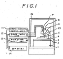
- Figure 1 illustrates a memory reading apparatus according to the present invention.
- a flxed table 2 On an anti-vibration stand 1 there is mounted a flxed table 2 to which an arm 4 is secured.
- a needle operating unit 7 is attached to the arm 4.
- the needle operating unit 7 By turning a dial 6, the needle operating unit 7 is vertically moved for carrying out a Z-axis coarse positional adjustment of a probe tip of an electrically conductive needle 8 relative to a memory 5.
- an X - Y stage 3 and a coarse movement control unit 11 are provided for an X - Y surface coarse movement, over the memory 5, an X - Y stage 3 and a coarse movement control unit 11 are provided.
- An optical micro-scope 25 attached to the arm 4 is used at the time when the needle 8 is coarsely positioned relative to the memory 5.
- Operation of the needle operating unit 7 over the X - Y surface of the memory is carried out by controlling a three dimensional piezo-electric device assembled in the unit 7 with an X- and Y- axis control unit 13.
- Data stored in the memory 5 is read out by a applying, between the memory 5 and the needle 8, a predetermined voltage ranging from 1 to 100 mV.
- the coarse movement control unit 11, a Z-axis control unit 12 and the X- and Y- axis control unit 13 are controlled by a computer 14.
- the computer 14 may be arranged to control the coarse movement control unit 11 and the Z-axis control unit 12 in response to a tunnel effect occurring between a tip portion of the needle 8 and the surface of the memory.
- the tip portion of the needle may, instead of being made of electrically conductive material, be made of semi-conductive material.
- the units precluding a power source, the control units and the computer are housed in a shielded box 24.
- the stage 3 supporting the memory 5, the coarse movement control unit 11 and the optical micro-scope 25 constitute positioning means for positioning the tip portion of the needle 8 close to the surface of the memory 5.
- Scanning means for scanning the tip portion of the needle over the surface of the memory consists of the X- and Y- axis control unit 13.
- Distance controlling means for controlling the distance between the tip portion of the needle and the surface of the memory 5 whilst the tip portion of the needle scans thereover is constituted by the coarse movement control unit 11 and the Z-axis control unit 12.
- the needle 8 is scanned in the X-axis and Y-axis directions on the X - Y surface of the memory 5 to measure the tunnel current.
- FIG. 2 shows the memory 5 consisting of a dielectric material, the data stored therein being read out by the electrically conductive needle 8.
- the memory 5 consists of memory cells 15 to 19 which are made of dielectric material and in which data is stored in the form of polarisation or de-polarisation of the dielectric material.
- a relatively large current flows in the needle when the dielectric material is polarised (see cells 16,18,19) due to the tunnel effect, whereas current flow is less in the case of de-polarisation of the dielectric material (see cells 15,17). In this manner, the reading of data from the memory takes place on an atomic scale.
- Figure 3 shows another form of the memory 5 consisting of an element which is multi-valent, i.e. can have two or more different valencies, the data stored therein being read out by the electrically conductive needle 8.
- the multi-valent element stores data on an atomic scale in the form of a difference in numbers of electric charges that a single atom possesses.
- a relatively large amount of current flows in the needle due to a tunnel effect in the case of atoms 27,29,30, each having a greater number of electric charges.
- the current flow in the needle is lesser in the case of atoms 26,28 each having a lesser number of electric charges.
- the reading of data out of the memory thus takes place on an atomic scale.
- the form of memory 5 shown in Figure 4 consists of a super lattice, the data being read out by using the electrically conductive needle 8.
- the memory consists of cells 31 to 35 and stores data on an atomic scale in the form of the configuration of different types of elements.
- a tunnel current flows.
- the size of an electron cloud is given by the measurement of the tunnel current.
- Each of the different types of elements has a specific size of electron cloud, whereby the reading of data out of the memory thus takes place on an atomic scale.
- Figure 5 shows the memory 5 in the form of an electrically conductive substance, data being stored therein and read out by the electrically conductive needle 8.
- the memory 5 stores data on an atomic scale in the form of differences in film thickness in a direction perpendicular to the memory surface. The film thickness differs depending upon position on the surface of the memory of one to several atoms of an electrically conductive element.
- a tunnel current flows. The level of the tunnel current is a function of distance between the probe tip of the needle and the surface of the memory 5. Therefore, the reading of data out of the memory 5 takes place by measurement of the tunnel current.
- the memory 5 as shown in Figure 6 is in the form of molecules in which the orbit of lone pairs extends in specific directions, data stored therein being read out by the electrically conductive needle 8.
- Data is stored on a molecular scale in the memory 5 with two types of molecules 45 to 50 which have the orbits of localised lone pairs in specific directions.
- the orbits of lone pairs of some of the molecules (see molecules 46,49,51,52) is outwardly directed and others (see molecules 53 to 56) are inwardly directed.
- a relatively large tunnel current flows in the needle when held close to the molecules 46,49 having the orbit of lone pairs directed outwardly, because the potential energy barrier between the needle and the memory is relatively small.
- Another form of the memory 5 (not illustrated) consists of a polar substance immersed in a polar solvent and data stored therein is read out by the electrically conductive needle 8. Data is stored on a molecular scale in the memory 5 with two types of polar substance, one of which is ionized and the other of which is not ionized. When the needle is closely positioned over such a memory, there is a difference in level of tunnel current depending upon whether or not the polar substance is ionized. In this manner, the reading of the data out of the memory takes place on a molecular scale.
- Figure 7 shows a modification of the memory reading apparatus of Figure 1, where the single needle 8 is replaced by a plurality of electrically conductive needles 90. The probe tips of the needles 90 are used to read the memory 5.
- Figure 8 shows the memory 5 consisting of a dielectric material, the data stored therein being read out by the electrically conductive needles 90.
- the memory 5 consists of memory cells 115 to 119 which are made of dielectric material, and in which data is stored in the form of polarisation or de-polarisation of the dielectric material.
- a relatively large current flows in the needles 183,181 which are held close to the polarised dielectric material (see cells 115, 117) due to the tunnel effect, whereas current flow is less in needles 182, 180 which are held close to the de-polarised dielectric material (see cells 116, 118). In this manner, the reading of data from the memory takes place on an atomic scale.
- Figure 9 shows another form of the memory 5 consisting of an element which is multi-valent, i.e. can have two or more different valencies, the data stored therein being read out by the electrically conductive needles 90.
- the multi-valent element stores data on an atomic scale in the form of a difference in numbers of electric charges that a single atom possesses.
- a relatively large tunnel current flows in the needles 183, 181 held close to atoms 126, 128, each having a greater number of electric charges.
- a lesser tunnel current flows in the needles 182, 180 held close to atoms 127, 129 which have a lesser number of electric charges.
- the reading of data out of the memory thus takes place on an atomic scale.
- the form of memory shown in Figure 10 consists of a super lattice, the data being read out by using the electrically conductive needles 90.
- the memory consists of relatively large sized atoms 131, 133 and relatively small sized atoms 132, 134 which can be discriminated by the tunnel current flowing in the needles 90. The reading of data out of the memory thus takes place on an atomic scale.
- Figure 11 shows the memory 5 in the form of an electrically conductive substance, data being stored therein and read out by the electrically conductive needles 90.
- the memory 5 stores data on an atomic scale in the form of differences in film thickness in a direction perpendicular to the memory surface.
- the film thickness differs depending upon position on the surface of the memory of one to several atoms of an electrically conductive element.
- a relatively large tunnel current flows in needles 181, 183 which are held close to portions where the film thickness is larger, whereas a smaller tunnel current flows in needles 180, 182 which are held close to portions where the film thickness is relatively small. Therefore, the reading of data from the memory 5 takes place on an atomic scale.
- the memory 5 as shown in Figure 12 is in the form of molecules in which the orbit of lone pairs extends in specific directions, data stored therein being read out by the electrically conductive needles 90.
- Data is stored on a molecular scale in the memory 5 with two types of molecules which have the orbits of localised lone pairs in specific directions.
- the orbit of lone pairs of some of the molecules is outwardly directed and others are inwardly directed.
- a relatively large tunnel current flows in the needles 183, 181 when held close to molecules 136, 138 having the orbit of lone pairs directed outwardly, because the potential energy barrier between the needles and the memory is relatively small.
- Another form of memory 5 (not illustrated) consists of a polar substance immersed in a polar solvent and data stored therein is read out by the electrically conductive needles 90. Data is stored on a molecular scale in the memory 5 with two types of polar substance, one of which is ionized and the other of which is not ionized. When the needles are closely positioned over such a memory, there is a difference in level of tunnel current depending upon whether or not the polar substance is ionized. In this manner, the reading of data out of the memory takes place on a molecular scale.
- Figure 13 shows another modification of the memory reading apparatus of Figure 1, where the needle 8 is replaced by an electrically conductive needle device 91 having minute needle tips.
- the needle device 91 consists of alternate conductive portions and insulating portions arranged on a semi-conductor substrate, and an electrically conductive needle tip made of one to several atoms attached to the conductive portion.
- This needle device can be produced by minutely shaping an electrically conductive layer grown on a semi-conductor substrate by an etching process.
- Figure 14 shows the memory 5 consisting of a dielectric material, the data stored therein being read out by the electrically conductive needle tips of the needle device 91.
- the memory consists of a dielectric material, in which data is stored in the form of polarisation or de-polarisation of the dielectric material.
- a relatively large current flows in the needle tips 283, 281 when the dielectric material is polarised (see molecules 215, 217) due to the tunnel effect, whereas current flow is less in the case of the needle tips 282, 280 which are held close to the de-polarised dielectric material (see molecules 216, 218).
- reference numerals 290, 291 indicate an insulating portion and a conductive portion of the needle device 91.
- Figure 15 shows another form of the memory 5 consisting of an element which is multi-valent, i.e. can have two or more different valencies, the data stored therein being read out by the electrically conductive needle device 91.
- the multi-valent element stores data on an atomic scale in the form of a difference in numbers of electric charges that a single atom possesses.
- a relatively large current flows, due to the tunnel effect, in needle tips 238, 281 which are close to atoms 226, 228, each having a greater number of electric charges.
- the current flow in the needle tips 282, 280 is less in the case of atoms 227, 229 each having a lesser number of electric charges. The reading of data out of the memory thus takes place on an atomic scale.
- the form of memory 5 shown in Figure 16 consists of a super lattice, the data being read out by using the electrically conductive needle device 91.
- the memory stores data on an atomic scale in the form of the configuration of different types of elements.
- the needle tips 280 to 283 are closely positioned over the surface of the memory, relatively large size atoms 231, 233 and relatively small size atoms 232, 234 can be discriminated from each other due to the tunnel effect.
- the reading of data out of the memory can take place on an atomic scale.
- Figure 17 shows the memory 5 in the form of an electrically conductive substance, data being stored therein and read out by the electrically conductive needle device 91.
- the memory 5 stores data on an atomic scale in the form of differences in film thickness in a direction perpendicular to the memory surface.
- the film thickness differs depending upon position on the surface of the memory of one to several atoms of an electrically conductive element.
- the memory 5 as shown in Figure 18 is in the form of molecules in which the orbit of lone pairs extends in specific directions, data stored therein being read out by the electrically conductive needle device 91.
- Data is stored on a molecular scale in the memory 5 with two types of molecules which have the orbits of localised lone pairs in specific directions.
- the orbit of lone pairs of some of the molecules (see molecules 237, 239, 241) is outwardly directed and others (see molecules 236, 238) are inwardly directed.
- Another form of the memory 5 (not illustrated) consists of a polar substance immersed in a polar solvent and data stored therein is read out by the electrically conductive needle device 91. Data is stored on a molecular scale in the memory 5 with two types of polar substance, one of which is ionized and the other of which is not ionized. When the needle tips are closely positioned over such a memory, there is a difference in the level of tunnel current depending upon whether or not the polar substance is ionized. In this manner, the reading of data out of the memory takes place on a molecular scale.
Abstract
A memory reading apparatus comprises an output section for reading data stored in a memory (5) comprising at least one needle (8) having a fine tip portion. Positioning means (3, 11, 25) position a tip portion of the needle (8) close to the surface of the memory (5). Scanning means (13) scan the tip portion over the surface of the memory (5) and distance controlling means (11, 12) control the distance between the tip portion and the surface of the memory whilst the tip portion scans thereover.
Description
- This invention relates to memory reading apparatus. In conventional memory reading devices, a magnetic head has been used for reading a memory composed of magnetically recorded media, such as floppy disks, magnetic tapes, and an optical head has been used for media such as optical disks, opto-magnetic disks, etc. A problem exists with such heads in that the memory cannot withstand long term use due to physical contact of the head with the memory. A further problem exists in that very large amounts of data cannot be stored in the memory unless memory cells are made up of a predetermined number of atoms or molecules.
- The present invention seeks to provide a memory reading apparatus which enables non-contact reading on an atomic or molecular scale.
- According to the present invention, there is provided a memory reading apparatus characterised by comprising an output section for reading data stored in a memory, said output section comprising at least one needle means having a fine tip portion; and control means for controlling the output section, said control means comprising positioning means for positioning a tip portion of the needle means close to a surface of the memory, means for scanning the tip portion over the surface of the memory and distance controlling means for controlling a distance between the tip portion and the surface of the memory whilst the tip portion scans thereover.
- Preferably the distance between the tip portion of the needle means and the surface of the memory is maintained so as to cause a tunnel effect.
- The distance controlling means may be operative in response to the tunnel effect occurring between the tip portion of the needle means and the surface of the memory.
- The needle means may be manufactured by semi-conductor processing techniques.
- The positioning means may comprise an X - Y stage, a coarse control section for positioning in an X - Y plane, and an optical micro-scope for examining the distance between the tip portion of the needle means and the surface of the memory. The distance controlling means may comprise a coarse control section and a Z-axis control section.
- The invention is illustrated, merely by way of example, in the accompanying drawings, in which:
- Figure 1 is a schematic diagram of one embodiment of a memory reading apparatus according to the present invention;
- Figures 2 to 6 are enlarged schematic diagrams illustrating various forms of memory for the memory reading apparatus of Figure 1;
- Figure 7 shows a modification of the memory reading apparatus of Figure 1;
- Figures 8 to 12 are enlarged schematic diagrams illustrating various forms of memory of the memory reading apparatus of Figure 7;
- Figure 13 shows a further modification of the memory reading apparatus of Figure 1; and
- Figures 14 to 18 are enlarged schematic diagrams illustrating various forms of memory for the memory reading apparatus of Figure 13.
- Figure 1 illustrates a memory reading apparatus according to the present invention. On an
anti-vibration stand 1 there is mounted a flxed table 2 to which anarm 4 is secured. Aneedle operating unit 7 is attached to thearm 4. By turning adial 6, theneedle operating unit 7 is vertically moved for carrying out a Z-axis coarse positional adjustment of a probe tip of an electricallyconductive needle 8 relative to amemory 5. For an X - Y surface coarse movement, over thememory 5, an X -Y stage 3 and a coarsemovement control unit 11 are provided. Anoptical micro-scope 25 attached to thearm 4 is used at the time when theneedle 8 is coarsely positioned relative to thememory 5. Operation of theneedle operating unit 7 over the X - Y surface of the memory is carried out by controlling a three dimensional piezo-electric device assembled in theunit 7 with an X- and Y-axis control unit 13. Data stored in thememory 5 is read out by a applying, between thememory 5 and theneedle 8, a predetermined voltage ranging from 1 to 100 mV. The coarsemovement control unit 11, a Z-axis control unit 12 and the X- and Y-axis control unit 13 are controlled by acomputer 14. For example, thecomputer 14 may be arranged to control the coarsemovement control unit 11 and the Z-axis control unit 12 in response to a tunnel effect occurring between a tip portion of theneedle 8 and the surface of the memory. The tip portion of the needle may, instead of being made of electrically conductive material, be made of semi-conductive material. The units precluding a power source, the control units and the computer are housed in a shieldedbox 24. - The
stage 3 supporting thememory 5, the coarsemovement control unit 11 and theoptical micro-scope 25 constitute positioning means for positioning the tip portion of theneedle 8 close to the surface of thememory 5. Scanning means for scanning the tip portion of the needle over the surface of the memory consists of the X- and Y-axis control unit 13. Distance controlling means for controlling the distance between the tip portion of the needle and the surface of thememory 5 whilst the tip portion of the needle scans thereover is constituted by the coarsemovement control unit 11 and the Z-axis control unit 12. In operation, theneedle 8 is scanned in the X-axis and Y-axis directions on the X - Y surface of thememory 5 to measure the tunnel current. - Figure 2 shows the
memory 5 consisting of a dielectric material, the data stored therein being read out by the electricallyconductive needle 8. Thememory 5 consists ofmemory cells 15 to 19 which are made of dielectric material and in which data is stored in the form of polarisation or de-polarisation of the dielectric material. When the needle is closely positioned over the surface of thememory 5, a relatively large current flows in the needle when the dielectric material is polarised (seecells cells 15,17). In this manner, the reading of data from the memory takes place on an atomic scale. - Figure 3 shows another form of the
memory 5 consisting of an element which is multi-valent, i.e. can have two or more different valencies, the data stored therein being read out by the electricallyconductive needle 8. The multi-valent element stores data on an atomic scale in the form of a difference in numbers of electric charges that a single atom possesses. When the needle is closely positioned over the surface of thememory 5, a relatively large amount of current flows in the needle due to a tunnel effect in the case ofatoms 27,29,30, each having a greater number of electric charges. On the other hand, the current flow in the needle is lesser in the case of atoms 26,28 each having a lesser number of electric charges. The reading of data out of the memory thus takes place on an atomic scale. - The form of
memory 5 shown in Figure 4 consists of a super lattice, the data being read out by using the electricallyconductive needle 8. The memory consists ofcells 31 to 35 and stores data on an atomic scale in the form of the configuration of different types of elements. When the needle is closely positioned over the surface of the memory, a tunnel current flows. The size of an electron cloud is given by the measurement of the tunnel current. Each of the different types of elements has a specific size of electron cloud, whereby the reading of data out of the memory thus takes place on an atomic scale. - Figure 5 shows the
memory 5 in the form of an electrically conductive substance, data being stored therein and read out by the electricallyconductive needle 8. Thememory 5 stores data on an atomic scale in the form of differences in film thickness in a direction perpendicular to the memory surface. The film thickness differs depending upon position on the surface of the memory of one to several atoms of an electrically conductive element. When the needle is closely positioned over the surface of thememory 5, a tunnel current flows. The level of the tunnel current is a function of distance between the probe tip of the needle and the surface of thememory 5. Therefore, the reading of data out of thememory 5 takes place by measurement of the tunnel current. - The
memory 5 as shown in Figure 6 is in the form of molecules in which the orbit of lone pairs extends in specific directions, data stored therein being read out by the electricallyconductive needle 8. Data is stored on a molecular scale in thememory 5 with two types of molecules 45 to 50 which have the orbits of localised lone pairs in specific directions. The orbits of lone pairs of some of the molecules (seemolecules molecules 53 to 56) are inwardly directed. When the needle is closely positioned over the surface of thememory 5, a relatively large tunnel current flows in the needle when held close to themolecules - Another form of the memory 5 (not illustrated) consists of a polar substance immersed in a polar solvent and data stored therein is read out by the electrically
conductive needle 8. Data is stored on a molecular scale in thememory 5 with two types of polar substance, one of which is ionized and the other of which is not ionized. When the needle is closely positioned over such a memory, there is a difference in level of tunnel current depending upon whether or not the polar substance is ionized. In this manner, the reading of the data out of the memory takes place on a molecular scale. - Figure 7 shows a modification of the memory reading apparatus of Figure 1, where the
single needle 8 is replaced by a plurality of electrically conductive needles 90. The probe tips of the needles 90 are used to read thememory 5. - Figure 8 shows the
memory 5 consisting of a dielectric material, the data stored therein being read out by the electrically conductive needles 90. Thememory 5 consists ofmemory cells 115 to 119 which are made of dielectric material, and in which data is stored in the form of polarisation or de-polarisation of the dielectric material. When the needles are closely positioned over the surface of thememory 5, a relatively large current flows in the needles 183,181 which are held close to the polarised dielectric material (seecells 115, 117) due to the tunnel effect, whereas current flow is less inneedles cells 116, 118). In this manner, the reading of data from the memory takes place on an atomic scale. - Figure 9 shows another form of the
memory 5 consisting of an element which is multi-valent, i.e. can have two or more different valencies, the data stored therein being read out by the electrically conductive needles 90. The multi-valent element stores data on an atomic scale in the form of a difference in numbers of electric charges that a single atom possesses. When the needles are closely positioned over the surface of thememory 5, a relatively large tunnel current flows in theneedles atoms 126, 128, each having a greater number of electric charges. On the other hand, a lesser tunnel current flows in theneedles atoms - The form of memory shown in Figure 10 consists of a super lattice, the data being read out by using the electrically conductive needles 90. The memory consists of relatively large
sized atoms sized atoms - Figure 11 shows the
memory 5 in the form of an electrically conductive substance, data being stored therein and read out by the electrically conductive needles 90. Thememory 5 stores data on an atomic scale in the form of differences in film thickness in a direction perpendicular to the memory surface. The film thickness differs depending upon position on the surface of the memory of one to several atoms of an electrically conductive element. When the needles are closely positioned over the surface of thememory 5, a relatively large tunnel current flows inneedles needles memory 5 takes place on an atomic scale. - The
memory 5 as shown in Figure 12 is in the form of molecules in which the orbit of lone pairs extends in specific directions, data stored therein being read out by the electrically conductive needles 90. Data is stored on a molecular scale in thememory 5 with two types of molecules which have the orbits of localised lone pairs in specific directions. The orbit of lone pairs of some of the molecules is outwardly directed and others are inwardly directed. When the needles are closely positioned over the surface of thememory 5, a relatively large tunnel current flows in theneedles molecules molecules - Another form of memory 5 (not illustrated) consists of a polar substance immersed in a polar solvent and data stored therein is read out by the electrically conductive needles 90. Data is stored on a molecular scale in the
memory 5 with two types of polar substance, one of which is ionized and the other of which is not ionized. When the needles are closely positioned over such a memory, there is a difference in level of tunnel current depending upon whether or not the polar substance is ionized. In this manner, the reading of data out of the memory takes place on a molecular scale. - Figure 13 shows another modification of the memory reading apparatus of Figure 1, where the
needle 8 is replaced by an electricallyconductive needle device 91 having minute needle tips. Theneedle device 91 consists of alternate conductive portions and insulating portions arranged on a semi-conductor substrate, and an electrically conductive needle tip made of one to several atoms attached to the conductive portion. This needle device can be produced by minutely shaping an electrically conductive layer grown on a semi-conductor substrate by an etching process. - Figure 14 shows the
memory 5 consisting of a dielectric material, the data stored therein being read out by the electrically conductive needle tips of theneedle device 91. The memory consists of a dielectric material, in which data is stored in the form of polarisation or de-polarisation of the dielectric material. When the needle tips are closely positioned over one of the dielectric molecules on the surface of thememory 5, a relatively large current flows in theneedle tips molecules 215, 217) due to the tunnel effect, whereas current flow is less in the case of theneedle tips molecules 216, 218). In this manner, the reading of data from the memory takes place on an atomic scale. In Figure 14reference numerals needle device 91. - Figure 15 shows another form of the
memory 5 consisting of an element which is multi-valent, i.e. can have two or more different valencies, the data stored therein being read out by the electricallyconductive needle device 91. The multi-valent element stores data on an atomic scale in the form of a difference in numbers of electric charges that a single atom possesses. When the needle tips are closely positioned over the surface of thememory 5, a relatively large current flows, due to the tunnel effect, inneedle tips atoms needle tips atoms - The form of
memory 5 shown in Figure 16 consists of a super lattice, the data being read out by using the electricallyconductive needle device 91. The memory stores data on an atomic scale in the form of the configuration of different types of elements. When theneedle tips 280 to 283 are closely positioned over the surface of the memory, relativelylarge size atoms small size atoms - Figure 17 shows the
memory 5 in the form of an electrically conductive substance, data being stored therein and read out by the electricallyconductive needle device 91. Thememory 5 stores data on an atomic scale in the form of differences in film thickness in a direction perpendicular to the memory surface. The film thickness differs depending upon position on the surface of the memory of one to several atoms of an electrically conductive element. When a needle tip is closely positioned over the surface of thememory 5, a relatively large tunnel current flows in theneedle tips needle tips memory 5 takes place by measurement of the tunnel current. - The
memory 5 as shown in Figure 18 is in the form of molecules in which the orbit of lone pairs extends in specific directions, data stored therein being read out by the electricallyconductive needle device 91. Data is stored on a molecular scale in thememory 5 with two types of molecules which have the orbits of localised lone pairs in specific directions. The orbit of lone pairs of some of the molecules (seemolecules 237, 239, 241) is outwardly directed and others (seemolecules 236, 238) are inwardly directed. When theneedle tips memory 5 close to themolecules molecules needle tips molecules 237, 239, each having the orbit of lone pairs directed inwardly, because the potential energy barrier therebetween is relatively large. In this manner, reading of data on a molecular scale takes place. - Another form of the memory 5 (not illustrated) consists of a polar substance immersed in a polar solvent and data stored therein is read out by the electrically
conductive needle device 91. Data is stored on a molecular scale in thememory 5 with two types of polar substance, one of which is ionized and the other of which is not ionized. When the needle tips are closely positioned over such a memory, there is a difference in the level of tunnel current depending upon whether or not the polar substance is ionized. In this manner, the reading of data out of the memory takes place on a molecular scale.
Claims (12)
1. A memory reading apparatus characterised by comprising an output section for reading data stored in a memory (5), said output section comprising at least one needle means (8,90,91) having a fine tip portion; and control means for controlling the output section, said control means comprising positioning means (3,11,25) for positioning a tip portion of the needle means close to a surface of the memory (5), means (13) for scanning the tip portion over the surface of the memory (5) and distance controlling means (11,12) for controlling a distance between the tip portion and the surface of the memory whilst the tip portion scans thereover.
2. A memory reading apparatus as claimed in claim 1, characterised in that the distance between the tip portion of the needle means (8,90,91) and the surface of the memory (5) is maintained so as to cause a tunnel effect.
3. A memory reading apparatus as claimed in claim 2, characterised in that the distance controlling means (11,12) is operative in response to the tunnel effect occurring between the tip portion of the needle means (8,90,91) and the surface of the memory (5).
4. A memory reading apparatus as claimed in any preceding claim characterised in that the needle means (91) is manufactured by semi-conductor processing techniques.
5. A memory reading apparatus as claimed in any preceding claim characterised in that a dielectric material is used as the memory (5).
6. A memory reading apparatus as claimed in any of claims 1 to 4 characterised in that a multi-valent element is used as the memory (5).
7. A memory reading apparatus as claimed in any of claims 1 to 4 characterised in that a super lattice in which elements of different kinds are configured is used as the memory (5).
8. A memory reading apparatus as claimed in any of claims 1 to 4 characterised in that a film whose thickness differs depending upon position is used as the memory (5).
9. A memory reading apparatus as claimed in any of claims 1 to 4 characterised in that molecules whose orbit of lone pairs extends in specific directions is used as the memory (5).
10. A memory reading apparatus as claimed in any of claims 1 to 4 characterised in that a polar compound which is immersed in a polar solvent is used as the memory (5).
11. A memory reading apparatus as claimed in any preceding claim characterised in that the positioning means comprises an X - Y stage (3), a coarse control section (11) for positioning in an X - Y plane, and an optical micro-scope (25) for examining the distance between the tip portion of the needle means and the surface of the memory (5).
12. A memory reading apparatus as claimed in any preceding claim characterised in that the distance controlling means comprises a coarse control section (11) and a Z-axis control section (12).
Applications Claiming Priority (6)
| Application Number | Priority Date | Filing Date | Title |
|---|---|---|---|
| JP22736587A JPS6470942A (en) | 1987-09-10 | 1987-09-10 | Memory output device |
| JP227365/87 | 1987-09-10 | ||
| JP247152/87 | 1987-09-30 | ||
| JP24715287A JPH0191339A (en) | 1987-09-30 | 1987-09-30 | Memory output device |
| JP62253156A JP2673351B2 (en) | 1987-10-07 | 1987-10-07 | Memory output device |
| JP253156/87 | 1987-10-07 |
Publications (2)
| Publication Number | Publication Date |
|---|---|
| EP0307211A2 true EP0307211A2 (en) | 1989-03-15 |
| EP0307211A3 EP0307211A3 (en) | 1991-05-15 |
Family
ID=27331278
Family Applications (1)
| Application Number | Title | Priority Date | Filing Date |
|---|---|---|---|
| EP19880308325 Withdrawn EP0307211A3 (en) | 1987-09-10 | 1988-09-09 | Memory reading device |
Country Status (2)
| Country | Link |
|---|---|
| US (1) | US4962480A (en) |
| EP (1) | EP0307211A3 (en) |
Cited By (15)
| Publication number | Priority date | Publication date | Assignee | Title |
|---|---|---|---|---|
| EP0334677A1 (en) * | 1988-03-25 | 1989-09-27 | Canon Kabushiki Kaisha | Information recording device and information recording and reproducing process |
| EP0394995A2 (en) * | 1989-04-25 | 1990-10-31 | Canon Kabushiki Kaisha | Information record/reproducing apparatus and information recording medium |
| EP0416920A2 (en) * | 1989-09-07 | 1991-03-13 | Canon Kabushiki Kaisha | Information processing method and information processing device |
| EP0497288A2 (en) * | 1991-01-29 | 1992-08-05 | Canon Kabushiki Kaisha | Probe scanning system |
| WO1994002939A1 (en) * | 1992-07-17 | 1994-02-03 | The Penn State Research Foundation | Reading and writing stored information by means of electrochemistry |
| US5434842A (en) * | 1992-07-17 | 1995-07-18 | Biotechnology Research And Development Corporation | Reading and writing stored information by means of electrochemistry |
| US5623476A (en) * | 1986-12-24 | 1997-04-22 | Canon Kabushiki Kaisha | Recording device and reproduction device |
| US6208553B1 (en) | 1999-07-01 | 2001-03-27 | The Regents Of The University Of California | High density non-volatile memory device incorporating thiol-derivatized porphyrins |
| US6212093B1 (en) | 2000-01-14 | 2001-04-03 | North Carolina State University | High-density non-volatile memory devices incorporating sandwich coordination compounds |
| US6272038B1 (en) | 2000-01-14 | 2001-08-07 | North Carolina State University | High-density non-volatile memory devices incorporating thiol-derivatized porphyrin trimers |
| US6381169B1 (en) | 1999-07-01 | 2002-04-30 | The Regents Of The University Of California | High density non-volatile memory device |
| US6728129B2 (en) | 2002-02-19 | 2004-04-27 | The Regents Of The University Of California | Multistate triple-decker dyads in three distinct architectures for information storage applications |
| US6777516B2 (en) | 2000-01-14 | 2004-08-17 | North Carolina State University | Substrates carrying polymers of linked sandwich coordination compounds and methods of use thereof |
| US6921475B2 (en) | 2001-03-23 | 2005-07-26 | The Regents Of The University Of California | Open circuit potential amperometry and voltammetry |
| US7042755B1 (en) | 1999-07-01 | 2006-05-09 | The Regents Of The University Of California | High density non-volatile memory device |
Families Citing this family (34)
| Publication number | Priority date | Publication date | Assignee | Title |
|---|---|---|---|---|
| US5257024A (en) * | 1988-05-26 | 1993-10-26 | Quan-Scan, Inc. | Search position encoder |
| CA2000071C (en) * | 1988-10-04 | 1997-01-28 | Haruki Kawada | Recording and reproducing apparatus and recording and reproducing method and recording medium for the recording and reproducing method |
| US5289408A (en) * | 1989-02-09 | 1994-02-22 | Olympus Optical Co., Ltd. | Memory apparatus using tunnel current techniques |
| US5144581A (en) * | 1989-02-09 | 1992-09-01 | Olympus Optical Co., Ltd. | Apparatus including atomic probes utilizing tunnel current to read, write and erase data |
| JP2909829B2 (en) * | 1989-07-05 | 1999-06-23 | セイコーインスツルメンツ株式会社 | Compound scanning tunneling microscope with alignment function |
| JP2859715B2 (en) * | 1989-08-10 | 1999-02-24 | キヤノン株式会社 | Recording medium substrate and manufacturing method thereof, recording medium, recording method, recording / reproducing method, recording apparatus, recording / reproducing apparatus |
| CA2021582A1 (en) * | 1989-08-30 | 1991-03-01 | Harris A. Goldberg | Scanning tunneling microscope utilizing optical fluorescent for reading |
| US5051977A (en) * | 1989-08-30 | 1991-09-24 | Hoechst Celanese Corp. | Scanning tunneling microscope memory utilizing optical fluorescence of substrate for reading |
| JPH041949A (en) * | 1990-04-18 | 1992-01-07 | Canon Inc | Information input and/or output device |
| JP2761801B2 (en) * | 1990-10-04 | 1998-06-04 | キヤノン株式会社 | Angular positional relationship detection method and encoder using the same |
| US5216631A (en) * | 1990-11-02 | 1993-06-01 | Sliwa Jr John W | Microvibratory memory device |
| WO1992012528A1 (en) * | 1991-01-11 | 1992-07-23 | Hitachi Limited | Surface atom machining method and apparatus |
| US5166919A (en) * | 1991-07-11 | 1992-11-24 | International Business Machines Corporation | Atomic scale electronic switch |
| US5155361A (en) * | 1991-07-26 | 1992-10-13 | The Arizona Board Of Regents, A Body Corporate Acting For And On Behalf Of Arizona State University | Potentiostatic preparation of molecular adsorbates for scanning probe microscopy |
| US5453970A (en) * | 1993-07-13 | 1995-09-26 | Rust; Thomas F. | Molecular memory medium and molecular memory disk drive for storing information using a tunnelling probe |
| US5440920A (en) * | 1994-02-03 | 1995-08-15 | Molecular Imaging Systems | Scanning force microscope with beam tracking lens |
| US5866805A (en) * | 1994-05-19 | 1999-02-02 | Molecular Imaging Corporation Arizona Board Of Regents | Cantilevers for a magnetically driven atomic force microscope |
| US5753814A (en) * | 1994-05-19 | 1998-05-19 | Molecular Imaging Corporation | Magnetically-oscillated probe microscope for operation in liquids |
| US5513518A (en) * | 1994-05-19 | 1996-05-07 | Molecular Imaging Corporation | Magnetic modulation of force sensor for AC detection in an atomic force microscope |
| US5515719A (en) * | 1994-05-19 | 1996-05-14 | Molecular Imaging Corporation | Controlled force microscope for operation in liquids |
| US5615143A (en) * | 1994-09-19 | 1997-03-25 | Cornell Research Foundation, Inc. | Optomechanical terabit data storage system |
| KR100265692B1 (en) * | 1997-07-03 | 2000-09-15 | 윤덕용 | Non-volatile memory and non-volatile memory operation method using afm |
| US7260051B1 (en) | 1998-12-18 | 2007-08-21 | Nanochip, Inc. | Molecular memory medium and molecular memory integrated circuit |
| US6562633B2 (en) * | 2001-02-26 | 2003-05-13 | International Business Machines Corporation | Assembling arrays of small particles using an atomic force microscope to define ferroelectric domains |
| US20040150472A1 (en) * | 2002-10-15 | 2004-08-05 | Rust Thomas F. | Fault tolerant micro-electro mechanical actuators |
| US6985377B2 (en) * | 2002-10-15 | 2006-01-10 | Nanochip, Inc. | Phase change media for high density data storage |
| US6982898B2 (en) * | 2002-10-15 | 2006-01-03 | Nanochip, Inc. | Molecular memory integrated circuit utilizing non-vibrating cantilevers |
| US7233517B2 (en) | 2002-10-15 | 2007-06-19 | Nanochip, Inc. | Atomic probes and media for high density data storage |
| US7301887B2 (en) | 2004-04-16 | 2007-11-27 | Nanochip, Inc. | Methods for erasing bit cells in a high density data storage device |
| US20050232061A1 (en) | 2004-04-16 | 2005-10-20 | Rust Thomas F | Systems for writing and reading highly resolved domains for high density data storage |
| US7379412B2 (en) | 2004-04-16 | 2008-05-27 | Nanochip, Inc. | Methods for writing and reading highly resolved domains for high density data storage |
| US7463573B2 (en) | 2005-06-24 | 2008-12-09 | Nanochip, Inc. | Patterned media for a high density data storage device |
| US7367119B2 (en) | 2005-06-24 | 2008-05-06 | Nanochip, Inc. | Method for forming a reinforced tip for a probe storage device |
| US7309630B2 (en) | 2005-07-08 | 2007-12-18 | Nanochip, Inc. | Method for forming patterned media for a high density data storage device |
Citations (5)
| Publication number | Priority date | Publication date | Assignee | Title |
|---|---|---|---|---|
| US3683337A (en) * | 1969-11-24 | 1972-08-08 | Texas Instruments Inc | Information storage by changing the valence state of a semi-conductor crystal |
| US4489278A (en) * | 1982-06-03 | 1984-12-18 | Tokyo Shibaura Denki Kabushiki Kaisha | Electrostatic voltage detecting device |
| US4575822A (en) * | 1983-02-15 | 1986-03-11 | The Board Of Trustees Of The Leland Stanford Junior University | Method and means for data storage using tunnel current data readout |
| US4618767A (en) * | 1985-03-22 | 1986-10-21 | International Business Machines Corporation | Low-energy scanning transmission electron microscope |
| GB2182480A (en) * | 1985-10-31 | 1987-05-13 | Emi Plc Thorn | Information recovery system |
Family Cites Families (2)
| Publication number | Priority date | Publication date | Assignee | Title |
|---|---|---|---|---|
| US4829507A (en) * | 1984-09-14 | 1989-05-09 | Xerox Corporation | Method of and system for atomic scale readout of recorded information |
| US4826732A (en) * | 1987-03-16 | 1989-05-02 | Xerox Corporation | Recording medium |
-
1988
- 1988-09-09 EP EP19880308325 patent/EP0307211A3/en not_active Withdrawn
- 1988-09-12 US US07/243,514 patent/US4962480A/en not_active Expired - Lifetime
Patent Citations (5)
| Publication number | Priority date | Publication date | Assignee | Title |
|---|---|---|---|---|
| US3683337A (en) * | 1969-11-24 | 1972-08-08 | Texas Instruments Inc | Information storage by changing the valence state of a semi-conductor crystal |
| US4489278A (en) * | 1982-06-03 | 1984-12-18 | Tokyo Shibaura Denki Kabushiki Kaisha | Electrostatic voltage detecting device |
| US4575822A (en) * | 1983-02-15 | 1986-03-11 | The Board Of Trustees Of The Leland Stanford Junior University | Method and means for data storage using tunnel current data readout |
| US4618767A (en) * | 1985-03-22 | 1986-10-21 | International Business Machines Corporation | Low-energy scanning transmission electron microscope |
| GB2182480A (en) * | 1985-10-31 | 1987-05-13 | Emi Plc Thorn | Information recovery system |
Non-Patent Citations (1)
| Title |
|---|
| REVIEW OF SCIENTIFIC INSTRUMENTS. vol. 57, no. 2, February 1986, NEW YORK US pages 221 - 224; C.GERBER ET AL: "Scanning Tunneling microscope combined with a scanning electron microscope" * |
Cited By (27)
| Publication number | Priority date | Publication date | Assignee | Title |
|---|---|---|---|---|
| US5623476A (en) * | 1986-12-24 | 1997-04-22 | Canon Kabushiki Kaisha | Recording device and reproduction device |
| EP0334677A1 (en) * | 1988-03-25 | 1989-09-27 | Canon Kabushiki Kaisha | Information recording device and information recording and reproducing process |
| US5812516A (en) * | 1988-03-25 | 1998-09-22 | Canon Kabushiki Kaisha | Maintaining interatomic distance between an STM probe and a recording layer |
| EP0394995A3 (en) * | 1989-04-25 | 1993-03-31 | Canon Kabushiki Kaisha | Information record/reproducing apparatus and information recording medium |
| US5581537A (en) * | 1989-04-25 | 1996-12-03 | Canon Kabushiki Kaisha | Information record/reproducing apparatus and information recording medium |
| EP0394995A2 (en) * | 1989-04-25 | 1990-10-31 | Canon Kabushiki Kaisha | Information record/reproducing apparatus and information recording medium |
| US5182724A (en) * | 1989-09-07 | 1993-01-26 | Canon Kabushiki Kaisha | Information processing method and information processing device |
| EP0416920A3 (en) * | 1989-09-07 | 1992-05-13 | Canon Kabushiki Kaisha | Information processing method and information processing device |
| EP0416920A2 (en) * | 1989-09-07 | 1991-03-13 | Canon Kabushiki Kaisha | Information processing method and information processing device |
| EP0497288A2 (en) * | 1991-01-29 | 1992-08-05 | Canon Kabushiki Kaisha | Probe scanning system |
| EP0497288A3 (en) * | 1991-01-29 | 1993-04-14 | Canon Kabushiki Kaisha | Probe scanning system |
| US5414690A (en) * | 1991-01-29 | 1995-05-09 | Canon Kabushiki Kaisha | Moving apparatus, a moving method and an information detection and/or input apparatus using the same |
| WO1994002939A1 (en) * | 1992-07-17 | 1994-02-03 | The Penn State Research Foundation | Reading and writing stored information by means of electrochemistry |
| US5434842A (en) * | 1992-07-17 | 1995-07-18 | Biotechnology Research And Development Corporation | Reading and writing stored information by means of electrochemistry |
| US6208553B1 (en) | 1999-07-01 | 2001-03-27 | The Regents Of The University Of California | High density non-volatile memory device incorporating thiol-derivatized porphyrins |
| US6381169B1 (en) | 1999-07-01 | 2002-04-30 | The Regents Of The University Of California | High density non-volatile memory device |
| US6657884B2 (en) | 1999-07-01 | 2003-12-02 | The Regents Of The University Of California | High density non-volatile memory device |
| US7042755B1 (en) | 1999-07-01 | 2006-05-09 | The Regents Of The University Of California | High density non-volatile memory device |
| US7061791B2 (en) | 1999-07-01 | 2006-06-13 | The Regents Of The University Of California | High density molecular memory device |
| US7518905B2 (en) | 1999-07-01 | 2009-04-14 | The Regents Of The University Of California | High density memory device |
| US6212093B1 (en) | 2000-01-14 | 2001-04-03 | North Carolina State University | High-density non-volatile memory devices incorporating sandwich coordination compounds |
| US6272038B1 (en) | 2000-01-14 | 2001-08-07 | North Carolina State University | High-density non-volatile memory devices incorporating thiol-derivatized porphyrin trimers |
| US6451942B1 (en) | 2000-01-14 | 2002-09-17 | North Carolina State University | Substrates carrying polymers of linked sandwich coordination compounds and methods of use thereof |
| US6777516B2 (en) | 2000-01-14 | 2004-08-17 | North Carolina State University | Substrates carrying polymers of linked sandwich coordination compounds and methods of use thereof |
| US6921475B2 (en) | 2001-03-23 | 2005-07-26 | The Regents Of The University Of California | Open circuit potential amperometry and voltammetry |
| US7826250B2 (en) | 2001-03-23 | 2010-11-02 | North Carolina State Univeristy | Open circuit potential amperometry and voltammetry |
| US6728129B2 (en) | 2002-02-19 | 2004-04-27 | The Regents Of The University Of California | Multistate triple-decker dyads in three distinct architectures for information storage applications |
Also Published As
| Publication number | Publication date |
|---|---|
| EP0307211A3 (en) | 1991-05-15 |
| US4962480A (en) | 1990-10-09 |
Similar Documents
| Publication | Publication Date | Title |
|---|---|---|
| EP0307211A2 (en) | Memory reading device | |
| EP0307210A2 (en) | Memory writing apparatus | |
| JP2628790B2 (en) | Method and apparatus for storing digital information in the form of stored charges | |
| US5278704A (en) | Information processing apparatus including magnetic material having a predetermined magnetization pattern with respect to a recording medium | |
| EP0478666B1 (en) | Microfabricated microscope assembly | |
| US5107112A (en) | Scanning tunnel-current-detecting device and method for detecting tunnel current and scanning tunnelling microscope and recording/reproducing device using thereof | |
| US5220555A (en) | Scanning tunnel-current-detecting device and method for detecting tunnel current and scanning tunnelling microscope and recording/reproducing device using thereof | |
| KR19990082262A (en) | Microscopic imaging device for physical properties of objects at room temperature | |
| KR100407202B1 (en) | Methods and devices for measuring real-time position in nanometers of sensors in scanning tunneling microscopes or other sensors that scan atomic or other wavy surfaces | |
| US5214342A (en) | Two-dimensional walker assembly for a scanning tunneling microscope | |
| EP0431623B1 (en) | Method and Apparatus for Forming a Probe | |
| US5130554A (en) | Two-dimensional scanning device for detecting position between two relatively movable objects | |
| Gehrtz et al. | Scanning tunneling microscopy of machined surfaces | |
| JP2673351B2 (en) | Memory output device | |
| KR100264634B1 (en) | Storage device and how to delete the information stored therein | |
| JP2673352B2 (en) | Memory input device | |
| JP3053971B2 (en) | Three-dimensional displacement element for generating tunnel current, multi-tip unit using the three-dimensional displacement element for generating tunnel current, and information processing apparatus | |
| US6208151B1 (en) | Method and apparatus for measurement of microscopic electrical characteristics | |
| JPH0191339A (en) | Memory output device | |
| Nagaishi et al. | HTS SQUID microscope head with permalloy flux guide | |
| JP2995126B2 (en) | Information processing device | |
| JPH07110969A (en) | Face alignment method, position control mechanism and information processor with the mechanism | |
| Foubister et al. | Scanning Tunneling Microscopy | |
| JPH04223203A (en) | Cantilever type probe and information processing device and method using it | |
| Sexton | Scanning Tunnelling Microscopy |
Legal Events
| Date | Code | Title | Description |
|---|---|---|---|
| PUAI | Public reference made under article 153(3) epc to a published international application that has entered the european phase |
Free format text: ORIGINAL CODE: 0009012 |
|
| AK | Designated contracting states |
Kind code of ref document: A2 Designated state(s): DE FR GB |
|
| PUAL | Search report despatched |
Free format text: ORIGINAL CODE: 0009013 |
|
| AK | Designated contracting states |
Kind code of ref document: A3 Designated state(s): DE FR GB |
|
| STAA | Information on the status of an ep patent application or granted ep patent |
Free format text: STATUS: THE APPLICATION IS DEEMED TO BE WITHDRAWN |
|
| 18D | Application deemed to be withdrawn |
Effective date: 19911116 |