EP0310302A2 - Multipurpose socket - Google Patents
Multipurpose socket Download PDFInfo
- Publication number
- EP0310302A2 EP0310302A2 EP88308813A EP88308813A EP0310302A2 EP 0310302 A2 EP0310302 A2 EP 0310302A2 EP 88308813 A EP88308813 A EP 88308813A EP 88308813 A EP88308813 A EP 88308813A EP 0310302 A2 EP0310302 A2 EP 0310302A2
- Authority
- EP
- European Patent Office
- Prior art keywords
- tape
- contact
- connector
- area
- circuit board
- Prior art date
- Legal status (The legal status is an assumption and is not a legal conclusion. Google has not performed a legal analysis and makes no representation as to the accuracy of the status listed.)
- Granted
Links
Images

Classifications
-
- G—PHYSICS
- G01—MEASURING; TESTING
- G01R—MEASURING ELECTRIC VARIABLES; MEASURING MAGNETIC VARIABLES
- G01R1/00—Details of instruments or arrangements of the types included in groups G01R5/00 - G01R13/00 and G01R31/00
- G01R1/02—General constructional details
- G01R1/04—Housings; Supporting members; Arrangements of terminals
-
- H—ELECTRICITY
- H05—ELECTRIC TECHNIQUES NOT OTHERWISE PROVIDED FOR
- H05K—PRINTED CIRCUITS; CASINGS OR CONSTRUCTIONAL DETAILS OF ELECTRIC APPARATUS; MANUFACTURE OF ASSEMBLAGES OF ELECTRICAL COMPONENTS
- H05K7/00—Constructional details common to different types of electric apparatus
- H05K7/02—Arrangements of circuit components or wiring on supporting structure
- H05K7/10—Plug-in assemblages of components, e.g. IC sockets
- H05K7/1053—Plug-in assemblages of components, e.g. IC sockets having interior leads
- H05K7/1061—Plug-in assemblages of components, e.g. IC sockets having interior leads co-operating by abutting
-
- G—PHYSICS
- G01—MEASURING; TESTING
- G01R—MEASURING ELECTRIC VARIABLES; MEASURING MAGNETIC VARIABLES
- G01R1/00—Details of instruments or arrangements of the types included in groups G01R5/00 - G01R13/00 and G01R31/00
- G01R1/02—General constructional details
- G01R1/04—Housings; Supporting members; Arrangements of terminals
- G01R1/0408—Test fixtures or contact fields; Connectors or connecting adaptors; Test clips; Test sockets
- G01R1/0433—Sockets for IC's or transistors
- G01R1/0475—Sockets for IC's or transistors for TAB IC's
Definitions
- This invention relates to an improvement in devices for electrically testing high performance integrated circuit devices or chips, and in one aspect to an improved test socket for supporting the chip, whether on tape or not, free of detrimental effect on the device or tape and affording rapid facile positive electrical connection with the contact points of said device.
- chips to provide in a single chip more and more capability, they result in more, and more, and more closely spaced contact points for electrically connecting circuits to a chip. It is always a step in the manufacture to test the chips. Performance of a chip is tested by placing each chip in a test fixture or test socket and connecting all of the contact points electrically to the test fixture such that a series of tests may be run on each of the modes of operation to determine the quality of the chip. As the contact points become located closer and closer together it has become increasingly difficult to design a test socket which has hard wired contacts close enough together to assure contact with the individual contact points of the chip, and such test sockets are not suitable for testing integrated circuit devices packaged on a tape.
- test sockets are present in U.S.A. patents Nos. 3,551,878; 3,914,007; 4,130,327; 4,508,403; 4,541,676; and application Serial No. 643,237, filed August 22, 1984, and assigned to the assignee of this application.
- chip-on-tape testing of chips having high density contact points required the carrier tape handling capability, a hot test capability, an intelligent operator interface, quick load and unload of tape and flexibility as to the set up for different chip-on-tape formats.
- the present invention provides a manual tape test station having strip or tape handling capability or individual chip handling capability, hot test capability, an intelligent operator interface which provides for the location of the chip, quick load and unload of the chip and adapted for change from one chip format to another.
- the present invention provides a temporary electronic circuit socket connector which can be utilized to effectively connect integrated circuit devices or chips, which are carried on a tape during manufacture, to a circuit and which may be for the purpose of testing the device or chip.
- the connector is suitable as a test fixture for chips and comprises a single metal layer beam tape which has been etched to define contact area portions and connector area portions joined by circuit traces.
- contact pads are formed on one surface of a dielectric backing, and conductive columns extend therethrough to circuit traces formed from a conductive metal coating on the opposite surface.
- the pads are crowns formed in the contact area to insure good contact to the contact points of the chip.
- the contact pads in the contact portion of the beam tape are connected by the circuit traces to the connector pads in the connector portion.
- the beam tape is bent to dispose the contact portion and the connector portions in vertically spaced relation with each of the same being outwardly exposed and the circuit traces being positioned inwardly.
- a compliant elastomer pad is disposed about a locating brace in a frame member and between the contact portion and the connector portion.
- the frame member which is adapted to be precisely located on the surface of a circuit board forming the test device or at least a portion thereof.
- the frame member is then fixed to the circuit board by suitable fastening elements.
- Alignment means on the frame member afford registration of the frame member with the printed circuit board and with the beam tape whereby the connector pads of the tape are properly aligned with pads on the circuit board and sections of the tape carrying the chip are properly aligned over the contact portions of the beam tape.
- a cover member supported on the frame affords means for temporarily pressing the chip-on-tape segment or chip against the contact portion of the beam tape against the resilience of the elastomer pad. This pressure member may be latched in place for continuous contact by a readily releasable latch means.
- the pad between the locating brace and the printed circuit board presses the connector pads against contacts on the printed circuit board to maintain contact during the burn-in and ⁇ or testing.
- the socket, beam tape and elastomer pad may be readily changed for testing other chip formats utilizing the same printed circuit board.
- the connector portion of the beam tape is adhered in registration with the contacts of a printed circuit board by the use of a double sided pressure-sensitive adhesive coated electrically conductive tape which is conductive only transversely through the tape and affords the electrical connection between the connector pads on the beam tape and the opposed contacts on the printed circuit board.
- the frame member is also fastened to the printed circuit board to maintain it stable for chip changes. Separate housings, registrable with the printed circuit board, may be used with other beam tapes, but the adhesive should be removed as the sockets are changed.
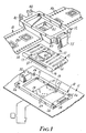
- the test socket of the present invention consists of a frame member having a base 10 adapted for alignment on a printed circuit board 11.
- a cover plate 12 is hinged to the base 10.
- a flexible circuit member comprising a strip of beam tape 15 is folded about an elastomeric pad 16 and a locating brace 37.
- the brace 37 is provided with alignment means in the form of pins 17 supported to position and register both the beam tape 15 and a strip of flexible tape 18, the tape 18 supports, in spaced relation therealong, a series of high performance integrated circuit devices or chips 20.
- Alignment between the connector portions of the beam tape 15 and contacts 29 on the printed circuit board is also provided by the pins 17 and maintained by fasteners, such as bolts 26 to locate the connector portions 63 of the beam tape 15 with the contacts 29 on the printed circuit board 11 and to urge the contact points on the beam tape into electrical contact with the contacts on the printed circuit board.
- the base 10 is generally rectangular in shape and is formed with a centrally located rectangular opening 31. At one end is a pillar 32 which serves as a hinge support for the cover 12. Opposite the pillar 32 is a projection 34 which cooperates with a spring biased latch member 35 supported on the cover 12 and pivoted thereto but biased by a torsion spring into latching engagement with the projection 34 such that the projection 34 will engage a recess 36 which extends transversely of the latch member 35 as shown in Figures 1 and 4.
- the base has a locating brace 37 which extends across the opening 31 and is joined to the side members of the base forming the opening 31. The brace 37 supports the pins 17 and the resilient material 16 supporting the beam tape 15.
- the cover 12 is pivoted on the pillar 32 by means of a pin 40 extending through legs 41 and 42 projecting parallelly from one end of the cover.
- the cover 12 is hinged by the pin 40 to move from an open position to a closed position mat:ing closely with the base to urge the beam tape and the contacts of a chip, whether on tape or on a carrier, into contact with each other.
- Positioned generally centrally of the cover 12 is an opening 45 to avoid pressure directly to a chip.
- Registration is made between a beam tape of 15 and the contact portions of the tape 18 as the cover is closed. This alignment and registration is afforded by alignment or positioning means such as the square pins 17 which are provided on the base 10 and fit in the edge sprocket holes 50 of the tape 18.
- a chip carrier may be registered on the pins 17 to locate a chip on the beam tape 15.
- the tape 18 is formed according to U.S. patent No. 3,832,769, issued September 3, 1974 and incorporated by reference.
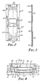
- the beam tape 15, as illustrated in Figures 1, 2, and 3 comprises a contact portion and a connector portion.
- the contact portion 47 of the tape 15 is generally centrally located with respect to the illustrated strip and comprises a plurality of contacts 60 which form in the illustrated embodiment a generally rectangular outline with a plurality of the contacts 60 in each of four rows thereof about the center of the strip.
- These contact portions 60 are joined by conductive material in holes through the tape to circuit traces 61 which electrically conductively join the contacts 60 to connector pads 63 in the connector portion of the tape strip.
- the connector pads 63 are similarly formed by conductive columns which extend through the backing and connect to the conductive circuit traces 61.
- Tape 15 is a polyamide film backing having a conductive metal coating on one surface. Then by etching or masking processes the contact areas and circuit traces are formed on the surface of the tape.
- a preferred backing for the tape 15 is KaptonTM polyamide "H" film available from Du Pont of Wilmington, Delaware, U.S.A.
- the contacts 60 in the contact portion of the tape are slightly embossed from the surface of the tape to provide a hump in the tape at the area of the contact. This humped contact at one end of each circuit trace provides the tape contact and may have a further metal coating on the surface thereof.
- the tape 15 When the tape 15 is formed it is wrapped around an elastomeric support pad 16, e.g. a silicone rubber pad as shown in Figure 1, positioned about the brace 37 which, as shown for illustration is out of the opening 31 across which it is positioned.
- the compliant nature of the pad 16 provides a support for the tape material 15 such that contact is maintained between the contacts 60 and the contact points of the chip 20 or a single chip which may be unsupported by the tape and positioned in a plate set on the pins 17 having an aperture to receive the chip such that the cover 12, when closed will maintain contact between said chip and the opposed crowns.
- chips to be tested afford 1 to 1 > x ⁇ ⁇ contact points 60 about the center of the contact portion of the tape 15 to which then are connected to 1 to 1 > x ⁇ ⁇ connector points for connection to the printed circuit board.
- the pins 17 align the contact points with the base 10 and align the connector pads with the base.
- the pins 17 on the brace 37 fit into holes 19 formed in the printed circuit board 11 outside the area of the contacts 29 to then align the tape 15 and connector pads to the contacts 29.
- the abutting ends of the tape 15 and the connector pads and the contacts 29 can be maintained in position by the use of a conductive adhesive tape 25 positioned against the exposed connector pads 63.
- the tape 25 is a layer of pressure sensitive adhesive which is formed to be conductive by conductive particles being disposed in the layer of adhesive as disclosed in U.S. patent No. 4,606,962, issued August 19, 1986, and incorporated herein by reference.
- This adhesive tape is conductive only in a path between the opposite surfaces and thus this tape will join the connectors 63 to the contacts on the printed circuit board 11.
- An example of such conductive tape is C 3100X and C 4100X available from Minnesota Mining and Manufacturing Company of St. Paul, Minnesota, U.S.A. Alignment, as above noted, is established by the alignment or locating pins 17 fitting in the printed circuit board and holes 65 and 66 in the tape 15.
- Alignment of the chips is maintained through the pins 17, and when the cover 12 is opened, the chip is advanced by moving the tape 18 forward to register openings 50 along the marginal edges on pins 17 to locate a second chip aligned with the contacts of the beam tape 15. The cover is then swung to the closed position and the latch plate 35 engages the projection 34. There is compression on the pad 16 amounting to 17 to 29 grams per contact in the illustrated socket. The registration is thus established and the chip is located in the opening.
- the tape 15 is registered by the pins 17 passing through the holes 65 and 66, and contact is made with the printed circuit board contacts through the tape 25 on the Z-axis and compressed pad 16 under the force of the fasteners 26, or solely through the compressive contact between the pads 63 and the contacts 29.
Abstract
Description
- This invention relates to an improvement in devices for electrically testing high performance integrated circuit devices or chips, and in one aspect to an improved test socket for supporting the chip, whether on tape or not, free of detrimental effect on the device or tape and affording rapid facile positive electrical connection with the contact points of said device.
- As the development of integrated circuit devices continues, i.e. "chips", to provide in a single chip more and more capability, they result in more, and more, and more closely spaced contact points for electrically connecting circuits to a chip. It is always a step in the manufacture to test the chips. Performance of a chip is tested by placing each chip in a test fixture or test socket and connecting all of the contact points electrically to the test fixture such that a series of tests may be run on each of the modes of operation to determine the quality of the chip. As the contact points become located closer and closer together it has become increasingly difficult to design a test socket which has hard wired contacts close enough together to assure contact with the individual contact points of the chip, and such test sockets are not suitable for testing integrated circuit devices packaged on a tape. Examples of such test sockets are present in U.S.A. patents Nos. 3,551,878; 3,914,007; 4,130,327; 4,508,403; 4,541,676; and application Serial No. 643,237, filed August 22, 1984, and assigned to the assignee of this application. Thus, with the development of technologies for chip-on-tape manufacture it was necessary to also be able to test the chips on the tape requiring registration with and surface contact to each of the contact points of such chips. To do this requires high density terminals in the test socket which were not easily afforded by the mechanical fixturing of the test sockets. The requirements for chip-on-tape testing of chips having high density contact points required the carrier tape handling capability, a hot test capability, an intelligent operator interface, quick load and unload of tape and flexibility as to the set up for different chip-on-tape formats.
- The present invention provides a manual tape test station having strip or tape handling capability or individual chip handling capability, hot test capability, an intelligent operator interface which provides for the location of the chip, quick load and unload of the chip and adapted for change from one chip format to another.
- The present invention provides a temporary electronic circuit socket connector which can be utilized to effectively connect integrated circuit devices or chips, which are carried on a tape during manufacture, to a circuit and which may be for the purpose of testing the device or chip. The connector is suitable as a test fixture for chips and comprises a single metal layer beam tape which has been etched to define contact area portions and connector area portions joined by circuit traces.
- Preferably contact pads are formed on one surface of a dielectric backing, and conductive columns extend therethrough to circuit traces formed from a conductive metal coating on the opposite surface. The pads are crowns formed in the contact area to insure good contact to the contact points of the chip. The contact pads in the contact portion of the beam tape are connected by the circuit traces to the connector pads in the connector portion. The beam tape is bent to dispose the contact portion and the connector portions in vertically spaced relation with each of the same being outwardly exposed and the circuit traces being positioned inwardly. A compliant elastomer pad is disposed about a locating brace in a frame member and between the contact portion and the connector portion. The frame member which is adapted to be precisely located on the surface of a circuit board forming the test device or at least a portion thereof. The frame member is then fixed to the circuit board by suitable fastening elements. Alignment means on the frame member afford registration of the frame member with the printed circuit board and with the beam tape whereby the connector pads of the tape are properly aligned with pads on the circuit board and sections of the tape carrying the chip are properly aligned over the contact portions of the beam tape. A cover member supported on the frame affords means for temporarily pressing the chip-on-tape segment or chip against the contact portion of the beam tape against the resilience of the elastomer pad. This pressure member may be latched in place for continuous contact by a readily releasable latch means. The pad between the locating brace and the printed circuit board presses the connector pads against contacts on the printed circuit board to maintain contact during the burn-in and\or testing. Thus the socket, beam tape and elastomer pad may be readily changed for testing other chip formats utilizing the same printed circuit board.
- Alternatively, the connector portion of the beam tape is adhered in registration with the contacts of a printed circuit board by the use of a double sided pressure-sensitive adhesive coated electrically conductive tape which is conductive only transversely through the tape and affords the electrical connection between the connector pads on the beam tape and the opposed contacts on the printed circuit board. The frame member is also fastened to the printed circuit board to maintain it stable for chip changes. Separate housings, registrable with the printed circuit board, may be used with other beam tapes, but the adhesive should be removed as the sockets are changed.
- The present invention will be further described with reference to the accompanying drawing wherein:
- Figure 1 is an exploded view of the chip test socket formed according to the present invention;
- Figure 2 is a plan view of a strip of the beam tape;
- Figure 3 is a schematic sectional view of the beam tape:
- Figure 4 is a side view of the chip test socket;
and - Figure 5 is an enlarged illustrative sectional view showing the relationship of the printed circuit board and the connecting beam tape.
- Referring to Figure 1, the test socket of the present invention consists of a frame member having a
base 10 adapted for alignment on a printedcircuit board 11. Acover plate 12 is hinged to thebase 10. A flexible circuit member comprising a strip ofbeam tape 15 is folded about anelastomeric pad 16 and a locatingbrace 37. Thebrace 37 is provided with alignment means in the form ofpins 17 supported to position and register both thebeam tape 15 and a strip offlexible tape 18, thetape 18 supports, in spaced relation therealong, a series of high performance integrated circuit devices or chips 20. Alignment between the connector portions of thebeam tape 15 andcontacts 29 on the printed circuit board is also provided by thepins 17 and maintained by fasteners, such asbolts 26 to locate theconnector portions 63 of thebeam tape 15 with thecontacts 29 on the printedcircuit board 11 and to urge the contact points on the beam tape into electrical contact with the contacts on the printed circuit board. - The
base 10 is generally rectangular in shape and is formed with a centrally locatedrectangular opening 31. At one end is apillar 32 which serves as a hinge support for thecover 12. Opposite thepillar 32 is aprojection 34 which cooperates with a springbiased latch member 35 supported on thecover 12 and pivoted thereto but biased by a torsion spring into latching engagement with theprojection 34 such that theprojection 34 will engage arecess 36 which extends transversely of thelatch member 35 as shown in Figures 1 and 4. The base has a locatingbrace 37 which extends across the opening 31 and is joined to the side members of the base forming the opening 31. Thebrace 37 supports thepins 17 and theresilient material 16 supporting thebeam tape 15. - The
cover 12, as mentioned, is pivoted on thepillar 32 by means of apin 40 extending throughlegs cover 12 is hinged by thepin 40 to move from an open position to a closed position mat:ing closely with the base to urge the beam tape and the contacts of a chip, whether on tape or on a carrier, into contact with each other. Positioned generally centrally of thecover 12 is anopening 45 to avoid pressure directly to a chip. Registration is made between a beam tape of 15 and the contact portions of thetape 18 as the cover is closed. This alignment and registration is afforded by alignment or positioning means such as thesquare pins 17 which are provided on thebase 10 and fit in theedge sprocket holes 50 of thetape 18. Alternatively, a chip carrier may be registered on thepins 17 to locate a chip on thebeam tape 15. Thetape 18 is formed according to U.S. patent No. 3,832,769, issued September 3, 1974 and incorporated by reference. - The
beam tape 15, as illustrated in Figures 1, 2, and 3 comprises a contact portion and a connector portion. As illustrated in Figures 2 and 3, thecontact portion 47 of thetape 15 is generally centrally located with respect to the illustrated strip and comprises a plurality ofcontacts 60 which form in the illustrated embodiment a generally rectangular outline with a plurality of thecontacts 60 in each of four rows thereof about the center of the strip. Thesecontact portions 60 are joined by conductive material in holes through the tape tocircuit traces 61 which electrically conductively join thecontacts 60 toconnector pads 63 in the connector portion of the tape strip. Theconnector pads 63 are similarly formed by conductive columns which extend through the backing and connect to theconductive circuit traces 61. Alignment of the connector portion andpads 63 with the contacts in the printedcircuit board 11 is afforded byalignment pins 17 which pass throughregistration holes 65 positioned adjacent to the contact area of thetape 15 andregistration holes 66 positioned through the tape adjacent the connector area of the tape.Tape 15 is a polyamide film backing having a conductive metal coating on one surface. Then by etching or masking processes the contact areas and circuit traces are formed on the surface of the tape. A preferred backing for thetape 15 is Kapton™ polyamide "H" film available from Du Pont of Wilmington, Delaware, U.S.A. As indicated in Figures 3 and 4, thecontacts 60 in the contact portion of the tape are slightly embossed from the surface of the tape to provide a hump in the tape at the area of the contact. This humped contact at one end of each circuit trace provides the tape contact and may have a further metal coating on the surface thereof. - When the
tape 15 is formed it is wrapped around anelastomeric support pad 16, e.g. a silicone rubber pad as shown in Figure 1, positioned about thebrace 37 which, as shown for illustration is out of theopening 31 across which it is positioned. The compliant nature of thepad 16 provides a support for thetape material 15 such that contact is maintained between thecontacts 60 and the contact points of the chip 20 or a single chip which may be unsupported by the tape and positioned in a plate set on thepins 17 having an aperture to receive the chip such that thecover 12, when closed will maintain contact between said chip and the opposed crowns. - In this test socket there are no formed or stamped metal contacts or pins between the printed circuit board and the contact points of the chip. The photographically patterned contact areas, circuit traces and connector areas of the
beam tape 15 form the circuit path from the chip to the circuit board of the test equipment. Theelastomeric pad 16 provides the continued energy necessary to maintain reliable connections with all of the contact points. It is maintained under compression with the printed circuit board by thefasteners 26. When thecover 12 is latched in the mating position against the base 10 contact is maintained between the chip andcontact pads 60 by thepad 16 for reliable connection during the test cycles. - Typically chips to be tested afford 1 to 1 > x < ∞ contact points 60 about the center of the contact portion of the
tape 15 to which then are connected to 1 to 1 > x < ∞ connector points for connection to the printed circuit board. When the connector end portions of the tape, as illustrated in Figure 2, are folded about opposed ends of thepad 16, as illustrated in Figures 4 and 5, thepins 17 align the contact points with thebase 10 and align the connector pads with the base. Thepins 17 on thebrace 37 fit intoholes 19 formed in the printedcircuit board 11 outside the area of thecontacts 29 to then align thetape 15 and connector pads to thecontacts 29. The abutting ends of thetape 15 and the connector pads and thecontacts 29 can be maintained in position by the use of a conductive adhesive tape 25 positioned against the exposedconnector pads 63. The tape 25 is a layer of pressure sensitive adhesive which is formed to be conductive by conductive particles being disposed in the layer of adhesive as disclosed in U.S. patent No. 4,606,962, issued August 19, 1986, and incorporated herein by reference. This adhesive tape is conductive only in a path between the opposite surfaces and thus this tape will join theconnectors 63 to the contacts on the printedcircuit board 11. An example of such conductive tape is C 3100X and C 4100X available from Minnesota Mining and Manufacturing Company of St. Paul, Minnesota, U.S.A. Alignment, as above noted, is established by the alignment or locatingpins 17 fitting in the printed circuit board and holes 65 and 66 in thetape 15. - Alignment of the chips is maintained through the
pins 17, and when thecover 12 is opened, the chip is advanced by moving thetape 18 forward to registeropenings 50 along the marginal edges onpins 17 to locate a second chip aligned with the contacts of thebeam tape 15. The cover is then swung to the closed position and thelatch plate 35 engages theprojection 34. There is compression on thepad 16 amounting to 17 to 29 grams per contact in the illustrated socket. The registration is thus established and the chip is located in the opening. Thetape 15 is registered by thepins 17 passing through theholes compressed pad 16 under the force of thefasteners 26, or solely through the compressive contact between thepads 63 and thecontacts 29. - This system affords reliability in testing, permits the circuit to be changed readily to match different formats for the chips, and the selections of tape permit testing over a wide range of elevated temperatures. Having thus described the present invention with respect to a preferred embodiment it will be appreciated that changes may be incorporated without departing from the scope of this invention as described in the attached claims.
Claims (10)
a conductive metal layer beam tape, one portion of said beam tape defining a contact area having contact portions to contact the contact points of the integrated circuit device and a connector area having spaced connector portions for connection to correspondingly spaced contacts on a circuit board, said beam tape being folded between said contact area and said connector area, a compliant elastomeric pad disposed between said contact area and said connector area for supporting said contact area and said connector area, that said frame includes means for locating said connector area with respect to the contacts of a printed circuit board and means for locating the contact points on an integrated circuit device with respect to said contact area, and that
means are provided for pressing an integrated circuit device onto said contact area against the resilient support of said elastomeric pad.
characterized in that a strip of tape having opposite surfaces, which is conductive through the tape between said opposite surfaces, is applied over the connector area of said beam tape.
characterized in that said beam tape comprises a thin dielectric backing and on one surface a pattern of conductive strips defining circuit traces which strips are joined to individual crowns on the opposite surface of the tape defining said contact portions and connector portions.
characterized in that said frame comprises a plate having a rectangular opening and a brace spanning said opening, said elastomeric pad being positioned about said brace to urge said connector area toward a said circuit board and said contact area toward a said integrated circuit device.
characterized in that said brace has pin means extending from opposite surfaces thereof and through said beam tape adjacent to said contact area and said connector area for registering said beam tape to said frame.
characterized in that fastening means secure said frame to a said circuit board with the elastomeric pad pressing said tape connector area toward said circuit board.
characterized in that said pin means includes means for registering said frame with a said circuit board for registering said connector area with a series of contacts formed on said circuit board.
characterized in that said means for pressing said integrated circuit device onto said contact area comprises a cover hinged to said frame and said cover is formed to move from an open position to a closed mating position with said frame to urge said beam tape contact area against said elastomeric pad for urging a said integrated circuit device into intimate electrical contact therewith, and releasable latch means for holding said cover in said mating position.
characterized in that registration means afford alignment of a said integrated circuit device with said contact area of said beam tape for making said electrical contact therewith.
characterized in that said registration means comprises a brace positioned on said frame, that said elastomeric pad is positioned about said brace to urge said connector area toward a said circuit board, and that said registration means comprises pins means extending from said brace, through said pad and said beam tape, for engagement with a said integrated circuit device.
Applications Claiming Priority (4)
| Application Number | Priority Date | Filing Date | Title |
|---|---|---|---|
| US10120387A | 1987-09-25 | 1987-09-25 | |
| US101203 | 1987-09-25 | ||
| US07/217,212 US4859189A (en) | 1987-09-25 | 1988-07-08 | Multipurpose socket |
| US217212 | 1988-07-08 |
Publications (3)
| Publication Number | Publication Date |
|---|---|
| EP0310302A2 true EP0310302A2 (en) | 1989-04-05 |
| EP0310302A3 EP0310302A3 (en) | 1990-10-17 |
| EP0310302B1 EP0310302B1 (en) | 1994-10-26 |
Family
ID=26798010
Family Applications (1)
| Application Number | Title | Priority Date | Filing Date |
|---|---|---|---|
| EP88308813A Expired - Lifetime EP0310302B1 (en) | 1987-09-25 | 1988-09-22 | Multipurpose socket |
Country Status (6)
| Country | Link |
|---|---|
| US (1) | US4859189A (en) |
| EP (1) | EP0310302B1 (en) |
| JP (1) | JPH01121776A (en) |
| KR (1) | KR970003521B1 (en) |
| DE (1) | DE3851932T2 (en) |
| MY (1) | MY103606A (en) |
Cited By (11)
| Publication number | Priority date | Publication date | Assignee | Title |
|---|---|---|---|---|
| US4969828A (en) * | 1989-05-17 | 1990-11-13 | Amp Incorporated | Electrical socket for TAB IC's |
| GB2275365A (en) * | 1992-12-10 | 1994-08-24 | Yamaichi Electronics Co Ltd | Socket for IC carrier |
| GB2276988A (en) * | 1993-04-09 | 1994-10-12 | Minnesota Mining & Mfg | I.C.test and burn-in socket |
| WO2000011920A1 (en) * | 1998-08-18 | 2000-03-02 | Infineon Technologies Ag | Printed circuit plate used for testing electric components |
| WO2001009980A2 (en) * | 1999-08-02 | 2001-02-08 | Gryphics, Inc. | Controlled compliance fine pitch interconnect |
| US6409521B1 (en) | 1997-05-06 | 2002-06-25 | Gryphics, Inc. | Multi-mode compliant connector and replaceable chip module utilizing the same |
| US6572396B1 (en) | 1999-02-02 | 2003-06-03 | Gryphics, Inc. | Low or zero insertion force connector for printed circuit boards and electrical devices |
| US6830460B1 (en) | 1999-08-02 | 2004-12-14 | Gryphics, Inc. | Controlled compliance fine pitch interconnect |
| EP1876454A1 (en) * | 2006-07-07 | 2008-01-09 | Siemens Aktiengesellschaft | Method for testing chips electrically |
| US7900347B2 (en) | 2000-01-20 | 2011-03-08 | Cascade Microtech, Inc. | Method of making a compliant interconnect assembly |
| EP2040518A3 (en) * | 2007-09-18 | 2012-03-28 | Japan Aviation Electronics Industry, Limited | Heat transfer member and connector |
Families Citing this family (35)
| Publication number | Priority date | Publication date | Assignee | Title |
|---|---|---|---|---|
| DE3927752A1 (en) * | 1989-08-23 | 1991-02-28 | Stocko Metallwarenfab Henkels | DISPLAY CONTACT WITH A PCB |
| US5123850A (en) * | 1990-04-06 | 1992-06-23 | Texas Instruments Incorporated | Non-destructive burn-in test socket for integrated circuit die |
| US5373230A (en) * | 1991-06-17 | 1994-12-13 | Itt Corporation | Test clip for five pitch IC |
| JPH06510122A (en) * | 1991-08-23 | 1994-11-10 | エヌチップ インコーポレイテッド | Burn-in techniques for unpackaged integrated circuits |
| US5131852A (en) * | 1991-08-23 | 1992-07-21 | Amp Incorporated | Electrical socket |
| US5541524A (en) * | 1991-08-23 | 1996-07-30 | Nchip, Inc. | Burn-in technologies for unpackaged integrated circuits |
| US5161984A (en) * | 1991-10-16 | 1992-11-10 | Amp Incorporated | Electrical socket |
| US5278724A (en) * | 1992-07-06 | 1994-01-11 | International Business Machines Corporation | Electronic package and method of making same |
| US5854534A (en) * | 1992-08-05 | 1998-12-29 | Fujitsu Limited | Controlled impedence interposer substrate |
| US5402077A (en) * | 1992-11-20 | 1995-03-28 | Micromodule Systems, Inc. | Bare die carrier |
| US6937044B1 (en) | 1992-11-20 | 2005-08-30 | Kulicke & Soffa Industries, Inc. | Bare die carrier |
| US5517125A (en) * | 1993-07-09 | 1996-05-14 | Aehr Test Systems, Inc. | Reusable die carrier for burn-in and burn-in process |
| US5456404A (en) * | 1993-10-28 | 1995-10-10 | Digital Equipment Corporation | Method of testing semiconductor chips with reusable test package |
| US5508228A (en) * | 1994-02-14 | 1996-04-16 | Microelectronics And Computer Technology Corporation | Compliant electrically connective bumps for an adhesive flip chip integrated circuit device and methods for forming same |
| US5498970A (en) * | 1995-02-06 | 1996-03-12 | Minnesota Mining And Manufacturing | Top load socket for ball grid array devices |
| DE69611302T2 (en) * | 1995-07-07 | 2001-08-09 | Minnesota Mining & Mfg | ASSEMBLING A DISCONNECTABLE ELECTRICAL CONNECTOR WITH A MATRIX-LEADING PROTECTION |
| US5772467A (en) * | 1996-06-04 | 1998-06-30 | Alcoa Fujikura Ltd. | Terminal free connector and method |
| US5917709A (en) * | 1997-06-16 | 1999-06-29 | Eastman Kodak Company | Multiple circuit board assembly having an interconnect mechanism that includes a flex connector |
| KR100446112B1 (en) * | 1997-08-14 | 2004-10-14 | 삼성전자주식회사 | Combination 16/32 para and track, and a socket guide, specially concerned with remarkably reducing a replacing work time by replacing a test board only in a test unit even though the size of a semiconductor chip package is changed during a test |
| US5945203A (en) * | 1997-10-14 | 1999-08-31 | Zms Llc | Stratified composite dielectric and method of fabrication |
| TW442554B (en) * | 1999-04-05 | 2001-06-23 | Four Pillars Entpr Co Ltd | Multi-functional electrically and thermally conductive adhesive tape |
| US6396698B1 (en) * | 2001-01-18 | 2002-05-28 | Agilent Technologies, Inc. | Retention module adapter |
| WO2002080268A1 (en) * | 2001-03-30 | 2002-10-10 | Infineon Technologies Ag | A substrate for mounting a semiconductor chip |
| US20040144945A1 (en) * | 2001-05-14 | 2004-07-29 | Luciano Bonomi | Valve with metal seal between the coupled parts of its body |
| US6835071B2 (en) * | 2001-07-18 | 2004-12-28 | Tyco Electronics Corporation | Elastomeric connector interconnecting flexible circuits and circuit board and method of manufacturing the same |
| EP1642364A1 (en) | 2003-07-07 | 2006-04-05 | Gryphics, Inc. | Normally closed zero insertion force connector |
| JP4316483B2 (en) * | 2004-12-08 | 2009-08-19 | ユーアイ電子株式会社 | Printed circuit board manufacturing method and printed circuit board |
| JP4179620B2 (en) * | 2005-04-28 | 2008-11-12 | 日本航空電子工業株式会社 | connector |
| JP4188942B2 (en) * | 2005-05-12 | 2008-12-03 | 日本航空電子工業株式会社 | connector |
| US7752746B2 (en) * | 2007-08-28 | 2010-07-13 | Unitech Printed Circuit Board Corp. | Method of partially attaching an additional attaching material for various types of printed circuit boards |
| TWM332194U (en) * | 2007-12-04 | 2008-05-11 | Princeton Technology Corp | Testing circuit board |
| JP4763838B2 (en) * | 2009-07-29 | 2011-08-31 | 日本航空電子工業株式会社 | connector |
| KR101030804B1 (en) * | 2010-04-09 | 2011-04-27 | 이승룡 | Interface, method for fabricating the same interface, test socket comprising the same interface, and test apparatus comprising the test socket |
| JP5090502B2 (en) * | 2010-06-30 | 2012-12-05 | 日本航空電子工業株式会社 | Connector assembly |
| US11171440B2 (en) * | 2019-03-20 | 2021-11-09 | Aptiv Technologies Limited | Backing plate for mounting and sealing an electrical connector to an intermediate surface |
Citations (4)
| Publication number | Priority date | Publication date | Assignee | Title |
|---|---|---|---|---|
| GB2164213A (en) * | 1984-09-06 | 1986-03-12 | Nec Corp | Structure for connecting leadless chip carrier to surface contacts |
| GB2169154A (en) * | 1984-12-31 | 1986-07-02 | Gen Electric | Pressure-fit electrical socket for direct interconnection to a semiconductor chip |
| US4655524A (en) * | 1985-01-07 | 1987-04-07 | Rogers Corporation | Solderless connection apparatus |
| WO1988005544A1 (en) * | 1987-01-20 | 1988-07-28 | Hughes Aircraft Company | Test connector for electrical devices |
Family Cites Families (11)
| Publication number | Priority date | Publication date | Assignee | Title |
|---|---|---|---|---|
| US3832769A (en) * | 1971-05-26 | 1974-09-03 | Minnesota Mining & Mfg | Circuitry and method |
| US3868724A (en) * | 1973-11-21 | 1975-02-25 | Fairchild Camera Instr Co | Multi-layer connecting structures for packaging semiconductor devices mounted on a flexible carrier |
| US4012117A (en) * | 1974-07-29 | 1977-03-15 | Rca Corporation | Liquid crystal module |
| NL7610306A (en) * | 1976-09-16 | 1978-03-20 | Du Pont | CONTACT DEVICE FOR AN INTEGRATED CIRCUIT. |
| US4130327A (en) * | 1977-05-27 | 1978-12-19 | Bunker Ramo Corporation | Electrical connector having a resilient cover |
| US4506938A (en) * | 1982-07-06 | 1985-03-26 | At&T Bell Laboratories | Integrated circuit chip carrier mounting arrangement |
| US4597617A (en) * | 1984-03-19 | 1986-07-01 | Tektronix, Inc. | Pressure interconnect package for integrated circuits |
| US4548862A (en) * | 1984-09-04 | 1985-10-22 | Minnesota Mining And Manufacturing Company | Flexible tape having bridges of electrically conductive particles extending across its pressure-sensitive adhesive layer |
| US4621884A (en) * | 1984-12-19 | 1986-11-11 | Amp Incorporated | Electrical socket having a hinged cover |
| US4601525A (en) * | 1985-05-20 | 1986-07-22 | Amp Incorporated | Cover for chip carrier sockets |
| US4658331A (en) * | 1985-09-09 | 1987-04-14 | Tektronix, Inc. | Mounting an integrated circuit chip to an etched circuit board |
-
1988
- 1988-07-08 US US07/217,212 patent/US4859189A/en not_active Expired - Lifetime
- 1988-09-10 MY MYPI88001011A patent/MY103606A/en unknown
- 1988-09-22 JP JP63238643A patent/JPH01121776A/en active Pending
- 1988-09-22 EP EP88308813A patent/EP0310302B1/en not_active Expired - Lifetime
- 1988-09-22 DE DE3851932T patent/DE3851932T2/en not_active Expired - Fee Related
- 1988-09-23 KR KR1019880012346A patent/KR970003521B1/en not_active IP Right Cessation
Patent Citations (4)
| Publication number | Priority date | Publication date | Assignee | Title |
|---|---|---|---|---|
| GB2164213A (en) * | 1984-09-06 | 1986-03-12 | Nec Corp | Structure for connecting leadless chip carrier to surface contacts |
| GB2169154A (en) * | 1984-12-31 | 1986-07-02 | Gen Electric | Pressure-fit electrical socket for direct interconnection to a semiconductor chip |
| US4655524A (en) * | 1985-01-07 | 1987-04-07 | Rogers Corporation | Solderless connection apparatus |
| WO1988005544A1 (en) * | 1987-01-20 | 1988-07-28 | Hughes Aircraft Company | Test connector for electrical devices |
Cited By (16)
| Publication number | Priority date | Publication date | Assignee | Title |
|---|---|---|---|---|
| EP0398506A2 (en) * | 1989-05-17 | 1990-11-22 | The Whitaker Corporation | Electrical socket for tab IC's |
| EP0398506A3 (en) * | 1989-05-17 | 1991-06-26 | The Whitaker Corporation | Electrical socket for tab ic's |
| US4969828A (en) * | 1989-05-17 | 1990-11-13 | Amp Incorporated | Electrical socket for TAB IC's |
| GB2275365A (en) * | 1992-12-10 | 1994-08-24 | Yamaichi Electronics Co Ltd | Socket for IC carrier |
| GB2275365B (en) * | 1992-12-10 | 1996-10-16 | Yamaichi Electronics Co Ltd | Socket for IC carrier |
| GB2276988A (en) * | 1993-04-09 | 1994-10-12 | Minnesota Mining & Mfg | I.C.test and burn-in socket |
| GB2276988B (en) * | 1993-04-09 | 1996-10-02 | Minnesota Mining & Mfg | Top load socket and carrier |
| US6409521B1 (en) | 1997-05-06 | 2002-06-25 | Gryphics, Inc. | Multi-mode compliant connector and replaceable chip module utilizing the same |
| WO2000011920A1 (en) * | 1998-08-18 | 2000-03-02 | Infineon Technologies Ag | Printed circuit plate used for testing electric components |
| US6572396B1 (en) | 1999-02-02 | 2003-06-03 | Gryphics, Inc. | Low or zero insertion force connector for printed circuit boards and electrical devices |
| WO2001009980A2 (en) * | 1999-08-02 | 2001-02-08 | Gryphics, Inc. | Controlled compliance fine pitch interconnect |
| WO2001009980A3 (en) * | 1999-08-02 | 2001-08-30 | Gryphics Inc | Controlled compliance fine pitch interconnect |
| US6830460B1 (en) | 1999-08-02 | 2004-12-14 | Gryphics, Inc. | Controlled compliance fine pitch interconnect |
| US7900347B2 (en) | 2000-01-20 | 2011-03-08 | Cascade Microtech, Inc. | Method of making a compliant interconnect assembly |
| EP1876454A1 (en) * | 2006-07-07 | 2008-01-09 | Siemens Aktiengesellschaft | Method for testing chips electrically |
| EP2040518A3 (en) * | 2007-09-18 | 2012-03-28 | Japan Aviation Electronics Industry, Limited | Heat transfer member and connector |
Also Published As
| Publication number | Publication date |
|---|---|
| KR970003521B1 (en) | 1997-03-18 |
| MY103606A (en) | 1993-08-28 |
| JPH01121776A (en) | 1989-05-15 |
| EP0310302A3 (en) | 1990-10-17 |
| DE3851932T2 (en) | 1995-05-24 |
| DE3851932D1 (en) | 1994-12-01 |
| EP0310302B1 (en) | 1994-10-26 |
| US4859189A (en) | 1989-08-22 |
| KR890005523A (en) | 1989-05-15 |
Similar Documents
| Publication | Publication Date | Title |
|---|---|---|
| US4859189A (en) | Multipurpose socket | |
| JP3280796B2 (en) | IC device equipment | |
| US4340860A (en) | Integrated circuit carrier package test probe | |
| EP0398506B1 (en) | Electrical socket for tab IC's | |
| US6782614B2 (en) | Contact pin assembly, contact pin assembly manufacturing method, contact pin assembling structure, contact pin assembling structure manufacturing method, and socket for electrical parts | |
| US5530376A (en) | Reusable carrier for burn-in/testing of non packaged die | |
| KR100385014B1 (en) | Burn-in reusable die carriers and burn-in method | |
| US5440240A (en) | Z-axis interconnect for discrete die burn-in for nonpackaged die | |
| US6091251A (en) | Discrete die burn-in for nonpackaged die | |
| US5705933A (en) | Resuable carrier for burn-in/testing on non packaged die | |
| US5543725A (en) | Reusable carrier for burn-in/testing on non packaged die | |
| EP1691206A2 (en) | Method and apparatus for testing semiconductor dice | |
| JPH01502451A (en) | Test connectors for electrical equipment | |
| US5161984A (en) | Electrical socket | |
| JPH04230866A (en) | Ic adaptor | |
| US5977784A (en) | Method of performing an operation on an integrated circuit | |
| US5202622A (en) | Adapter and test fixture for an integrated circuit device package | |
| US4943768A (en) | Testing device for electrical circuit boards | |
| US5177436A (en) | Contactor for testing integrated circuit chips mounted in molded carrier rings | |
| JP3051596B2 (en) | Semiconductor chip test socket | |
| CA1289681C (en) | Multipurpose socket | |
| JPH09275168A (en) | Testing ic socket and flexible circuit board usable for the ic socket | |
| US4887030A (en) | Testing device for electrical circuit boards | |
| US4950981A (en) | Apparatus for testing a circuit board | |
| US5738528A (en) | IC carrier |
Legal Events
| Date | Code | Title | Description |
|---|---|---|---|
| PUAI | Public reference made under article 153(3) epc to a published international application that has entered the european phase |
Free format text: ORIGINAL CODE: 0009012 |
|
| AK | Designated contracting states |
Kind code of ref document: A2 Designated state(s): DE FR GB IT NL |
|
| PUAL | Search report despatched |
Free format text: ORIGINAL CODE: 0009013 |
|
| RHK1 | Main classification (correction) |
Ipc: H05K 7/10 |
|
| AK | Designated contracting states |
Kind code of ref document: A3 Designated state(s): DE FR GB IT NL |
|
| 17P | Request for examination filed |
Effective date: 19910102 |
|
| 17Q | First examination report despatched |
Effective date: 19921012 |
|
| GRAA | (expected) grant |
Free format text: ORIGINAL CODE: 0009210 |
|
| ITF | It: translation for a ep patent filed |
Owner name: BARZANO' E ZANARDO ROMA S.P.A. |
|
| AK | Designated contracting states |
Kind code of ref document: B1 Designated state(s): DE FR GB IT NL |
|
| REF | Corresponds to: |
Ref document number: 3851932 Country of ref document: DE Date of ref document: 19941201 |
|
| ET | Fr: translation filed | ||
| PLBE | No opposition filed within time limit |
Free format text: ORIGINAL CODE: 0009261 |
|
| STAA | Information on the status of an ep patent application or granted ep patent |
Free format text: STATUS: NO OPPOSITION FILED WITHIN TIME LIMIT |
|
| 26N | No opposition filed | ||
| K2C3 | Correction of patent specification (complete document) published |
Effective date: 19941026 |
|
| PGFP | Annual fee paid to national office [announced via postgrant information from national office to epo] |
Ref country code: FR Payment date: 19970820 Year of fee payment: 10 |
|
| PGFP | Annual fee paid to national office [announced via postgrant information from national office to epo] |
Ref country code: NL Payment date: 19970821 Year of fee payment: 10 |
|
| PGFP | Annual fee paid to national office [announced via postgrant information from national office to epo] |
Ref country code: DE Payment date: 19970822 Year of fee payment: 10 |
|
| PGFP | Annual fee paid to national office [announced via postgrant information from national office to epo] |
Ref country code: GB Payment date: 19970826 Year of fee payment: 10 |
|
| PG25 | Lapsed in a contracting state [announced via postgrant information from national office to epo] |
Ref country code: GB Free format text: LAPSE BECAUSE OF NON-PAYMENT OF DUE FEES Effective date: 19980922 |
|
| PG25 | Lapsed in a contracting state [announced via postgrant information from national office to epo] |
Ref country code: NL Free format text: LAPSE BECAUSE OF NON-PAYMENT OF DUE FEES Effective date: 19990401 |
|
| GBPC | Gb: european patent ceased through non-payment of renewal fee |
Effective date: 19980922 |
|
| PG25 | Lapsed in a contracting state [announced via postgrant information from national office to epo] |
Ref country code: FR Free format text: LAPSE BECAUSE OF NON-PAYMENT OF DUE FEES Effective date: 19990531 |
|
| NLV4 | Nl: lapsed or anulled due to non-payment of the annual fee |
Effective date: 19990401 |
|
| PG25 | Lapsed in a contracting state [announced via postgrant information from national office to epo] |
Ref country code: DE Free format text: LAPSE BECAUSE OF NON-PAYMENT OF DUE FEES Effective date: 19990701 |
|
| REG | Reference to a national code |
Ref country code: FR Ref legal event code: ST |
|
| PG25 | Lapsed in a contracting state [announced via postgrant information from national office to epo] |
Ref country code: IT Free format text: LAPSE BECAUSE OF NON-PAYMENT OF DUE FEES Effective date: 20050922 |