EP0311973B1 - Quotient phase-shift processor for digital phase-licked-loops - Google Patents
Quotient phase-shift processor for digital phase-licked-loops Download PDFInfo
- Publication number
- EP0311973B1 EP0311973B1 EP88116847A EP88116847A EP0311973B1 EP 0311973 B1 EP0311973 B1 EP 0311973B1 EP 88116847 A EP88116847 A EP 88116847A EP 88116847 A EP88116847 A EP 88116847A EP 0311973 B1 EP0311973 B1 EP 0311973B1
- Authority
- EP
- European Patent Office
- Prior art keywords
- phase
- quotient
- signal
- clock
- digital
- Prior art date
- Legal status (The legal status is an assumption and is not a legal conclusion. Google has not performed a legal analysis and makes no representation as to the accuracy of the status listed.)
- Expired - Lifetime
Links
Images


Classifications
-
- H—ELECTRICITY
- H03—ELECTRONIC CIRCUITRY
- H03L—AUTOMATIC CONTROL, STARTING, SYNCHRONISATION, OR STABILISATION OF GENERATORS OF ELECTRONIC OSCILLATIONS OR PULSES
- H03L7/00—Automatic control of frequency or phase; Synchronisation
- H03L7/06—Automatic control of frequency or phase; Synchronisation using a reference signal applied to a frequency- or phase-locked loop
- H03L7/08—Details of the phase-locked loop
- H03L7/099—Details of the phase-locked loop concerning mainly the controlled oscillator of the loop
- H03L7/0991—Details of the phase-locked loop concerning mainly the controlled oscillator of the loop the oscillator being a digital oscillator, e.g. composed of a fixed oscillator followed by a variable frequency divider
-
- H—ELECTRICITY
- H03—ELECTRONIC CIRCUITRY
- H03L—AUTOMATIC CONTROL, STARTING, SYNCHRONISATION, OR STABILISATION OF GENERATORS OF ELECTRONIC OSCILLATIONS OR PULSES
- H03L7/00—Automatic control of frequency or phase; Synchronisation
- H03L7/06—Automatic control of frequency or phase; Synchronisation using a reference signal applied to a frequency- or phase-locked loop
- H03L7/08—Details of the phase-locked loop
- H03L7/085—Details of the phase-locked loop concerning mainly the frequency- or phase-detection arrangement including the filtering or amplification of its output signal
- H03L7/093—Details of the phase-locked loop concerning mainly the frequency- or phase-detection arrangement including the filtering or amplification of its output signal using special filtering or amplification characteristics in the loop
Definitions
- the present invention relates to data transmission systems and, in particular, to a quotient phase-shift processor circuit for realizing phase corrections of a digital phase-locked-loop.
- a classical analog phase-locked-loop consists of three primary functional units: a phase detector, a loop filter and a voltage controlled oscillator (VCO).
- the incoming signal to the phase-locked-loop is mixed with a locally generated sine wave in the phase detector to produce a voltage that is proportional to the instantaneous phase difference between the incoming signal and the local clock.
- This phase error voltage is filtered and used to control the instantaneous frequency of the VCO.
- the phase detector is a balanced mixer
- the loop filter is an RC low-pass circuit
- the VCO is tuned by adjusting the bias voltage on a varicap in the tuned circuit which controls the resonant frequency of the VCO.
- phase detector determines at each cycle whether the input signal phase is early or late.
- sampling phase detector provides a simple binary output which indicates whether the locally generated reference clock leads or lags the input signal.
- a sequential filter is often used to smooth the correction voltage applied to step the local digital controlled oscillator.
- the name "sequential filter” implies that the output is not a linear function of a fixed number of inputs. Instead, the sequential filter observes the inputs for a variable duration of time and provides an output when a certain confidence limit on the input is established.
- the digital equivalent of the analog integrating element is a digital accumulator.
- the digital accumulator is mechanized using an adder and a unit delay. By employed two accumulators in tandem, a digital approximation to a double integrator can be obtained. The construction extends, obviously, to higher order approximations.
- a digitally controlled oscillator is basically a programmable divide by N circuit.
- the output of a stable oscillator usually at a frequency M times the IF frequency, where M determines the phase error resolution, is used to drive a counter which increases by one every clock cycle.
- the content of the counter is compared with the input, and when the two are matched, the comparator provides a pulse which serves as the output of the digitally controlled oscillator and to reset the counter.
- a digital phase locked loop having the features set forth in the preamble of patent claim 1 is known from US-A-4,400,817.
- Document US-A-3,983,498 discloses a digital phase locking loop wherein leading and trailing edges of the digital waveform trigger a monostable multivibrator causing it to produce transition pulses to be fed to a phase comparator.
- the phase comparator compares them with the output of a programmable frequency divider coupled with its input to a reference frequency oscillator.
- the detected phase relation between compared signals causes the increasing or decreasing of the division factor so as to bring the divided signal and the digital signal into phase lock.
- an auxiliary division factor is selected.
- a quotient phase-shift processor circuit which includes novel techniques for realizing phase corrections of a digital phase-locked-loop.
- a binary phase-detector of the "early-late” type is combined with range-phase-detect circuitry to generate a variable lock acquisition speed.
- Phase measure and speed control are performed by incremental manipulation which feeds a novel "quotient" processor.
- the quotient processor integrates the incremental phase errors and performs phase corrections in a nonperiodic fashion, resulting in lower effective proportional loop gain than that provided in standard phase-locked-loops.
- Timing-signal Typical data signals modulated in baseband contain some characteristic that transports the timing inband. This characteristic is known as the "timing-signal”. "Timing-recovery” techniques use a “timing-extractor” TEX circuit to retrieve the timing-signal from the data signal. Typically this takes the form of a sequence of strobes with a rate related to the data rate f b .
- the timing-extractor circuit typically performs a squaring or other non-linear function and includes some noise filtering.
- the resulting signal is synchronized through a frequency/phase-controlled-clock in a phase-locked-loop (PLL) arrangement.
- PLL phase-locked-loop
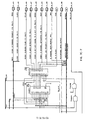
- a synchronizer block diagram is shown in Fig. 1, with corresponding PLL waveforms shown in Fig. 2.
- the synchronizer described herein utilizes a digital phase-locked-loop, a simple model for which is shown in Fig. 3A.
- a first-order loop is controlled by a proportional-gain.
- F(Z) identifies the loop-filter and
- M identifies a loop frequency-divider.
- the box labelled “Window Range” in Fig. 3A varies the loop constant, as will be explained in greater detail below.
- the synchronizer shown in Fig. 1 includes a binary phase-detector PD.
- the phase-error PE bit sequence is processed by a controller to obtain phase-manipulation of the digital-controlled-clock DCC to result in a phase transition to advance or retard the clock time.
- the system shown in Fig. 1, and in greater detail in Figs. 7A-7E, is capable of reducing the available proportional-gain for a given SCLK-to-data-rate ratio. This reduction is obtained by performing phase-shift-correction in a "nonperiodic fashion", as opposed to conventional techniques which correct at periodic positions. Alternatively, a given proportional-gain requires a lower crystal clock rate for implementation.
- Another advantage of the present invention is its ability to disable phase correction when no timing information is available, thereby reducing pattern-dependent jitter.
- the phase-detector PD compares the phase-relation from the digital-controlled-clock DCC to the timing-signal edge every data period 1/f b . This results in a phase-error PE.
- the output of the digital-controlled-clock DCC identified as the received clock signal "rclock" in Fig. 3A, has its frequency reduced by a counter M to obtain the baud-clock BDCC.
- the binary phase-detector PD generates the error signal, indicating whether the edge of the baud clock BDCC is early or late with respect to the incoming "timing-signal".
- the transfer characteristics of the binary phase-detector PD are illustrated in Fig. 3C as m(k1/f b ) vs. phase-error PE.
- the correction "size” is proportional to error magnitude and the step size is self-regulating in the loop.
- error "size” is immaterial and only sign is accounted for.
- a controlled-clock includes a demodulator which performs an integration to obtain the controlled variable, phase in this case, without effecting the order of the loop.
- Phase correction is typically performed in a periodic fashion at a rate which is a fraction of the master clock SCLK.
- a timing-extractor TEX On baseband transceivers, a timing-extractor TEX generates nonperiodic strobes.
- a gating technique is required to avoid miscorrection to the digital-controlled-clock DCC during lack of strobe periods.
- the phase-detector circuitry includes a "strobe-presence" monitor which guarantees one correction per strobe and avoids correction for the lack-of-strobe condition.
- the digital-controlled-clock DCC circuit is capable of placing the correction at a nonperiodic rate, as explained in greater detail below.
- Control commands are issued to the digital-controlled-clock DCC at every strobe by two binary signals.
- a phase-detector signal indicates direction of correction and a "hold-go" signal defines strobe presence.
- the front-end of the digital-controlled-clock DCC receives a sequence of phase error PE bits and integrates them to determine when to effect the phase-manipulation step. This produces instantaneous, impulsive frequency changes.
- Conventional digital-phase-locked-loops have a fixed time-point, or epoch, to apply a step size of either one or a multiple of the SCLK periods.
- the first-order PLL capture range is given by +/- of the inverse of proportional gain PG, where proportional gain PG is the ratio of effected corrections to the total number of possible corrections made.
- the nonperiodic corrections of the quotient PLL of the present invention stretch the "number of possible corrections to actual corrections" ratio, resulting in fractional proportional gains (i.e. ⁇ 1). Small fractional corrections are accumulated over several correction periods.
- the digital-controlled-clock operates on a "quotient" basis at the baud-rate.
- a sequential accumulator "A i " is divided by a divisor constant “K” (called modulous) resulting in a quotient Q i , which may be only 1 or 0, and a remainder R i .
- the value R i -1 is added to a "delta D i " and the operation is repeated. For incremental phase control, this is done by fluctuating the D i value ⁇ 1 around a constant D a , as shown in Fig. 5.
- the waveform Q i displays a sequence of "1" values followed by the appearance of a "0", with patterns depending on the phase error history sequence.
- the rate of zeroes in the waveform Q i is determined by the divisor constant K and by the size of D i and is evident by the patterns created in the R i and A i waveform, as further shown in Fig. 5.
- the remainder R i has a memory effect which slowly fades its value, keeping the quotient Q i at 1. When the remainder is exhausted, a "0" Q i appears.
- An incremental ( ⁇ step) phase is effected by issuing a ⁇ 1 increment on the constant D a at the given baud time (i). Patterns on the A i waveform are extended, or shortened, with corresponding effect in the quotient Q i , and either stop or accelerate a further change of phase.
- the "rclock" output is obtained by gating the crystal-clock with the quotient Q i signal. The rclock frequency is further divided down to the baud-frequency to feed the phase-detector PD. For steady-state frequency-division, D i is maintained at the value D a .
- Absolute phase is obtained after an accumulation of past ⁇ inputs.
- the quotient-factor R is equal to D a /K or, in the example, 12/15.
- Step size applied for correction determines the loop time-constant.
- a speed circuit that varies proportional gain PG depending on circuit conditions is described below.
- Digital phase-locked-loops typically have the problem that the loop proportional gain PG determines the phase control resolution and capture dynamics, i.e., capture-range and lock-time.
- An approach that avoids this disadvantage makes use of a second digital phase-detector called a range-phase-detector RPD.
- the range-phase-detector RPD resolves whether the digital-controlled-clock DCC phase is "in” or "out” of a range, as shown in Fig. 6A.
- Gear-shifting is used to effect eventual larger correction steps.
- the range-phase-detector RPD decision dynamically changes the number of consecutive corrections made per strobe, thus modifying the capture speed and range, as shown in Fig. 6B.
- phase-range is defined as a sector of finite phase-width around a desired range to determine the in or out of range of the phase error PE.
- the range-phase-detector RPD has a binary output indicating the in or out of range of the digital-controlled-clock DCC phase with respect to the incoming strobe.
- Speed modulation in the quotient phase-locked-loop of the present invention effectively changes the slope of the phase-versus-time response of the capture-process.
- Incremental range-phase-detector RPD output is accumulated in a top and bottom saturated integrator which determines the current operating speed, as shown in Fig. 6B.
- Another vital issue to be considered in the application of the present invention is the reduction of pattern noise by gating off the incremental phase error PE.
- the speed-integrator drifts to the fast-mode. For some applications, it is more robust to maintain the current speed for the time-out value TO, i.e. acceptable carrier missed time. If TO is reached, the system is returned to fast-access mode.
- the input signal is processed by a data-detect circuit that enables control circuit operation, as illustrated in Fig. 3A.
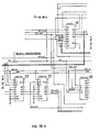
- FIG. 7A-7E An adaptive equalizer controller/PLL timing recovery/data sampler circuit which utilizes the quotient digital-phase-locked-loop concepts of the present invention is shown schematically in Figs. 7A-7E.
- the circuit includes a receiver front end and adaptive equalizer which includes an input transformer 10 with a 1:1 ratio to prevent overloading of the buffers and the equalizer.
- the output of the transformer 10 is provided as one of the inputs to a unity gain buffer and low-pass filter consisting of buffer 12, 2.7K resistor 14 and 47 pF capacitor 16 and having a -3 dB roll-off at a frequency of 1.25 MHz.
- the output of the unity gain buffer is provided to a line equalization high-pass filter which consists of buffer 18 and an input RC consisting of 4.7K resistor 20 and 250 pF capacitor 22.
- the high-pass filter has a -3 dB roll-off at a frequency of 135 KHz.
- the amount of equalization is controlled by binary code at pins C (msb), B and A of component 19 and it's seven associated resistors. Thus, there are eight possible steps, with a "0" binary code equalling a flat response.
- the equalizer output signal from component 24 is provided to a group of input slicers and level translators (see Fig. 7A-5).
- V ath + exceeds 1280 mv
- V0+ and VO-are clamped to 640 millivolts and -640 millivolts, respectively.
- the clamping function is necessary when the circuit operates in the network terminating mode with multiple-terminal nodes TE connected to the bus. Otherwise the nearby TEs would drive the V0+ or the VO-threshold levels above the received signal peaks from the remote TEs, causing detection errors.
- the PNP transistor 42 connected to the negative input pin of component 38 provides the clamping function.
- the output of auto-threshold comparators 32 and 34 is provided to an auto-threshold controller. More specifically, the output of auto-threshold comparator 34 is provided through XOR gate 44 and pipelined through components 46 and 48 (see Fig. 7A-2), its destination being auto-threshold controller ROM 50 (see Fig. 7A-3).
- the coding program "ATHCTL.src" for auto-threshold controller ROM 50 is provided in Appendix A at the end of this specification.
- the signal at pin A3 of ROM 50 is named "TOPP", and, if high, shows the 0+ pulse from the equalizer is either higher than V ath + or the 0- pulse is lower than V ath - (0+ and 0- pulses are exclusive).
- the TOPP signal is used to generate the error feedback control for the loop. Under normal operation, the control loop will "track out” the voltage differences causing TOPP to bounce between 0V and 5V.
- the first qualifier is provided by center estimating ROM 52 (see Fig. 7A-7) and is the sliced output from the 0+ and 0- filters.
- the TOPPM signal also indicates when the input signal has no modulation, i.e. binary 1's imbedded in the input stream. In this case, V ath +, as well as V ath -, retain the previous value during the binary 1's period, resulting in less ripple in the control voltage.
- the second qualifier input to ROM 50 is provided by the adaptive equalizer and is identified as "AEQWDW". This qualifier allows the auto-threshold circuit to operate on the same input signal segments as the adaptive equalizer.
- the third input to ROM 50 is from the frame synchronizer/ lock detector, to be described below, and is identified as "BSLOTS". This signal enables the auto-threshold circuit from the second "B" bit to the bit after the last "B” bit in the B1 and B2 channels.
- the function of the BSLOTS input is to prevent the auto-threshold circuit from responding to other bits which may contain distortion due to bus contention.
- the signal "AEQSPD”, applied to pin A7 of ROM 50, is derived from the frame synchronizer/lock detector, which is set high after frame-in-lock plus eight additional frames, and is used to enable/disable the qualifiers.
- AEQSPD When AEQSPD is set low, the TOPP output is qualified with TOPPM only, so that V ath + or V ath - ramps up at maximum speed.
- TOPP After signal AEQSPD is set high, TOPP is qualified with TOPPM, AEQWDW and BSLOTS, so that the activities of the auto-threshold circuit are limited to a fraction of a bit period within the B channels for rejecting unwanted input imperfections.
- Components 54, 56 and 58 form an error integrator for the control loop.
- the error integrator up/down controlled by the TOPP signal, is enabled during the period defined by the qualifiers.
- the integrator counters either count up if the input signal is less than V ath + or count down if the input signal is more than V ath +. The opposite is true for V ath -.
- the signal TOPP which is applied at pin D3 of ROM 50 and derived from the center estimating ROM 52, is the sliced 0+ filter output. This signal is similar to TOPPM except that there is no output for the 0- input pulses. During the rising edge of the TOPP signal, the integrator's output is transferred to a Sigma/Delta modulator, described below.
- the Sigma/Delta modulator consisting of components 60, 62 and 64 (see Fig. 7A-4), converts the binary output from the integrators 54, 56 and 58 to a 1 bit pulse density modulated PDM signal having a 7.68 MHz sampling frequency.
- the modulator is functionally equivalent to a conventional 6 bit digital-to-analog converter (DAC).
- DAC digital-to-analog converter
- the output of the modulator is available at the "carry” pin, i.e. pin C4, of adder circuit 60.
- the output is then pipelined through component 48 (pin 1D) and converted into a DC control voltage after the RC "T" network consisting of 6.8K resistor 47 and 6800 pF capacitor 49, connected at pin 1Q of component 48.
- the RC time constant is set at 20 microseconds, which is about 4 bit periods.
- the 0+ filter block consisting of components 66, 68, 70 and 72
- the 0-filter block consisting of components 74, 76, 78 and 80
- Each filter block consists of two 1-bit wide moving average filters (5 and 15 sampling points), so there are four filters.
- the filter algorithm sums the numbers of 1's and 0's within the specified window period. If the number of 1's is greater than the number of 0's, then the filter outputs a "1". If the opposite is true, then the filter outputs a "0". Details of the coding algorithm "FTF" are provided in Appendix B at the end of this specification.
- the implementation of the 15-point filters is slightly different from the 5-point filters, in that the 15-point filters utilize counters instead of direct decoding for cost purposes.
- the 5-point filters are utilized for signal detection, i.e., demodulation, purposes.
- the 0+ filter output is available at pin D0 of component 70, while the 0- output is available at pin D0 of component 78.
- These two outputs after being pipelined through component 82, are provided to PROM 84 (see Fig. 7A-7).
- PROM 84 also receives inputs from the 15-point outputs of filters 72 and 80.
- the select pin i.e., pin A4 of PROM 84, selects either the 5-point pair or the 15-point pair to the outputs of PROM 84.
- the select input is connected to V CC such that the 5-point filter outputs are always selected.
- the "RX-DATA” output is the logical “OR" of the 5-point 0+ and 0-filter outputs: if high, input equals 0+ or 0-; if low, input equal binary 1.
- the coding program "FASEL" for the PROM 84 is provided in Appendix C at the end of this specification.
- the 15-point filters serve as the front-end circuitry for the center estimator described below.
- the TOPP and TOPPM signals connected to the auto-thresholder section described above are derived from the 0+ and the 0- filters: if the number of 1's is ⁇ 12 within a 15-point window, then the output is set to 1.
- a front-end set of comparators slice the signal at thresholds determined by a peak detector circuit, typically at one-half of the received signal peak.
- the system is sampled at a rate f s , typically many times the line-rate f b .
- Asynchronous polar pulses P and N are fed with proper phase to the filter circuits using shift registers 66, 68 and 74, 76, respectively. Integration is performed by up-down counters 72 and 80 which are connected in a top/bottom self-stop mode. Circuits 70 and 78 produce integrator control signals based in pulse presence for a time span given by the register length.
- Center estimator ROM 52 contains discrimination logic plus detector circuitry. As stated above, state transition is provided by the FASEL program listing provided in Appendix C.
- control ROM 86 is inlock with a PLL timing recovery circuit to be described below.
- the program coding "AEQCTL.src" for equalizer control ROM 86 is provided in Appendix D at the end of this specification.
- An auto-threshold circuit should be settled-out, e.g., the slicing level of component 34 tracks the peaks of the equalizer output.
- the "DCC-OUT” signal controls the up/down of the error integrator counters 88, 90 and 92 (see Fig. 7B-1).
- the DCC-OUT signal, or digital-controlled-clock DCC output also equals the timing-recovery clock from the PLL or PLL clock available at pin QD of component 85 (see Fig. 7B-2); low to high transitions are normally aligned to the center of the TOPP signal if the input needs no equalization, e.g., short connection between TE and NT.
- the counters 88, 90 and 92 are enabled when the "TANDT" signal is high. This signal is available by ANDing the TOPP and TOPPM signals. If the auto-threshold circuit is not settled, the TANDT signal will have either no output or a full output such that there will be no up or down counts passed on to the counters. In the case of no output, the counters are not enabled. In the case of a full output, the up counts will be equal to the down counts since the DCC-OUT signal is centered about the enable window TANDT. In other words, the adaptive equalizer is automatically disabled when the threshold is not settled.
- the TOPP signal will be centering at the PLL clock rising edges so that up counts equal down counts and no step changes are passed onto component 19 (Fig. 7A-1).
- Counters 88, 90 and 92 form a dual speed (8 or 12-bit) error integrator.
- the integrator has a high tracking-rate when the circuit starts receiving signal after the reset due to the INFO 0 signal, and a low tracking-rate after "frame in-lock" plus 8 good frames.
- the selection is controlled by the AEQSPD signal derived from the frame synchronizer/lock detector.
- the AEQWDW and BSLOTS signals are enabled.
- the AEQWDE signal is available at pin A0 of component 86 (see Fig. 7B-5) and is derived from the PLL clock, with a width of window equal to 25% of a bit period, with centering at PLL clock rising-edges.
- the BSLOTS signal is available at pin A4 of component 86.
- Component 94 is a step-update D-latch which is clocked after low-to-high transitions of the TOPP signal so that distortion at the equalizer output due to injection charge of component 19 during step changes is forced to the center of 0+ bit cells. Otherwise, detection errors are caused.
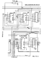
- the quotient algorithm digital-phase-locked-loop portion of the circuit receives the timing signal strobe and the BIO signal as inputs.
- a binary phase detector with hold-go gating is implemented by using a function of the strobe (F-strobe) to latch a counter that is cycling through a baud.
- F-strobe is processed by control machine 96 (see Fig. 7B-4) which avoids correction for a no-strobe condition.
- Components 98 and 100 are no-strobe time-out circuits.
- Speed value is calculated on a saturating (bi-directional) speed counter 102 and altered only when triggered by a strobe on a baud period enabled by the BIO signal. Speed is input to ROM 96 to generate the hold/go signal on a fast or slow basis to feed the digital-controlled-clock DCC. The speed value is fed into the F-strobe monitor which creates a gating signal to the digital-controlled-clock DCC allowing incremental phase to be executed for "x" number of times dependent on the speed.
- digital-controlled-clock 104 and latch 106 obtain the quotient-digital-controlled-clock and output Q I which gates the SCLK signal to result in RCLOCK.
- the RCLOCK signal is divided by divider 108,110 (see Fig. 7B-3) to quantify the phase position on a baud interval (baud rate recovered clock) for the binary phase-detector using the most significant bits and the range-phase-detector RPD circuit using a magnitude or-phase-error-comparator.
- the no-strobe decoder 98, 100 used in this portion of the circuit increases the phase-lock-loop gain when seven consecutive missing synchronizing-strobes to the PLL are detected. Otherwise, the PLL would not be able to track an input with excess frequency-offset. The extreme case would be info 3 or 4 without marks at the B, D and SF channels.
- a received-data sampler and clocks switching logic utilizes ROMs 114 and 116, the coding algorithms for which "SCLKP.src” and “SCPDEC.src” are provided in Appendices I and J, respectively, at the end of this specification.
- the first sampler clock i.e., pins LD and CK of component 118 (see Fig. 7B-5)
- the "Signal Eye” at the filter output is sampled at maximum "eye” opening.
- the second sampler-clock i.e., pins LD and CK of component 120 (see Fig. 7B-6)
- the third sampler clock i.e., pin CK of component 122, experiences a 4.5 pipeline delay after the PLL clock.
- the delay section i.e., the tap point at component 124, will effect the alignment of the TX zero-crossings to the RX zero crossings.
- the first sampler clock i.e., pins LD and CK of component 118
- the second sampler clock i.e., pins LD and CK of component 120, as derived from a free-running counter with frequency synchronized to the TX bit clock. If the PLL is out-of-lock, the counter is phase synchronized to the PLL clock with rising edges equal 20 pipeline delay (half of a bit period) after rising edges of the PLL clock.
- the PLL If the PLL is in-lock, the synchronizing link to the PLL is defeated and the counter left free-running and the frequency is synchronized to TX bit clock. Thus, it samples at maximum opening of the Signal Eye for the first sampler 118.
- the third sampler is clock 122. Therefore, the received data output has the same timing as the transmitter.
- the first sampler clock 118 has a 0.5 pipeline delay after the fixed timing clock, i.e., pin A2 of component 114, i.e., a fixed relationship to the TX bit clock.
- the second sampler clock 120 experiences a 1 pipeline delay after the fixed timing clock to allow data to pass onto the third sampler.
- the third sampler clock 122 is connected to the TX bit clock so that the receive data output has the same timing as the transmitter.
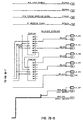
- components 128, 130, 132 and 134 form a frame trigger pulse decoder.
- components 136, 138, 140, 142, 144 and 146 form a frame synchronizer/lock detector.
- Three consecutive good frames plus the PLL in-lock equals a frame-in-lock.
- PROM 140 (see Fig. 7C-3) also decodes the polarity of the M bits (super frame) for generating the M-clock in the TE mode.
- info recognition criteria are as follows:
- a D-channel access/E-channel logic circuit is formed by components 160, 162, 164, 166, 168, 170, 172, 174, 176 and 178 (see Figs. 7C-5, 7C-6 and 7C-7).
- Components 160 and 162 are a D/E/SF transmit-data decoder.
- Pins D3 and D2 of component 162 provide the E-bit outputs which control "C" counter 164.
- Pin 3Q of component 160 is a pipelined E-bit output which drives component 176 for transmission E-bit data input to the transmitter in the NT mode.
- Pin 5Q of component 160 is the super-frame transmit-data output for NT mode only.
- this pin decodes the inverted FA/N bits from the NT output to qualify the generation of the M-clock.
- Components 164 and 166 form a "C" counter, with pin D1 of component 166 high if the D-channel is available, i.e., "C" count is ⁇ the current priority level. Both the class and the priority signals are inputs to this counter. The circuit is disabled if the frame is out-of-lock.
- Components 168, 170, 172 and 174 combine to form a D-channel flag-decoder.
- the "LSTD" signal or last-transmitted D-bit from the local transmitter, on pin 1Q of component 174 feeds component 176 for error flag generation.
- the D-channel access is terminated immediately, i.e., the DACT signal on pin A1 of component 176 goes low.
- the transmitter sends binary 1s in the D-channel afterward regardless of the state of the transmitter data input. There are no more DSHT (D-channel data shift/enable) pulses to the outside world for requesting data. Priority remains the original value, i.e., high priority.
- the "C8" signal at pin 3Q of component 174 goes high if D-channel transmitted data was eight consecutive 1's. After this flag, the D-channel access is deactivated. This is similar to the closing flag case except there are no priority changes.
- the D-channel request input "DREG" at pin A8 of component 176 goes high if TE wants to access the D-channel. If pin A5 of component 176 is high, i.e. the D-channel is available, and DREQ is high, then DACT is high showing that the D-channel is activated. If any of the error flags (E ⁇ >D, CFLG, C8) are detected, then DACT goes low showing that the D-channel is deactivated. Priority output at pin 5Q of component 178 is high (low priority) if deactivation is due to CFLG. If frame is out-of-lock during activation, then the D-channel access is terminated immediately the same way as caused by other flags. The implementation is achieved by resetting the D-channel circuit, including the C counter, to its power-up state. In other words, D-channel access is only possible when the frame synchronizer is in-lock.
- activate/deactivate logic is provided by components 180, 182, 184, 186, 188 and 190.
- the coding algorithm "ADLGC.src" for ROMs 180, 182 and 184 is provided in Appendix K at the end of this specification.
- Appendix L provides the recommended subroutines for external up and input latch circuit for AR (Activation Request), DR (Deactivation Request) and T31XP (Timer 3/1 expiry).
- I124 indicates the receiving of INFO1(NT) or INFO2/4(TE). This signal is sent to the external microprocessor through the uwire for activation acknowledgment.
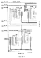
- Components 196 and 198 form a superframe counter controller.
- Component 200 (sec Fig. 7D-5) provides superframe enable/disable and clock switching functions.
- the SFMC signal is switched to receive it's input from the frame synchronizer in the TE mode (i.e., pin D3 of component 200 is not active).
- the M clock provides timing information to the transmit data processor 202 for encoding the M(S1) bit.
- Pin D1 of component 200 derives a "1 out of 5" frame sequence from the outputs of counter 192, 194 for generating the Q clock SFQC.
- the Q clock is enabled when Superframe timing is in-lock. This clock feeds two elements: transmit data-rocessor 202 and frame synchronizer/lock detector 204 (see Fig. 7D-6).
- the first connection provides timing information to the transmitter for encoding the Fa/N (INFO4) or Fa/L (INFO3) bits.
- the second connection forbids the frame locking circuit 204 from responding to missing frame trigger pulses during superframes.
- the S2 signal is the data output in the TE mode and can be decoded from RXC-DTA with RX-S2.
- the signal is also the S2 data-input to the NT transmitter.
- a transmit data processor/encoder is formed by components 206, 202, 208, 204, 210, 212, 214, 216 and 218.
- the B-channel data path is enabled by signals BSHT and TXF8 at pins 2Q and 1Q, respectively, of component 218: channel B1 is selected when TXF8 is high and BSHT is high; channel B2 is selected when TXF82 is low and BSHT is high.
- the TXF8 signal also provides half-frame timing.
- the DRX signal at pin A4 of component 202 and the E-bit TX data input is connected to the D-channel RX output and multiplexed by component 202 into the TX data path.
- Pin A7 of component 202 provides the superframe data input (TE mode only).
- the transmitter In the NT mode, the transmitter is frame synchronized to an external source (U-Interface) by either shortening (39 counts) or widening (41 counts) the last L bit period. In the TE mode, the transmitter is frame synchronized to the RX-frame with a 2-bit offset.
- components 220 and 222 provide TE/NT select.
- the receiver is configured as adaptive timing mode (similar to receiver in TE mode) for receiving asynchronous Info1 signal. After INFO1 is recognized, the receiver is switched back to normal mode.
- the NT adaptive timing mode if NT changes from the G3 state to the G2 state, due to loss of framing or upon receiving INFO0, pin 3Q of component 222 will issue a low-going pulse for resetting the PLL locking circuitry, thus causing phase re-estimation of the second sampling clock.
- an NT frame synchronizer is formed by components 222, 224, 226, 228, 232, 234 and 236.
- the NT receiving clock NTRCLK, pin QC of component 224 is at 192KHz and is generated by dividing 7.68MHz with a modulo of 40 in components 232 and 234. For each bit period, there are forty 7.68MHz clocks.
- the NT frame sync input signal NTFSYN at pin B of components 224 is provided for an external 8KHz sync signal to synchronize the framing of the transmitter.
- the transmitter frame clock provided at pin A9 of component 236 is free running at the sub-multiple (/40, 40 clocks per bit; and then /48, bits per frame) of the crystal frequency (7.68MHz). If an external sync-signal is applied to this input, then the counters 232, 234 will either add or subtract a count during the last bit of each frame until the frame-timing is frequency locked to the positive edges of the external input.
- the coding algorithm component 236 does not allow consecutive opposite changes (e.g., 39 in one frame and 41 in the next frame): the counters have to step through the normal state (/40) before the next opposite change.
- the counters 115, 117 (Fig. 7B) used in the sampler-clock processor are also frequency-locked to the external sync signal in NT adaptive timing mode. This is accomplished by the signal BC3940 connecting between pin D2 of component 236 and pin ENP of component 117.
- a system clock-generator is formed by components 238, 240, 242, 244, 246 and 248.
- the clock input is 15.36 MHz crystal in the TE mode and 15.36 MHz external input in the NT mode from the U-Interface.
- the fixed timing sampling clock signal FTMCLK at pin QB of component 248 can be moved to other taps for different RX sampling timings; this connection only affects NT Fixed-Timing mode.
Description

| X' Former Secondary | Eq O/P | Vath+ | VO+ |
| 1 Vpeak (+2.5dB) | 2.33Vpeak | 2.33V | 0.64V |
| 0.89Vpeak (+1.5dB) | 2.07Vpeak | 2.07V | 0.64V |
| 0.75Vpeak ( 0 dB) | 1.74Vpeak | 1.74V | 0.64V |
| 0.55Vpeak (-2.7dB) | 1.28Vpeak | 1.28V | 0.64V |
| 0.50Vpeak (-3.5dB) | 1.17Vpeak | 1.17V | 0.58V |
| 0.32Vpeak (-7.5dB) | 0.74Vpeak | 0.74V | 0.37V |
| 0.09Vpeak (-18.0dB) | 0.22Vpeak | 0.22V | 0.11V |
| 0Vpeak | 0Vpeak | 0.22V | 0.11V |
| Note: Vath- = -Vath+, VO- = -VO+ |
| B1 channel: | B (pin D1 of component 140)=high |
| F8 (pin D4 of component 140)=high | |
| B2 channel: | B (pin D1 of component 140)=high |
| F8 (pin D4 of component 140)=low | |
| S2 channel: | S2 (pin D0 of component 140)=high |
| D channel: | Decoded as described below |
| SF channel: | Decoded as described below |
| Note: | F8 also provides half-frame timing |
- INFO 0:
- If no 0+ or 0- pulses for 64 data bits, BIO (bar info 0) goes low at frame boundaries.
- INFO 1:
- NT mode, 8 consecutive "0011xxxx" frame received, "x" denotes either 0 or 1, the two consecutive 0s must be opposite in polarity and consistent through the 8 frames.
- INFO ANY:
- Circuit detects Info Any after receiving two opposite "0" pulses ("0+, 0-" or "0-, 0+"). If other info types can be unambiguously recognized the detector will flag the actual info types instead. Normally, Info Any indicates the receiving of I2, I3 or I4 when the framing circuit is not in-lock, i.e., loss of framing or before locking.
- INFO 3:
- NT mode, frame in-lock
- INFO 2:
- TE mode, frame in-lock, "A" bit=binary 0 (0+ or 0-)
- INFO 4:
- TE mode, frame in-clock, "A" bit=
binary 1


Claims (6)
- A quotient digital phase locked loop, comprising:characterized in that the digital controlled clock includes quotient processor means which divides a sequential accumulator value by a divisor constant each period defined by a crystal clock input to the digital controlled clock, the division resulting in a quotient value and a remainder value, the quotient value being only 0 or 1, the remainder value for successive divisions being added until the sum of the remainder values equals or exceeds a predetermined value, the qoutient value equals 0 only when the remainder value sum equals or exceeds the predetermined value, resulting in a quotient value bit stream comprising a sequence of 1s and nonperiodic 0s, the quotient value bit stream being utilized to effect nonperiodic phase manipulation of the baud clock signal.(a) a binary phase detector means (PD) which compares an incoming signal to an internally-generated baud clock signal to provide a phase error bit sequence which indicates wether the phase of the incoming signal is early or late with respect to the phase of the baud clock signal; and(b) a digital controlled clock (DCC) which integrates the phase error bit sequence to effect nonperiodic phase manipulation of the baud clock signal,
- A quotient digital phase locked loop as in claim 1 and further including a range-phase-detector (RPD) which generates an output indicative of wether the phase of the output of the digital controlled clock (DCC) is within a predetermined phase range.
- A quotient digital phase locked loop as in claim 2 wherein the range-phase-detector output is utilized to dynamically change the frequency of phase manipulation of the baud clock signal.
- A quotient digital phase locked loop as in claim 1 and further including means for avoiding phase manipulation during a lack-of-strobe condition.
- A quotient digital phase locked loop as in claim 1 and further including means for disabling phase manipulation when no timing information is available such that pattern dependant noise is reduced.
- A quotient digital phase locked loop as in claim 1 and further including means for dynamically varying the loop time constant to obtain wide capture range and low jitter.
Applications Claiming Priority (2)
| Application Number | Priority Date | Filing Date | Title |
|---|---|---|---|
| US108371 | 1987-10-14 | ||
| US07/108,371 US4862485A (en) | 1987-10-14 | 1987-10-14 | Quotient phase-shift processor for digital phase-locked-loops |
Publications (3)
| Publication Number | Publication Date |
|---|---|
| EP0311973A2 EP0311973A2 (en) | 1989-04-19 |
| EP0311973A3 EP0311973A3 (en) | 1991-03-27 |
| EP0311973B1 true EP0311973B1 (en) | 1998-05-13 |
Family
ID=22321834
Family Applications (1)
| Application Number | Title | Priority Date | Filing Date |
|---|---|---|---|
| EP88116847A Expired - Lifetime EP0311973B1 (en) | 1987-10-14 | 1988-10-11 | Quotient phase-shift processor for digital phase-licked-loops |
Country Status (5)
| Country | Link |
|---|---|
| US (1) | US4862485A (en) |
| EP (1) | EP0311973B1 (en) |
| JP (1) | JPH021621A (en) |
| CA (1) | CA1291539C (en) |
| DE (1) | DE3856178T2 (en) |
Families Citing this family (46)
| Publication number | Priority date | Publication date | Assignee | Title |
|---|---|---|---|---|
| JP2693784B2 (en) * | 1988-07-05 | 1997-12-24 | 株式会社リコー | Image forming device |
| US5341405A (en) * | 1991-06-11 | 1994-08-23 | Digital Equipment Corporation | Data recovery apparatus and methods |
| US5412691A (en) * | 1991-06-28 | 1995-05-02 | Digital Equipment Corporation | Method and apparatus for equalization for transmission over a band-limited channel |
| US5255287A (en) * | 1991-06-28 | 1993-10-19 | Digital Equipment Corporation | Transceiver apparatus and methods |
| US5241285A (en) * | 1991-10-03 | 1993-08-31 | Apogee Electronics Corporation | Phase locked loop reference slaving circuit |
| JP3241079B2 (en) * | 1992-02-24 | 2001-12-25 | 株式会社日立製作所 | Digital phase locked loop |
| US5408473A (en) * | 1992-03-03 | 1995-04-18 | Digital Equipment Corporation | Method and apparatus for transmission of communication signals over two parallel channels |
| JPH0795056A (en) * | 1993-05-10 | 1995-04-07 | Internatl Business Mach Corp <Ibm> | Variable frequency standard clock formation device |
| US5832048A (en) * | 1993-12-30 | 1998-11-03 | International Business Machines Corporation | Digital phase-lock loop control system |
| US5493243A (en) * | 1994-01-04 | 1996-02-20 | Level One Communications, Inc. | Digitally controlled first order jitter attentuator using a digital frequency synthesizer |
| US5581585A (en) * | 1994-10-21 | 1996-12-03 | Level One Communications, Inc. | Phase-locked loop timing recovery circuit |
| US5561660A (en) * | 1995-04-05 | 1996-10-01 | Silicon Systems, Inc. | Offset and phase correction for delta-sigma modulators |
| US5701099A (en) * | 1995-11-27 | 1997-12-23 | Level One Communications, Inc. | Transconductor-C filter element with coarse and fine adjustment |
| US6249557B1 (en) | 1997-03-04 | 2001-06-19 | Level One Communications, Inc. | Apparatus and method for performing timing recovery |
| US6229863B1 (en) | 1998-11-02 | 2001-05-08 | Adc Telecommunications, Inc. | Reducing waiting time jitter |
| US6696828B2 (en) | 1999-11-30 | 2004-02-24 | Kabushiki Kaisha Toshiba | Integrated circuit and lot selection system therefor |
| KR100930988B1 (en) * | 2001-04-16 | 2009-12-10 | 톰슨 라이센싱 | A phase tracking system and method |
| US7031687B2 (en) | 2001-04-18 | 2006-04-18 | Nokia Corporation | Balanced circuit arrangement and method for linearizing such an arrangement |
| US6704329B2 (en) * | 2001-05-08 | 2004-03-09 | Path 1 Network Technologies Inc. | Minimizing the effect of jitter upon the quality of service operation of networked gateway devices |
| US6633185B2 (en) * | 2001-10-16 | 2003-10-14 | Altera Corporation | PLL/DLL circuitry programmable for high bandwidth and low bandwidth applications |
| DE10245556B3 (en) * | 2002-09-30 | 2004-04-22 | Siemens Audiologische Technik Gmbh | Hearing aid or hearing aid system with a clock generator and method for their operation |
| US7768981B1 (en) | 2005-06-14 | 2010-08-03 | Marvell International Ltd. | Bluetooth coexistence timing synchronization |
| WO2007066818A1 (en) * | 2005-12-09 | 2007-06-14 | Sony Corporation | Music edit device and music edit method |
| DE102006011285B4 (en) * | 2006-03-10 | 2019-09-05 | Intel Deutschland Gmbh | Oscillating circuit arrangement with digital control, method for generating a vibration signal and digital phase locked loop with the resonant circuit arrangement |
| KR101284943B1 (en) * | 2006-06-30 | 2013-07-10 | 엘지디스플레이 주식회사 | Method for fabricating mold |
| US8509371B2 (en) * | 2009-09-29 | 2013-08-13 | Analog Devices, Inc. | Continuous-rate clock recovery circuit |
| US8681917B2 (en) | 2010-03-31 | 2014-03-25 | Andrew Llc | Synchronous transfer of streaming data in a distributed antenna system |
| US9495285B2 (en) | 2014-09-16 | 2016-11-15 | Integrated Device Technology, Inc. | Initiating operation of a timing device using a read only memory (ROM) or a one time programmable non volatile memory (OTP NVM) |
| US9553570B1 (en) | 2014-12-10 | 2017-01-24 | Integrated Device Technology, Inc. | Crystal-less jitter attenuator |
| US9369139B1 (en) | 2015-02-14 | 2016-06-14 | Integrated Device Technology, Inc. | Fractional reference-injection PLL |
| US9336896B1 (en) | 2015-03-23 | 2016-05-10 | Integrated Device Technology, Inc. | System and method for voltage regulation of one-time-programmable (OTP) memory programming voltage |
| US9455045B1 (en) | 2015-04-20 | 2016-09-27 | Integrated Device Technology, Inc. | Controlling operation of a timing device using an OTP NVM to store timing device configurations in a RAM |
| US9362928B1 (en) * | 2015-07-08 | 2016-06-07 | Integrated Device Technology, Inc. | Low-spurious fractional N-frequency divider and method of use |
| US9954516B1 (en) | 2015-08-19 | 2018-04-24 | Integrated Device Technology, Inc. | Timing device having multi-purpose pin with proactive function |
| US9590637B1 (en) | 2015-08-28 | 2017-03-07 | Integrated Device Technology, Inc. | High-speed programmable frequency divider with 50% output duty cycle |
| US9847869B1 (en) | 2015-10-23 | 2017-12-19 | Integrated Device Technology, Inc. | Frequency synthesizer with microcode control |
| US9614508B1 (en) | 2015-12-03 | 2017-04-04 | Integrated Device Technology, Inc. | System and method for deskewing output clock signals |
| US10075284B1 (en) | 2016-01-21 | 2018-09-11 | Integrated Device Technology, Inc. | Pulse width modulation (PWM) to align clocks across multiple separated cards within a communication system |
| US9852039B1 (en) | 2016-02-03 | 2017-12-26 | Integrated Device Technology, Inc | Phase locked loop (PLL) timing device evaluation system and method for evaluating PLL timing devices |
| US9859901B1 (en) | 2016-03-08 | 2018-01-02 | Integrated Device Technology, Inc. | Buffer with programmable input/output phase relationship |
| US9692394B1 (en) | 2016-03-25 | 2017-06-27 | Integrated Device Technology, Inc. | Programmable low power high-speed current steering logic (LPHCSL) driver and method of use |
| US9698787B1 (en) | 2016-03-28 | 2017-07-04 | Integrated Device Technology, Inc. | Integrated low voltage differential signaling (LVDS) and high-speed current steering logic (HCSL) circuit and method of use |
| US9581973B1 (en) | 2016-03-29 | 2017-02-28 | Integrated Device Technology, Inc. | Dual mode clock using a common resonator and associated method of use |
| US9954541B1 (en) | 2016-03-29 | 2018-04-24 | Integrated Device Technology, Inc. | Bulk acoustic wave resonator based fractional frequency synthesizer and method of use |
| US9654121B1 (en) | 2016-06-01 | 2017-05-16 | Integrated Device Technology, Inc. | Calibration method and apparatus for phase locked loop circuit |
| CN107508596B (en) * | 2017-09-04 | 2020-06-23 | 中国电子科技集团公司第四十一研究所 | Multi-loop phase-locked circuit with auxiliary capturing device and frequency presetting method |
Family Cites Families (8)
| Publication number | Priority date | Publication date | Assignee | Title |
|---|---|---|---|---|
| DE2413604A1 (en) * | 1974-03-21 | 1975-09-25 | Blaupunkt Werke Gmbh | PHASE-LOCKED REGULAR LOOP |
| US3983498A (en) * | 1975-11-13 | 1976-09-28 | Motorola, Inc. | Digital phase lock loop |
| US4400817A (en) * | 1980-12-30 | 1983-08-23 | Motorola, Inc. | Method and means of clock recovery in a received stream of digital data |
| US4385396A (en) * | 1981-06-05 | 1983-05-24 | Phillips Petroleum Company | NRZ Digital data recovery |
| US4534044A (en) * | 1983-05-02 | 1985-08-06 | Honeywell Information Systems Inc. | Diskette read data recovery system |
| US4577163A (en) * | 1984-07-09 | 1986-03-18 | Honeywell Inc. | Digital phase locked loop |
| US4633193A (en) * | 1985-12-02 | 1986-12-30 | At&T Bell Laboratories | Clock circuit synchronizer using a frequency synthesizer controlled by a frequency estimator |
| US4713630A (en) * | 1986-07-29 | 1987-12-15 | Communications Satellite Corporation | BPSK Costas-type PLL circuit having false lock prevention |
-
1987
- 1987-10-14 US US07/108,371 patent/US4862485A/en not_active Expired - Lifetime
-
1988
- 1988-10-11 DE DE3856178T patent/DE3856178T2/en not_active Expired - Lifetime
- 1988-10-11 EP EP88116847A patent/EP0311973B1/en not_active Expired - Lifetime
- 1988-10-13 CA CA000579992A patent/CA1291539C/en not_active Expired - Fee Related
- 1988-10-14 JP JP63257471A patent/JPH021621A/en active Pending
Also Published As
| Publication number | Publication date |
|---|---|
| EP0311973A3 (en) | 1991-03-27 |
| US4862485A (en) | 1989-08-29 |
| JPH021621A (en) | 1990-01-05 |
| DE3856178T2 (en) | 1998-12-17 |
| EP0311973A2 (en) | 1989-04-19 |
| CA1291539C (en) | 1991-10-29 |
| DE3856178D1 (en) | 1998-06-18 |
Similar Documents
| Publication | Publication Date | Title |
|---|---|---|
| EP0311973B1 (en) | Quotient phase-shift processor for digital phase-licked-loops | |
| US4873700A (en) | Auto-threshold/adaptive equalizer | |
| CA2130871C (en) | Method and apparatus for a phase-locked loop circuit with holdover mode | |
| US7315596B2 (en) | Interpolator based clock and data recovery (CDR) circuit with digitally programmable BW and tracking capability | |
| CA1284361C (en) | Analog phase locked loop | |
| US6310521B1 (en) | Reference-free clock generation and data recovery PLL | |
| US4827225A (en) | Fast locking phase-locked loop utilizing frequency estimation | |
| US7688887B2 (en) | Precision adaptive equalizer | |
| US8537957B2 (en) | Clock synchroniser | |
| US6683930B1 (en) | Digital phase/frequency detector, and clock generator and data recovery PLL containing the same | |
| US6760389B1 (en) | Data recovery for non-uniformly spaced edges | |
| US20100085086A1 (en) | Digital Frequency Detector | |
| US6927611B2 (en) | Semidigital delay-locked loop using an analog-based finite state machine | |
| JPH0824261B2 (en) | PLL monitoring circuit | |
| JPH03132117A (en) | Phase frequency comparator | |
| US4930142A (en) | Digital phase lock loop | |
| US5859551A (en) | Digital PLL circuit | |
| US5036525A (en) | Adaptive equalizer | |
| JPH0744449B2 (en) | Digital phase lock loop circuit | |
| US6362693B2 (en) | Frequency detection method for adjusting a clock signal frequency and a frequency detector circuit for carrying out the method | |
| US6333678B1 (en) | Method and apparatus for agile phase noise filtering using phase locked loops | |
| US6337650B1 (en) | System and method for regenerating clock signal | |
| JP2004515957A (en) | Phase locked loop for recovering clock signal from data signal | |
| US4888790A (en) | Timing recovery system using bipolar-pattern center estimator | |
| JP3313318B2 (en) | PLL circuit |
Legal Events
| Date | Code | Title | Description |
|---|---|---|---|
| PUAI | Public reference made under article 153(3) epc to a published international application that has entered the european phase |
Free format text: ORIGINAL CODE: 0009012 |
|
| AK | Designated contracting states |
Kind code of ref document: A2 Designated state(s): DE FR GB IT NL |
|
| PUAL | Search report despatched |
Free format text: ORIGINAL CODE: 0009013 |
|
| AK | Designated contracting states |
Kind code of ref document: A3 Designated state(s): DE FR GB IT NL |
|
| 17P | Request for examination filed |
Effective date: 19910905 |
|
| 17Q | First examination report despatched |
Effective date: 19930524 |
|
| GRAG | Despatch of communication of intention to grant |
Free format text: ORIGINAL CODE: EPIDOS AGRA |
|
| GRAG | Despatch of communication of intention to grant |
Free format text: ORIGINAL CODE: EPIDOS AGRA |
|
| GRAH | Despatch of communication of intention to grant a patent |
Free format text: ORIGINAL CODE: EPIDOS IGRA |
|
| GRAH | Despatch of communication of intention to grant a patent |
Free format text: ORIGINAL CODE: EPIDOS IGRA |
|
| GRAA | (expected) grant |
Free format text: ORIGINAL CODE: 0009210 |
|
| AK | Designated contracting states |
Kind code of ref document: B1 Designated state(s): DE FR GB IT NL |
|
| PG25 | Lapsed in a contracting state [announced via postgrant information from national office to epo] |
Ref country code: IT Free format text: LAPSE BECAUSE OF FAILURE TO SUBMIT A TRANSLATION OF THE DESCRIPTION OR TO PAY THE FEE WITHIN THE PRESCRIBED TIME-LIMIT;WARNING: LAPSES OF ITALIAN PATENTS WITH EFFECTIVE DATE BEFORE 2007 MAY HAVE OCCURRED AT ANY TIME BEFORE 2007. THE CORRECT EFFECTIVE DATE MAY BE DIFFERENT FROM THE ONE RECORDED. Effective date: 19980513 Ref country code: FR Free format text: LAPSE BECAUSE OF FAILURE TO SUBMIT A TRANSLATION OF THE DESCRIPTION OR TO PAY THE FEE WITHIN THE PRESCRIBED TIME-LIMIT Effective date: 19980513 Ref country code: NL Free format text: LAPSE BECAUSE OF FAILURE TO SUBMIT A TRANSLATION OF THE DESCRIPTION OR TO PAY THE FEE WITHIN THE PRESCRIBED TIME-LIMIT Effective date: 19980513 |
|
| REF | Corresponds to: |
Ref document number: 3856178 Country of ref document: DE Date of ref document: 19980618 |
|
| NLV1 | Nl: lapsed or annulled due to failure to fulfill the requirements of art. 29p and 29m of the patents act | ||
| EN | Fr: translation not filed | ||
| PLBE | No opposition filed within time limit |
Free format text: ORIGINAL CODE: 0009261 |
|
| STAA | Information on the status of an ep patent application or granted ep patent |
Free format text: STATUS: NO OPPOSITION FILED WITHIN TIME LIMIT |
|
| 26N | No opposition filed | ||
| PGFP | Annual fee paid to national office [announced via postgrant information from national office to epo] |
Ref country code: GB Payment date: 20010921 Year of fee payment: 14 |
|
| REG | Reference to a national code |
Ref country code: GB Ref legal event code: IF02 |
|
| PG25 | Lapsed in a contracting state [announced via postgrant information from national office to epo] |
Ref country code: GB Free format text: LAPSE BECAUSE OF NON-PAYMENT OF DUE FEES Effective date: 20021011 |
|
| GBPC | Gb: european patent ceased through non-payment of renewal fee |
Effective date: 20021011 |
|
| PGFP | Annual fee paid to national office [announced via postgrant information from national office to epo] |
Ref country code: DE Payment date: 20071130 Year of fee payment: 20 |