EP0312193A2 - Code correlation arrangement - Google Patents
Code correlation arrangement Download PDFInfo
- Publication number
- EP0312193A2 EP0312193A2 EP88306672A EP88306672A EP0312193A2 EP 0312193 A2 EP0312193 A2 EP 0312193A2 EP 88306672 A EP88306672 A EP 88306672A EP 88306672 A EP88306672 A EP 88306672A EP 0312193 A2 EP0312193 A2 EP 0312193A2
- Authority
- EP
- European Patent Office
- Prior art keywords
- code
- clock
- phase
- analogue
- bit
- Prior art date
- Legal status (The legal status is an assumption and is not a legal conclusion. Google has not performed a legal analysis and makes no representation as to the accuracy of the status listed.)
- Granted
Links
Images


Classifications
-
- H—ELECTRICITY
- H04—ELECTRIC COMMUNICATION TECHNIQUE
- H04L—TRANSMISSION OF DIGITAL INFORMATION, e.g. TELEGRAPHIC COMMUNICATION
- H04L7/00—Arrangements for synchronising receiver with transmitter
- H04L7/04—Speed or phase control by synchronisation signals
- H04L7/041—Speed or phase control by synchronisation signals using special codes as synchronising signal
- H04L7/043—Pseudo-noise [PN] codes variable during transmission
Definitions
- This invention relates to a code correlation arrangement.
- a known correlation arrangement includes a low pass filter for an incoming analogue signal and a digital code generator, the output of which is multiplied by the filtered signal.
- the analogue resultant is sampled at a rate appropriate to the noise bandwidth and then digitally filtered to reduce noise. It may be noted that a small amount of aliasing will occur due to sampling of the spread noise.
- both the lowpass filtered analogue signal and the code generator output can be sampled before they are digitally multiplied together, instead of sampling the analogue multiplier resultant. Sampling before a digital multiplier will produce an identical result to sampling after an analogue multiplier.
- a code correlation arrangement comprising clock means for sampling an analogue input signal, means for generating a digital code sequence, means for clocking the code generating means synchroniously with the sampling of the analogue input signal, means for digitally multiplying the code sequence with the sampled analogue signal, means for digitally filtering the output of the multiplying means, and means for controlling phase tracking of an incoming code phase in the analogue signal by the code generating means.
- the means for controlling the clock phase of the code generating means comprises a numerically controlled oscillator (NCO) having a frequency control input dependent on the required code phase, the NCO being clocked by the sampling clock, and means for presenting a predetermined bit of the NCO digital output as the clock signal for the code generating means.
- NCO numerically controlled oscillator
- an analogue signal modulated with coded information is passed through a low-pass filter 10 and applied to a sampling circuit 11.
- the sampled signal is then digitally multiplied with a synchronous code in multiplier 12.
- the output of multiplier 12 is finally passed through a digital filter 13 the output of which consists of the correlation samples.
- the synchronous code applied to multiplier 12 is produced by a code generator 14 which is clocked synchronously with the sample clock applied to circuit 11.
- the code generator In order to maintain an accurate phase track of the incoming code phase the code generator must follow the incoming code phase. In other words, there must be provision for adjusting the phase of the locally produced code and therefore the phase of the code generator clock, relative to the sampling clock.
- phase samples from a numerically controlled oscillator (NCO) 15 clocked with the sampling clock.
- NCO numerically controlled oscillator
- the generated phase samples are then quantised to one bit, is then used to clock the code generator in such a way that a clock will occur every sample time that the NCO phase passes 2 ⁇ . It is evident that the sample clock must exceed or at least equal twice the highest code Doppler frequency if output clocks are not to be missed.
- an inverter 16 to invert the most significant bit (MSB) before applying it to the code generator 14. Finite NCO accumulator length will result in reduced frequency resolution.. The phase ramp will always be linear, implying that there will be no phase jitter.
- the basic up-converter arrangement utilises a fast clock applied to a high frequency divider 20 near to the required output frequency.
- the divider 20 is implemented as a very fast counter producing an m-bit word in paralleloutput form.
- the sample rate of this ramp is thus approximately equal to the high frequency clock, e.g. the sample clock of Figure 1.
- the high frequency clock is also fed to a divider 21 to produce a slow clock which drives a slow running NCO 22.
- the output of NCO 22, which is also an m -bit word, is added to the output of divider 20 in a parallel adder 23.
- the resultant m -bit sum is used to address a ROM 24 which provides a digital representation of a sine wave.
- the technique may be used to generate the sampled code clock by using some simplifications.
- the fast phase ramp may be generated by dividing the sample clock by 2. Alternate output samples of 0 or ⁇ will thus result. This represents a phase ramp of half the sample frequency. The ramp must therefore be slowed by subtracting an NCO phase ramp output.
- the required code clock waveform may be obtained by truncating the phase sum to 1 bit and inverting.
- the addition may be performed simply by modulo one addition of the fast phase ramp to the slow NCO MSB.
- the resulting circuit is an exclusive OR gate followed by an inverter.
- the fast phase ramp may be generated by a D-type bistable connected to toggle. A possible circuit is shown in Figure 5.
- the fast sample clock is fed to the D-type bistable 50 connected to function as a divide-by-two toggle.
- the fast clock is also fed to a divider.51 to produce a slow reference clock for the NCO 52.
- the output of the bistable 50 is summed with the most significant bit (MSB) of the NCO output in exclusive-OR gate 53 which is followed by inverter 54.
- MSB most significant bit
- the NCO is supplied with negative frequency input data. It must also be noted that the output would in practice need to be reclocked to remove glitches,
- the resultant waveforms are shown in Figure 6. It can be seen that the clock is delayed by one sample each time the NCO phase passes n ⁇ .
Abstract
Description
- This invention relates to a code correlation arrangement.
- A known correlation arrangement includes a low pass filter for an incoming analogue signal and a digital code generator, the output of which is multiplied by the filtered signal. The analogue resultant is sampled at a rate appropriate to the noise bandwidth and then digitally filtered to reduce noise. It may be noted that a small amount of aliasing will occur due to sampling of the spread noise. Taking the correlation process one stage further, both the lowpass filtered analogue signal and the code generator output can be sampled before they are digitally multiplied together, instead of sampling the analogue multiplier resultant. Sampling before a digital multiplier will produce an identical result to sampling after an analogue multiplier.
- According to the present invention there is provided a code correlation arrangement comprising clock means for sampling an analogue input signal, means for generating a digital code sequence, means for clocking the code generating means synchroniously with the sampling of the analogue input signal, means for digitally multiplying the code sequence with the sampled analogue signal, means for digitally filtering the output of the multiplying means, and means for controlling phase tracking of an incoming code phase in the analogue signal by the code generating means.
- According to a preferred embodiment of the invention the means for controlling the clock phase of the code generating means comprises a numerically controlled oscillator (NCO) having a frequency control input dependent on the required code phase, the NCO being clocked by the sampling clock, and means for presenting a predetermined bit of the NCO digital output as the clock signal for the code generating means.
- Embodiments of the invention will now be described with reference to the accompanying drawings, in which:-
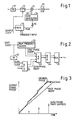
- Figure 1 illustrates a code correlation arrangement,
- Figure 2 illustrates a code frequency up-conversion arrangement,
- Figure 3 illustrates trajectories associated with the arrangement of Figure 2,
- Figure 4 illustrates phase trajectories for a modification to the arrangement of Figure 2,
- Figure 5 illustrates a simplified up-conversion arrangement, and
- Figure 6 illustrates waveforms associated with the arrangements of Figure 5.
- In the arrangement shown in Figure 1 an analogue signal modulated with coded information is passed through a low-
pass filter 10 and applied to asampling circuit 11. The sampled signal is then digitally multiplied with a synchronous code inmultiplier 12. The output ofmultiplier 12 is finally passed through a digital filter 13 the output of which consists of the correlation samples. The synchronous code applied tomultiplier 12 is produced by acode generator 14 which is clocked synchronously with the sample clock applied tocircuit 11. In order to maintain an accurate phase track of the incoming code phase the code generator must follow the incoming code phase. In other words, there must be provision for adjusting the phase of the locally produced code and therefore the phase of the code generator clock, relative to the sampling clock. This is achieved by generating phase samples from a numerically controlled oscillator (NCO) 15 clocked with the sampling clock. The generated phase samples are then quantised to one bit, is then used to clock the code generator in such a way that a clock will occur every sample time that the NCO phase passes 2π. It is evident that the sample clock must exceed or at least equal twice the highest code Doppler frequency if output clocks are not to be missed. For the convenience of the logic used by the applicants it was found necessary to include aninverter 16 to invert the most significant bit (MSB) before applying it to thecode generator 14. Finite NCO accumulator length will result in reduced frequency resolution.. The phase ramp will always be linear, implying that there will be no phase jitter. - There is one major problem, however, with the arrangement of Figure 1. It is difficult to build a multi-bit NCO running in excess of 20MHz using current CMOS technology. In a preferred embodiment of the invention, therefore, an up-conversion technique is used and this is illustrated in Figure 2.
- The basic up-converter arrangement utilises a fast clock applied to a
high frequency divider 20 near to the required output frequency. Thedivider 20 is implemented as a very fast counter producing an m-bit word in paralleloutput form. The sample rate of this ramp is thus approximately equal to the high frequency clock, e.g. the sample clock of Figure 1. To achieve a fine control of the ramp frequency the high frequency clock is also fed to adivider 21 to produce a slow clock which drives a slow running NCO 22. The output ofNCO 22, which is also an m-bit word, is added to the output ofdivider 20 in aparallel adder 23. The resultant m-bit sum is used to address aROM 24 which provides a digital representation of a sine wave. This is converted in a digital-to-analogue converter 25 to an analgoue sine wave which is then squared up to form the basic code generator clock. The associated phase trajectories are illustrated in Figure 3. It can be seen that the resulting phase errors are a function of the slow NCO frequency and the time between phase corrections compared to the fast divider clock. - The technique may be used to generate the sampled code clock by using some simplifications. The fast phase ramp may be generated by dividing the sample clock by 2. Alternate output samples of 0 or π will thus result. This represents a phase ramp of half the sample frequency. The ramp must therefore be slowed by subtracting an NCO phase ramp output. The resulting phase trajectory is shown in Figure 4. It can be seen that the maximum phase error is given by
φP = 9FS - F codemin) x TN x 2π-radians
where FS = sample frequency
Fcode = minimum code frequency
TN = slow NCO update time.
- The required code clock waveform may be obtained by truncating the phase sum to 1 bit and inverting. The addition may be performed simply by modulo one addition of the fast phase ramp to the slow NCO MSB. The resulting circuit is an exclusive OR gate followed by an inverter. The fast phase ramp may be generated by a D-type bistable connected to toggle. A possible circuit is shown in Figure 5.
- In the simplified arrangement of Figure 5 the fast sample clock is fed to the D-
type bistable 50 connected to function as a divide-by-two toggle. The fast clock is also fed to a divider.51 to produce a slow reference clock for the NCO 52. The output of the bistable 50 is summed with the most significant bit (MSB) of the NCO output in exclusive-OR gate 53 which is followed byinverter 54. It is assumed that the NCO is supplied with negative frequency input data. It must also be noted that the output would in practice need to be reclocked to remove glitches, The resultant waveforms are shown in Figure 6. It can be seen that the clock is delayed by one sample each time the NCO phase passes nπ.
Claims (4)
Applications Claiming Priority (2)
| Application Number | Priority Date | Filing Date | Title |
|---|---|---|---|
| GB8723855 | 1987-10-10 | ||
| GB8723855A GB2211051B (en) | 1987-10-10 | 1987-10-10 | Code correlation arrangement |
Publications (3)
| Publication Number | Publication Date |
|---|---|
| EP0312193A2 true EP0312193A2 (en) | 1989-04-19 |
| EP0312193A3 EP0312193A3 (en) | 1991-03-20 |
| EP0312193B1 EP0312193B1 (en) | 1994-06-08 |
Family
ID=10625139
Family Applications (1)
| Application Number | Title | Priority Date | Filing Date |
|---|---|---|---|
| EP88306672A Expired - Lifetime EP0312193B1 (en) | 1987-10-10 | 1988-07-20 | Code correlation arrangement |
Country Status (6)
| Country | Link |
|---|---|
| US (1) | US4910695A (en) |
| EP (1) | EP0312193B1 (en) |
| JP (1) | JP2713431B2 (en) |
| DE (1) | DE3850032T2 (en) |
| ES (1) | ES2064353T3 (en) |
| GB (1) | GB2211051B (en) |
Cited By (4)
| Publication number | Priority date | Publication date | Assignee | Title |
|---|---|---|---|---|
| US5101416A (en) * | 1990-11-28 | 1992-03-31 | Novatel Comunications Ltd. | Multi-channel digital receiver for global positioning system |
| US5390207A (en) * | 1990-11-28 | 1995-02-14 | Novatel Communications Ltd. | Pseudorandom noise ranging receiver which compensates for multipath distortion by dynamically adjusting the time delay spacing between early and late correlators |
| US5414729A (en) * | 1992-01-24 | 1995-05-09 | Novatel Communications Ltd. | Pseudorandom noise ranging receiver which compensates for multipath distortion by making use of multiple correlator time delay spacing |
| US5815539A (en) * | 1992-01-22 | 1998-09-29 | Trimble Navigation Limited | Signal timing synchronizer |
Families Citing this family (4)
| Publication number | Priority date | Publication date | Assignee | Title |
|---|---|---|---|---|
| US6493404B1 (en) * | 1999-03-01 | 2002-12-10 | Sharp Kabushiki Kaisha | Recycling integrator correlator |
| US6388600B1 (en) * | 2000-11-13 | 2002-05-14 | Trw Inc. | Asynchronous superconductor serial multiply-accumulator |
| US8260144B2 (en) * | 2008-03-12 | 2012-09-04 | Hypres Inc. | Digital radio frequency tranceiver system and method |
| JP6827878B2 (en) * | 2017-05-09 | 2021-02-10 | オリンパス株式会社 | Timing detector, timing control device, radio signal receiver and radio signal receiver for capsule endoscopy |
Citations (3)
| Publication number | Priority date | Publication date | Assignee | Title |
|---|---|---|---|---|
| US4484335A (en) * | 1982-10-14 | 1984-11-20 | E-Systems, Inc. | Method and apparatus for despreading a spread spectrum signal at baseband |
| US4530103A (en) * | 1983-08-22 | 1985-07-16 | E-Systems, Inc. | Method and apparatus for baseband tracking of a PN code sequence in a spread spectrum receiver |
| US4651154A (en) * | 1984-03-01 | 1987-03-17 | Standard Telephone And Cables Public Limited Company | Digital NAVSTAR receiver |
Family Cites Families (9)
| Publication number | Priority date | Publication date | Assignee | Title |
|---|---|---|---|---|
| US3510595A (en) * | 1967-08-11 | 1970-05-05 | Itt | Impulse autocorrelation function multiplex system |
| CH548607A (en) * | 1971-05-05 | 1974-04-30 | Hasler Ag | DEVICE FOR MEASURING THE RELATIVE SPEED AND / OR THE DISPLACEMENT TRAVEL OF A BODY PARALLEL TO A SURFACE. |
| US4112497A (en) * | 1977-03-29 | 1978-09-05 | Nasa | Digital demodulator-correlator |
| NL177552C (en) * | 1979-05-02 | 1985-10-01 | Nederlanden Staat | APPARATUS FOR DETERMINING THE PRESENCE OF EACH OF A NUMBER OF FIXED FREQUENCIES IN A SIGNAL USING A DIGITAL CORRELATION METHOD. |
| US4414676A (en) * | 1981-03-31 | 1983-11-08 | Motorola, Inc. | Signal synchronization system |
| DE3333714A1 (en) * | 1983-09-17 | 1985-04-04 | Standard Elektrik Lorenz Ag, 7000 Stuttgart | CIRCUIT ARRANGEMENT FOR FRAME AND PHASE SYNCHRONIZATION OF A RECEIVING SAMPLE CLOCK |
| US4706263A (en) * | 1983-11-07 | 1987-11-10 | Hughes Aircraft Company | Data communications receiver operable in highly stressed environments |
| US4689806A (en) * | 1983-11-07 | 1987-08-25 | Hughes Aircraft Company | Receiver mode control for acquiring and tracking a signal |
| US4627079A (en) * | 1983-11-07 | 1986-12-02 | Hughes Aircraft Company | Method and apparatus for acquiring and tracking a communications signal |
-
1987
- 1987-10-10 GB GB8723855A patent/GB2211051B/en not_active Expired - Lifetime
-
1988
- 1988-07-20 DE DE3850032T patent/DE3850032T2/en not_active Expired - Fee Related
- 1988-07-20 ES ES88306672T patent/ES2064353T3/en not_active Expired - Lifetime
- 1988-07-20 EP EP88306672A patent/EP0312193B1/en not_active Expired - Lifetime
- 1988-08-09 US US07/230,186 patent/US4910695A/en not_active Expired - Lifetime
- 1988-08-30 JP JP21620088A patent/JP2713431B2/en not_active Expired - Fee Related
Patent Citations (3)
| Publication number | Priority date | Publication date | Assignee | Title |
|---|---|---|---|---|
| US4484335A (en) * | 1982-10-14 | 1984-11-20 | E-Systems, Inc. | Method and apparatus for despreading a spread spectrum signal at baseband |
| US4530103A (en) * | 1983-08-22 | 1985-07-16 | E-Systems, Inc. | Method and apparatus for baseband tracking of a PN code sequence in a spread spectrum receiver |
| US4651154A (en) * | 1984-03-01 | 1987-03-17 | Standard Telephone And Cables Public Limited Company | Digital NAVSTAR receiver |
Cited By (6)
| Publication number | Priority date | Publication date | Assignee | Title |
|---|---|---|---|---|
| US5101416A (en) * | 1990-11-28 | 1992-03-31 | Novatel Comunications Ltd. | Multi-channel digital receiver for global positioning system |
| US5390207A (en) * | 1990-11-28 | 1995-02-14 | Novatel Communications Ltd. | Pseudorandom noise ranging receiver which compensates for multipath distortion by dynamically adjusting the time delay spacing between early and late correlators |
| US5495499A (en) * | 1990-11-28 | 1996-02-27 | Novatel Communications, Ltd. | Pseudorandom noise ranging receiver which compensates for multipath distortion by dynamically adjusting the time delay spacing between early and late correlators |
| US5809064A (en) * | 1990-11-28 | 1998-09-15 | Novatel, Inc. | Pseudorandom noise ranging receiver which compensates for multipath distortion by dynamically adjusting the time delay spacing between early and late correlators |
| US5815539A (en) * | 1992-01-22 | 1998-09-29 | Trimble Navigation Limited | Signal timing synchronizer |
| US5414729A (en) * | 1992-01-24 | 1995-05-09 | Novatel Communications Ltd. | Pseudorandom noise ranging receiver which compensates for multipath distortion by making use of multiple correlator time delay spacing |
Also Published As
| Publication number | Publication date |
|---|---|
| GB8723855D0 (en) | 1987-11-11 |
| JPH01103312A (en) | 1989-04-20 |
| US4910695A (en) | 1990-03-20 |
| DE3850032T2 (en) | 1994-09-29 |
| JP2713431B2 (en) | 1998-02-16 |
| GB2211051B (en) | 1991-07-10 |
| GB2211051A (en) | 1989-06-21 |
| ES2064353T3 (en) | 1995-02-01 |
| DE3850032D1 (en) | 1994-07-14 |
| EP0312193A3 (en) | 1991-03-20 |
| EP0312193B1 (en) | 1994-06-08 |
Similar Documents
| Publication | Publication Date | Title |
|---|---|---|
| US5790614A (en) | Synchronized clock using a non-pullable reference oscillator | |
| US6441655B1 (en) | Frequency division/multiplication with jitter minimization | |
| KR100447913B1 (en) | Playback apparatus and playback method | |
| JP3863522B2 (en) | Digital VCO, VCO circuit, PLL circuit, information recording apparatus, and synchronous clock signal generation method | |
| US7420426B2 (en) | Frequency modulated output clock from a digital phase locked loop | |
| US4910695A (en) | Code correlation arrangement | |
| US5546032A (en) | Clock signal regeneration method and apparatus | |
| CA1294334C (en) | Digital data separator | |
| US5987082A (en) | Playback apparatus and playback method | |
| EP0756744B1 (en) | Arrangement for reproducing n digital signals from n adjacent tracks on a record carrier | |
| EP0290851A2 (en) | Synchronizing clock signal generator | |
| KR960036465A (en) | 4-phase phase modulator | |
| US4914397A (en) | Digital frequency converter | |
| EP0493607B1 (en) | Clock regenerating circuit | |
| JPH07143000A (en) | Synchronous clock production method using controllable oscillator circuit | |
| US5726609A (en) | Pulse amplitude modulator using direct digital synthesizer | |
| US6317457B1 (en) | Pulse density modulator | |
| EP1241790B1 (en) | Full digital phase locked loop and circuitry for utilizing the same | |
| JP2733528B2 (en) | Partial pulse height reference frequency generator for phase locked loop | |
| CA1254270A (en) | Phase-locked loop | |
| JPS6058618B2 (en) | Bipolar code regeneration circuit | |
| JP3008659B2 (en) | Clock extraction circuit for CMI code signal | |
| KR100297854B1 (en) | D / A Converter for Oscillator Control of Phase-Locked Loop_ | |
| JPH0563746A (en) | Psk modulation circuit | |
| JPS637050A (en) | Fast timing extraction circuit |
Legal Events
| Date | Code | Title | Description |
|---|---|---|---|
| PUAI | Public reference made under article 153(3) epc to a published international application that has entered the european phase |
Free format text: ORIGINAL CODE: 0009012 |
|
| AK | Designated contracting states |
Kind code of ref document: A2 Designated state(s): DE ES FR IT |
|
| PUAL | Search report despatched |
Free format text: ORIGINAL CODE: 0009013 |
|
| AK | Designated contracting states |
Kind code of ref document: A3 Designated state(s): DE ES FR IT |
|
| 17P | Request for examination filed |
Effective date: 19910404 |
|
| 17Q | First examination report despatched |
Effective date: 19921208 |
|
| RAP1 | Party data changed (applicant data changed or rights of an application transferred) |
Owner name: NORTHERN TELECOM LIMITED |
|
| GRAA | (expected) grant |
Free format text: ORIGINAL CODE: 0009210 |
|
| AK | Designated contracting states |
Kind code of ref document: B1 Designated state(s): DE ES FR IT |
|
| ITF | It: translation for a ep patent filed |
Owner name: JACOBACCI CASETTA & PERANI S.P.A. |
|
| ET | Fr: translation filed | ||
| REF | Corresponds to: |
Ref document number: 3850032 Country of ref document: DE Date of ref document: 19940714 |
|
| REG | Reference to a national code |
Ref country code: ES Ref legal event code: FG2A Ref document number: 2064353 Country of ref document: ES Kind code of ref document: T3 |
|
| PLBE | No opposition filed within time limit |
Free format text: ORIGINAL CODE: 0009261 |
|
| STAA | Information on the status of an ep patent application or granted ep patent |
Free format text: STATUS: NO OPPOSITION FILED WITHIN TIME LIMIT |
|
| 26N | No opposition filed | ||
| REG | Reference to a national code |
Ref country code: ES Ref legal event code: PC2A |
|
| REG | Reference to a national code |
Ref country code: FR Ref legal event code: CD |
|
| PGFP | Annual fee paid to national office [announced via postgrant information from national office to epo] |
Ref country code: ES Payment date: 20050712 Year of fee payment: 18 |
|
| PGFP | Annual fee paid to national office [announced via postgrant information from national office to epo] |
Ref country code: FR Payment date: 20060705 Year of fee payment: 19 |
|
| PGFP | Annual fee paid to national office [announced via postgrant information from national office to epo] |
Ref country code: IT Payment date: 20060731 Year of fee payment: 19 Ref country code: DE Payment date: 20060731 Year of fee payment: 19 |
|
| PG25 | Lapsed in a contracting state [announced via postgrant information from national office to epo] |
Ref country code: DE Free format text: LAPSE BECAUSE OF NON-PAYMENT OF DUE FEES Effective date: 20080201 |
|
| REG | Reference to a national code |
Ref country code: FR Ref legal event code: ST Effective date: 20080331 |
|
| PG25 | Lapsed in a contracting state [announced via postgrant information from national office to epo] |
Ref country code: FR Free format text: LAPSE BECAUSE OF NON-PAYMENT OF DUE FEES Effective date: 20070731 |
|
| REG | Reference to a national code |
Ref country code: ES Ref legal event code: FD2A Effective date: 20070721 |
|
| PG25 | Lapsed in a contracting state [announced via postgrant information from national office to epo] |
Ref country code: ES Free format text: LAPSE BECAUSE OF NON-PAYMENT OF DUE FEES Effective date: 20070721 |
|
| PG25 | Lapsed in a contracting state [announced via postgrant information from national office to epo] |
Ref country code: IT Free format text: LAPSE BECAUSE OF NON-PAYMENT OF DUE FEES Effective date: 20070720 |