EP0313025A2 - Surface acoustic wave device - Google Patents
Surface acoustic wave device Download PDFInfo
- Publication number
- EP0313025A2 EP0313025A2 EP88117412A EP88117412A EP0313025A2 EP 0313025 A2 EP0313025 A2 EP 0313025A2 EP 88117412 A EP88117412 A EP 88117412A EP 88117412 A EP88117412 A EP 88117412A EP 0313025 A2 EP0313025 A2 EP 0313025A2
- Authority
- EP
- European Patent Office
- Prior art keywords
- acoustic wave
- surface acoustic
- degrees
- axis
- aluminum nitride
- Prior art date
- Legal status (The legal status is an assumption and is not a legal conclusion. Google has not performed a legal analysis and makes no representation as to the accuracy of the status listed.)
- Granted
Links
- 238000010897 surface acoustic wave method Methods 0.000 title claims abstract description 54
- PMHQVHHXPFUNSP-UHFFFAOYSA-M copper(1+);methylsulfanylmethane;bromide Chemical compound Br[Cu].CSC PMHQVHHXPFUNSP-UHFFFAOYSA-M 0.000 claims abstract description 56
- 239000013078 crystal Substances 0.000 claims abstract description 33
- 239000000758 substrate Substances 0.000 claims description 17
- 230000008878 coupling Effects 0.000 abstract description 28
- 238000010168 coupling process Methods 0.000 abstract description 28
- 238000005859 coupling reaction Methods 0.000 abstract description 28
- 238000000034 method Methods 0.000 description 12
- 238000010586 diagram Methods 0.000 description 7
- 238000004544 sputter deposition Methods 0.000 description 7
- 229910052594 sapphire Inorganic materials 0.000 description 4
- 239000010980 sapphire Substances 0.000 description 4
- 238000004364 calculation method Methods 0.000 description 3
- 238000004891 communication Methods 0.000 description 3
- 239000000463 material Substances 0.000 description 3
- XUIMIQQOPSSXEZ-UHFFFAOYSA-N Silicon Chemical compound [Si] XUIMIQQOPSSXEZ-UHFFFAOYSA-N 0.000 description 2
- 238000010276 construction Methods 0.000 description 2
- 239000011521 glass Substances 0.000 description 2
- 238000012545 processing Methods 0.000 description 2
- 239000010453 quartz Substances 0.000 description 2
- 238000011160 research Methods 0.000 description 2
- 229910052710 silicon Inorganic materials 0.000 description 2
- 239000010703 silicon Substances 0.000 description 2
- VYPSYNLAJGMNEJ-UHFFFAOYSA-N silicon dioxide Inorganic materials O=[Si]=O VYPSYNLAJGMNEJ-UHFFFAOYSA-N 0.000 description 2
- PIGFYZPCRLYGLF-UHFFFAOYSA-N Aluminum nitride Chemical compound [Al]#N PIGFYZPCRLYGLF-UHFFFAOYSA-N 0.000 description 1
- 229910052782 aluminium Inorganic materials 0.000 description 1
- PNEYBMLMFCGWSK-UHFFFAOYSA-N aluminium oxide Inorganic materials [O-2].[O-2].[O-2].[Al+3].[Al+3] PNEYBMLMFCGWSK-UHFFFAOYSA-N 0.000 description 1
- 238000006243 chemical reaction Methods 0.000 description 1
- 238000005229 chemical vapour deposition Methods 0.000 description 1
- 239000004020 conductor Substances 0.000 description 1
- 239000000498 cooling water Substances 0.000 description 1
- 229910052593 corundum Inorganic materials 0.000 description 1
- 238000011161 development Methods 0.000 description 1
- 239000010432 diamond Substances 0.000 description 1
- 229910003460 diamond Inorganic materials 0.000 description 1
- PSHMSSXLYVAENJ-UHFFFAOYSA-N dilithium;[oxido(oxoboranyloxy)boranyl]oxy-oxoboranyloxyborinate Chemical compound [Li+].[Li+].O=BOB([O-])OB([O-])OB=O PSHMSSXLYVAENJ-UHFFFAOYSA-N 0.000 description 1
- 230000000694 effects Effects 0.000 description 1
- 230000005284 excitation Effects 0.000 description 1
- 238000002474 experimental method Methods 0.000 description 1
- 238000010438 heat treatment Methods 0.000 description 1
- 238000001755 magnetron sputter deposition Methods 0.000 description 1
- 230000003287 optical effect Effects 0.000 description 1
- 238000007738 vacuum evaporation Methods 0.000 description 1
- 229910001845 yogo sapphire Inorganic materials 0.000 description 1
Images

Classifications
-
- H—ELECTRICITY
- H03—ELECTRONIC CIRCUITRY
- H03H—IMPEDANCE NETWORKS, e.g. RESONANT CIRCUITS; RESONATORS
- H03H9/00—Networks comprising electromechanical or electro-acoustic devices; Electromechanical resonators
- H03H9/02—Details
-
- H—ELECTRICITY
- H03—ELECTRONIC CIRCUITRY
- H03H—IMPEDANCE NETWORKS, e.g. RESONANT CIRCUITS; RESONATORS
- H03H9/00—Networks comprising electromechanical or electro-acoustic devices; Electromechanical resonators
- H03H9/02—Details
- H03H9/02535—Details of surface acoustic wave devices
- H03H9/02543—Characteristics of substrate, e.g. cutting angles
- H03H9/02574—Characteristics of substrate, e.g. cutting angles of combined substrates, multilayered substrates, piezoelectrical layers on not-piezoelectrical substrate
Definitions
- the present invention relates to surface acoustic wave devices wherein aluminum nitride is used as a piezoelectric material.
- Surface acoustic wave devices are small-sized and stable to temperature and to variations with time, can be adapted to give the desired filter characteristics by varying the configuration of comblike electrodes and therefore find wide application, for example, to IF filters for television receivers, IF filters for satellite broadcasting, RF converter osillators for VTRs, etc.
- surface acoustic wave devices be as great as possible in effective surface acoustic wave coupling coefficient K2 which represents the efficiency of conversion of electrical energy to surface acoustic wave energy.
- K2 represents the efficiency of conversion of electrical energy to surface acoustic wave energy.
- it has been proposed to give an improved coupling coefficient to surface acoustic wave devices employing a single crystal lithium tetraborate substrate by suitably selecting the direction of propagation of the wave (Unexamined Japanese Patent Publication SHO 59-4309).
- the device disclosed in the foregoing IEEE Transaction which comprises a single crystal film of (1120)[0001] AlN formed on a substrate of (0112)[0111] Al2O3 is as low as 0.8% in coupling coefficient K2.
- the device having a c-axis-oriented aluminum nitride film and disclosed in the above-mentioned Applied Physicas Letter has a very low coupling coefficient K2 of 0.12%.
- the main object of the present invention is to provide a surface acoustic wave device comprising a single crystal aluminum nitride film or a c-axis-oriented aluminum nitride film serving as a piezoelectric film and having a greater coupling coefficient than conventionally possible.
- the coupling coefficient of the device can be greatly increased by inclining the crystal orientation of the piezoelectric film with respect to a normal to the piezoelectric film, and further that with the surface acoustic wave device comprising a c-axis-oriented aluminum nitride film as a piezoelectric film, the coupling coefficient of the device can be greatly increased by inclining the direction of the c-axis orientation of the piezoelectric film with respect to a normal to the film.
- the present invention has been accomplished.
- ⁇ is set to 90 degrees as in the prior art, ⁇ to a desired angle, and ⁇ to an angle in the range of 30 to 150 degrees, preferably about 56 degrees or about 124 degrees. Conventionally, ⁇ is set to about 0 degree.
- the direction of c-axis orientation of the piezoelectric film is inclined within a plane containing the direction of propagation of a surface acoustic wave and perpendicular to the surface of the piezoelectric film at an angle in the range of about ⁇ 30 degrees to about ⁇ 150 degrees, preferably at about ⁇ 56 degrees or about ⁇ 124 degrees, with respect to a normal to the piezoelectric film.
- the angle of inclination is about 0 degree.
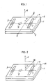
- Fig. 1 shows an example of surface acoustic wave device comprising a single crystal aluminum nitride film 2
- Fig. 2 shows an example of surface acoustic wave device comprising a c-axis-oriented aluminum nitride film 21.
- the single crystal or c-axis-oriented AlN film 2 or 21 has a thickness corresponding to several wavelengths of a surface acoustic wave (e.g., a thickness of 20 to 30 micrometers) and is formed on a substrate 1.
- a transmitting electrode 3 and a receiving electrode 4, each resembling a comb, are arranged as opposed to each other on the surface of the AlN film.
- the surface acoustic wave propagates from the transmitting electrode 3 toward the receiving electrode 4 in the direction of arrow 5.
- Fig. 5 is a diagram for illustrating how to express the direction of propagation of surface acoustic wave in the Euler angle notation.
- the diagram shows X-axis, Y-axis and Z-axis which represent the crystal axes crystallographically characteristic of the single crystal of aluminum nitride.
- the direction of propagation of the surface acoustic wave is represented by X1-axis, the direction of a normal to the surface of the piezoelectric film by X3-axis, and the direction perpendicular to X1-axis and to X3-axis by X2-axis.
- angles ⁇ , ⁇ and ⁇ are each in the range of 0 to 180 degrees and respectively include angles ( ⁇ + 180), ( ⁇ + 180) and ( ⁇ + 180) each involving a difference of 180 degrees in phase.
- the substrate 1 is made of sapphire, silicon single crystal, glass or quartz.
- the single crystal AlN film 2 is formed over the substrate 1.
- the coupling coefficient can be calculated by the known method disclosed, for example, in IEEE Transaction on Sonics and Ultrasonics, Vol. SU-15, No. 4, October 1968, pp. 209-217, "A Method for Estimating Optical Crystal Cuts and Propagation Direction for Excitation of Piezoelectric Surface Waves," and the Foundation of Japan Acoustics Society, material for l4th Technical Institute (April 1977), “Communication with Surface Acoustic Waves and Application to Signal Processing, " pp. 8-19.
- the coupling coefficient is determined by the numerical analysis of a model of surface acoustic wave device which comprises a basic piezoelectric equation which is prepared considering the anisotropy and piezoelectric characteristics of the AlN film, Newton's equation of motion, Maxell's electromagnetic equations, etc.
- This method is generally accepted as having high accuracy.
- We conducted the numerical analysis of the model of surface acoustic wave device with high precision using Newton's method, etc. to thereby calculate the surface acoustic wave propagation velocity Vm through the AlN film when the film is covered with a complete conductor and the propagation velocity Vf at the free surface.
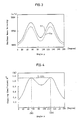
- Fig. 3 shows the propagation velocities Vm and Vf calculated for the device of Fig. 1 using the angle ⁇ as a parameter.
- the diagram indicates that both the propagation velocities Vm and Vf vary greatly with the angle ⁇ .
- Fig. 4 shows the coupling coefficient K2 calculated from the data of Fig. 3.
- the diagram reveals that the coupling coefficient curve has two peaks at varying angles ⁇ . The coefficient exceeds 0.8% over the ⁇ range of from about 30 degrees to about 150 degrees.
- the optimum values of angle ⁇ are about 56 degrees and about 124 degrees, at which the coupling coefficient K2 is 1.122.
- the single crystal AlN film has the crystal structure of hexagonal system, and X-axis is elastically equivalent to Y-axis, so that the coupling coefficient remains unchanged even when the angle ⁇ in the Euler angle notation changes over the range of 0 to 180 degrees. While the angle ⁇ is set to 90 degrees as in the prior art, we calculated the coupling coefficient in the same manner as above using the angle ⁇ as a parameter to find that the angle ⁇ is optimally 90 degrees.
- the wave propagation direction of the surface acoustic wave device having a single-crystal AlN film is expressed by ( ⁇ , ⁇ ,90) in the Euler angle notation, ⁇ of 0 to 180 degrees and ⁇ of 30 to 150 degrees, preferably ⁇ of about 56 degrees or about 124 degrees, assure the device of higher performance than theretofore possible.
- Such single crystal AlN film 2 can be formed by known CVD processes and sputtering process.
- MO-CVD metalorganic chemical vapor deposition
- Z-cut zirconium sputtering
- 45,90,90 AlN film is formed on a substrate as of sapphire single crystal, and the surface of the AlN film is thereafter ground to a specified angle with abrasive diamond grains.
- the substrate for forming the AlN film thereon is placed into a sputtering apparatus and inclined at a suitable angle with respect to the sputtering direction from the cathode to the anode, whereby an AlN film can be formed with Z-axis inclined according to the invention.
- the substrate 1 is made of sapphire, silicon single crystal, glass or quartz.
- the c-axis-oriented AlN film 21 is formed over the substrate 1. As illustrated, the film 21 has the direction W of c-axis orientation within a vertical plane containing the direction 7 of propagation of the surface acoustic wave and a normal 6 to the piezoelectric film.
- the coupling coefficient can be calculated by the same method as used for the single crystal aluminum nitride film.
- the model of surface acoustic wave device constructed for the calculation exhibits the same result as achieved by the use of the single crystal AlN film. Accordingly, the calculation of the coupling coefficient K2 affords the same result as shown in Fig. 4. More specifically, the coupling coefficient curve has two peaks at varying angles ⁇ , and the coefficient exceeds 0.8% when the angle ⁇ is in the range of from about 30 degrees to about 150 degrees.
- the optimum values of angle ⁇ are about 56 degrees and about 124 degrees, at which the coupling coefficient K2 is 1.122%.
- the device shown in Fig. 2 can be adapted to exhibit exceedingly higher performance than conventionally possible when the c-axis orientation direction W shown is set in the hatched angular ranges of Fig. 6, that is, when ⁇ is set to an angle in the range of +30 degrees to +150 degrees or in the range of -30 degrees to -150 degrees, more preferably when the angle ⁇ is about ⁇ 56 degrees or about ⁇ 124 degrees.
- the c-axis-oriented AlN film 21 can be prepared by the sputtering process or MO-CVD process.
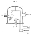
- Fig. 7 shows a sputtering vacuum evaporation apparatus.
- a bell jar 8 is in communication with a vacuum pump via an evacuation pipe 13 and connected to a gas supply pipe 14, and has Ar+N2 gas or Ar+NH3 gas enclosed therein.
- Arranged within the bell jar 8 are an anode electrode 9 of Al or Cu, and a cathode electrode 10 opposed thereto and provided with an Al target.
- An d.c. or high-frequency high-voltage power supply 12 is connected to the electrodes.
- the cathode electrode 10 is cooled with cooling water 11.
- a substrate 1 for forming an AlN film thereon faces the space between the cathode electrode 10 and the anode electrode 9 and is attached as inclined at a suitable angle to a holder 15.
- the holder 15 is equipped with a heater 16 for heating the substrate at 200 to 400° C.
- the angle at which the substrate 1 is to be positioned in place can be determined optimally by experiments.
- the power supply 12 when turned on, causes a discharge across the cathode electrode 10 and the anode electrode 9, consequently forming on the substrate 1 an AlN film with an inclined c-axis.
- the surface acoustic wave device of the present invention wherein the piezoelectric material is aluminum nitride has a higher coupling coefficient than the conventional devices.
- the substrate 1 can be omitted when an AlN panel is prepared which has a thickness (e.g. at least about 50 micrometers) to afford sufficient strength.
Abstract
Description
- The present invention relates to surface acoustic wave devices wherein aluminum nitride is used as a piezoelectric material.
- Surface acoustic wave devices are small-sized and stable to temperature and to variations with time, can be adapted to give the desired filter characteristics by varying the configuration of comblike electrodes and therefore find wide application, for example, to IF filters for television receivers, IF filters for satellite broadcasting, RF converter osillators for VTRs, etc.
- In recent years, especially, great efforts are directed to the development of high frequency surface acoustic wave devices for use in pocket pagers, mobile radio teleophones and the like. Attention has been focused on surface acoustic wave devices of this type which include a single crystal aluminum nitride film or a c-axis-oriented aluminum nitride film as a piezoelectric film assuring a high wave propagation velocity.
- Surface acoustic wave devices incorporating a single crystal aluminum nitride film are disclosed in IEEE Transaction on Sonics and Ultrasonics, Vol. SU-32, No. 5, September 1985, "Zero-Temperature-Coefficient SAW Devices on AlN Epitaxial Films." Further surface acoustic wave devices including a c-axis-oriented aluminum nitride film are disclosed in Applied Physics Letter, Vol. 36, No. 8, pp. 643-645, 15 April 1980, "Low-temperature growth of piezoelectric AlN film by rf reactive planar magnetron sputtering."
- It is desired that surface acoustic wave devices be as great as possible in effective surface acoustic wave coupling coefficient K² which represents the efficiency of conversion of electrical energy to surface acoustic wave energy. For example, it has been proposed to give an improved coupling coefficient to surface acoustic wave devices employing a single crystal lithium tetraborate substrate by suitably selecting the direction of propagation of the wave (Unexamined Japanese Patent Publication SHO 59-4309).
- However, full research has yet to be made on improvements in the coupling coefficient of surface acoustic wave devices employing an aluminum nitride (AlN) film. For example, the device disclosed in the foregoing IEEE Transaction, which comprises a single crystal film of (1120)[0001] AlN formed on a substrate of (0112)[0111] Al₂O₃ is as low as 0.8% in coupling coefficient K².
- The device having a c-axis-oriented aluminum nitride film and disclosed in the above-mentioned Applied Physicas Letter has a very low coupling coefficient K² of 0.12%.
- The main object of the present invention is to provide a surface acoustic wave device comprising a single crystal aluminum nitride film or a c-axis-oriented aluminum nitride film serving as a piezoelectric film and having a greater coupling coefficient than conventionally possible.
- To fulfill the above object, we have conducted research and theoretically found that with the surface acoustic wave device comprising a single crystal aluminum nitride film as a piezoelectric film, the coupling coefficient of the device can be greatly increased by inclining the crystal orientation of the piezoelectric film with respect to a normal to the piezoelectric film, and further that with the surface acoustic wave device comprising a c-axis-oriented aluminum nitride film as a piezoelectric film, the coupling coefficient of the device can be greatly increased by inclining the direction of the c-axis orientation of the piezoelectric film with respect to a normal to the film. Thus, the present invention has been accomplished.
- When the direction of propagation of a surface acoustic wave in the surface acoustic wave device having a single crystal aluminum nitride film is expressed as (λ,µ,ϑ) according to the Euler angle notation, ϑ is set to 90 degrees as in the prior art, λ to a desired angle, and µ to an angle in the range of 30 to 150 degrees, preferably about 56 degrees or about 124 degrees. Conventionally, µ is set to about 0 degree.
- With the surface acoustic wave device having a c-axis-oriented aluminum nitride film, the direction of c-axis orientation of the piezoelectric film is inclined within a plane containing the direction of propagation of a surface acoustic wave and perpendicular to the surface of the piezoelectric film at an angle in the range of about ±30 degrees to about ±150 degrees, preferably at about ±56 degrees or about ±124 degrees, with respect to a normal to the piezoelectric film. Conventionally, the angle of inclination is about 0 degree.
- Setting the angles λ, µ and ϑ of the single-crystal aluminum nitride film as stated above is equivalent in terms of elasticity to setting the direction of c-axis orientation of the c-axis-oriented aluminum nitride film as state above, and these two modes of setting produce the same effect with respect to the propagation of surface acoustic waves. This has been recognized by us and is also apparent from the analysis of the crystal structures.
- Consequently, both the devices theoretically have a coupling coefficient of up to a maximum of 1.122% which is a great improvement over a maximum of 0.8% conventionally available. The coupling coefficient was calculated by the numerical analysis of a model of surface acoustic wave device which is generally accepted as being highly reliable as will be described below, using a computer. Apparently, therefore, the theoretical value of coupling efficient given above has high accuracy.
-
- Fig. 1 is a perspective view of a surface acoustic wave device comprising a single crystal aluminum nitride film;
- Fig. 2 is a perspective view of a surface acoustic wave device comprising a c-axis oriented aluminum nitride film;
- Fig. 3 is a graph showing variations in surface acoustic wave propagation velocity;
- Fig. 4 is a graph showing variations in coupling coefficient;
- Fig. 5 is a diagram for illustrating the Euler angle notation;
- Fig. 6 is a diagram showing ranges of angles at which the direction of c-axis orientation is to be set; and
- Fig. 7 is a diagram schematically showing the construction of a sputtering apparatus.
- Fig. 1 shows an example of surface acoustic wave device comprising a single crystal aluminum nitride film 2, and Fig. 2 shows an example of surface acoustic wave device comprising a c-axis-oriented
aluminum nitride film 21. The single crystal or c-axis-oriented AlN film 2 or 21 has a thickness corresponding to several wavelengths of a surface acoustic wave (e.g., a thickness of 20 to 30 micrometers) and is formed on a substrate 1. A transmittingelectrode 3 and a receiving electrode 4, each resembling a comb, are arranged as opposed to each other on the surface of the AlN film. The surface acoustic wave propagates from the transmittingelectrode 3 toward the receiving electrode 4 in the direction ofarrow 5. - These devices will be described below in detail. (Embodiment of surface acoustic wave device having single crystal AlN film)
- Fig. 5 is a diagram for illustrating how to express the direction of propagation of surface acoustic wave in the Euler angle notation. The diagram shows X-axis, Y-axis and Z-axis which represent the crystal axes crystallographically characteristic of the single crystal of aluminum nitride. The direction of propagation of the surface acoustic wave is represented by X₁-axis, the direction of a normal to the surface of the piezoelectric film by X₃-axis, and the direction perpendicular to X₁-axis and to X₃-axis by X₂-axis.
- Suppose a line of intersection, A, of X₁-X₂ plane containing X₁-axis and X₂-axis with X-Y plane containing X-axis and Y-axis makes an angle of ϑ with X₁-axis, and the angle between the line of intersection A and X-axis is λ, and the angle between Z-axis and X₃-axis is µ. The direction of propagation of the surface acoustic wave is then expressed by (λ,µ,ϑ), and this system is referred to as the Euler notation.
- The angles λ,µ and ϑ are each in the range of 0 to 180 degrees and respectively include angles (λ + 180), (µ + 180) and (ϑ + 180) each involving a difference of 180 degrees in phase.
- With reference to Fig. 1, the substrate 1 is made of sapphire, silicon single crystal, glass or quartz. The single crystal AlN film 2 is formed over the substrate 1. The direction 7 of propagation of the surface acoustic wave through the film 2 is at right angles with X-axis of the crystal and represented by λ = 0 and ϑ = 90 in the Euler notation.
- In the course of accomplishing the present invention, we checked the device for variations in coupling coefficient when the angle µ between a normal 6 to the piezoelectric film and Z-axis of the crystal shown in Fig. 1 was altered from 0 degree to 180 degrees.
- The coupling coefficient can be calculated by the known method disclosed, for example, in IEEE Transaction on Sonics and Ultrasonics, Vol. SU-15, No. 4, October 1968, pp. 209-217, "A Method for Estimating Optical Crystal Cuts and Propagation Direction for Excitation of Piezoelectric Surface Waves," and the Foundation of Japan Acoustics Society, material for l4th Technical Institute (April 1977), "Communication with Surface Acoustic Waves and Application to Signal Processing, " pp. 8-19.
- According to this calculation method, the coupling coefficient is determined by the numerical analysis of a model of surface acoustic wave device which comprises a basic piezoelectric equation which is prepared considering the anisotropy and piezoelectric characteristics of the AlN film, Newton's equation of motion, Maxell's electromagnetic equations, etc. This method is generally accepted as having high accuracy. We conducted the numerical analysis of the model of surface acoustic wave device with high precision using Newton's method, etc. to thereby calculate the surface acoustic wave propagation velocity Vm through the AlN film when the film is covered with a complete conductor and the propagation velocity Vf at the free surface.
- Fig. 3 shows the propagation velocities Vm and Vf calculated for the device of Fig. 1 using the angle µ as a parameter. The diagram indicates that both the propagation velocities Vm and Vf vary greatly with the angle µ.
- As disclosed in the above-mentioned literature "Communication with Surface Acoustic Waves and Application to Signal Processing," p. 16, the coupling coefficient is calculated from the following equation.
K² = 2(Vf - Vm)/Vf - Fig. 4 shows the coupling coefficient K² calculated from the data of Fig. 3. The diagram reveals that the coupling coefficient curve has two peaks at varying angles µ. The coefficient exceeds 0.8% over the µ range of from about 30 degrees to about 150 degrees. The optimum values of angle µ are about 56 degrees and about 124 degrees, at which the coupling coefficient K² is 1.122.
- The single crystal AlN film has the crystal structure of hexagonal system, and X-axis is elastically equivalent to Y-axis, so that the coupling coefficient remains unchanged even when the angle λ in the Euler angle notation changes over the range of 0 to 180 degrees. While the angle ϑ is set to 90 degrees as in the prior art, we calculated the coupling coefficient in the same manner as above using the angle ϑ as a parameter to find that the angle ϑ is optimally 90 degrees.
- Accordingly, when the wave propagation direction of the surface acoustic wave device having a single-crystal AlN film is expressed by (λ,µ,90) in the Euler angle notation, λ of 0 to 180 degrees and µ of 30 to 150 degrees, preferably µ of about 56 degrees or about 124 degrees, assure the device of higher performance than theretofore possible.
- Such single crystal AlN film 2 can be formed by known CVD processes and sputtering process.
- When the MO-CVD (metalorganic chemical vapor deposition) process is resorted to which is predominantly used as a CVD process, (0,0,ϑ) (so-called Z-cut), or (45,90,90) AlN film is formed on a substrate as of sapphire single crystal, and the surface of the AlN film is thereafter ground to a specified angle with abrasive diamond grains. Alternatively when the sputtering process is employed, the substrate for forming the AlN film thereon is placed into a sputtering apparatus and inclined at a suitable angle with respect to the sputtering direction from the cathode to the anode, whereby an AlN film can be formed with Z-axis inclined according to the invention.
- With reference to Fig. 2, the substrate 1 is made of sapphire, silicon single crystal, glass or quartz. The c-axis-oriented
AlN film 21 is formed over the substrate 1. As illustrated, thefilm 21 has the direction W of c-axis orientation within a vertical plane containing the direction 7 of propagation of the surface acoustic wave and a normal 6 to the piezoelectric film. - In the course of accomplishing the present invention, we checked the device for variations in coupling coefficient when the angle µ between the c-axis orientation direction W and the normal 6 was altered from 0 degree to 180 degrees.
- The coupling coefficient can be calculated by the same method as used for the single crystal aluminum nitride film. The model of surface acoustic wave device constructed for the calculation exhibits the same result as achieved by the use of the single crystal AlN film. Accordingly, the calculation of the coupling coefficient K² affords the same result as shown in Fig. 4. More specifically, the coupling coefficient curve has two peaks at varying angles µ, and the coefficient exceeds 0.8% when the angle µ is in the range of from about 30 degrees to about 150 degrees. The optimum values of angle µ are about 56 degrees and about 124 degrees, at which the coupling coefficient K² is 1.122%.
- It is already known that with c-axis-oriented AlN films, a direction of propagation of the surface acoustic wave is elastically equivalent to a propagation direction opposite thereto and different therefrom by 180 degrees.
- Accordingly, the device shown in Fig. 2 can be adapted to exhibit exceedingly higher performance than conventionally possible when the c-axis orientation direction W shown is set in the hatched angular ranges of Fig. 6, that is, when µ is set to an angle in the range of +30 degrees to +150 degrees or in the range of -30 degrees to -150 degrees, more preferably when the angle µ is about ± 56 degrees or about ±124 degrees.
- Like the film already described, the c-axis-oriented
AlN film 21 can be prepared by the sputtering process or MO-CVD process. - Fig. 7 shows a sputtering vacuum evaporation apparatus. A bell jar 8 is in communication with a vacuum pump via an
evacuation pipe 13 and connected to a gas supply pipe 14, and has Ar⁺N₂ gas or Ar⁺NH₃ gas enclosed therein. Arranged within the bell jar 8 are an anode electrode 9 of Al or Cu, and a cathode electrode 10 opposed thereto and provided with an Al target. An d.c. or high-frequency high-voltage power supply 12 is connected to the electrodes. The cathode electrode 10 is cooled with cooling water 11. - A substrate 1 for forming an AlN film thereon faces the space between the cathode electrode 10 and the anode electrode 9 and is attached as inclined at a suitable angle to a
holder 15. Theholder 15 is equipped with aheater 16 for heating the substrate at 200 to 400° C. The angle at which the substrate 1 is to be positioned in place can be determined optimally by experiments. - The
power supply 12, when turned on, causes a discharge across the cathode electrode 10 and the anode electrode 9, consequently forming on the substrate 1 an AlN film with an inclined c-axis. - As described above, the surface acoustic wave device of the present invention wherein the piezoelectric material is aluminum nitride has a higher coupling coefficient than the conventional devices.
- The device of the present invention is not limited to the foregoing embodiments in construction but can be modified variously by one skilled in the art without departing from the scope of the invention as defined in the appended claims.
- For example, although the
AlN film 2 or 21 is formed on the surface of the substrate 1 of sapphire or the like according to the foregoing embodiments, the substrate 1 can be omitted when an AlN panel is prepared which has a thickness (e.g. at least about 50 micrometers) to afford sufficient strength.
Claims (8)
Applications Claiming Priority (4)
| Application Number | Priority Date | Filing Date | Title |
|---|---|---|---|
| JP264736/87 | 1987-10-19 | ||
| JP62264736A JPH01106514A (en) | 1987-10-19 | 1987-10-19 | Surface acoustic wave element |
| JP62283969A JPH01125012A (en) | 1987-11-09 | 1987-11-09 | Surface acoustic wave element |
| JP283969/87 | 1987-11-09 |
Publications (3)
| Publication Number | Publication Date |
|---|---|
| EP0313025A2 true EP0313025A2 (en) | 1989-04-26 |
| EP0313025A3 EP0313025A3 (en) | 1990-04-04 |
| EP0313025B1 EP0313025B1 (en) | 1994-02-16 |
Family
ID=26546643
Family Applications (1)
| Application Number | Title | Priority Date | Filing Date |
|---|---|---|---|
| EP88117412A Expired - Lifetime EP0313025B1 (en) | 1987-10-19 | 1988-10-19 | Surface acoustic wave device |
Country Status (4)
| Country | Link |
|---|---|
| US (1) | US4868444A (en) |
| EP (1) | EP0313025B1 (en) |
| KR (1) | KR970004619B1 (en) |
| DE (1) | DE3887813T2 (en) |
Cited By (5)
| Publication number | Priority date | Publication date | Assignee | Title |
|---|---|---|---|---|
| EP0392449A1 (en) * | 1989-04-11 | 1990-10-17 | SANYO ELECTRIC Co., Ltd. | Surface acoustic wave device |
| EP0616426A1 (en) * | 1993-03-15 | 1994-09-21 | Matsushita Electric Industrial Co., Ltd. | Surface acoustic wave device having a lamination structure |
| AT401837B (en) * | 1993-03-04 | 1996-12-27 | Avl Verbrennungskraft Messtech | PIEZOELECTRIC CRYSTAL ELEMENT |
| EP0833446A2 (en) * | 1996-09-27 | 1998-04-01 | Ngk Insulators, Ltd. | Surface acoustic wave device, substrate therefor, and method of manufacturing the substrate |
| WO1998051008A1 (en) * | 1997-05-09 | 1998-11-12 | Kobe Steel Usa Inc. | Surface acoustic wave devices containing isolated interdigitated electrodes |
Families Citing this family (8)
| Publication number | Priority date | Publication date | Assignee | Title |
|---|---|---|---|---|
| JPH0314305A (en) * | 1989-06-13 | 1991-01-23 | Murata Mfg Co Ltd | Manufacture of surface acoustic wave device |
| JPH05259802A (en) * | 1992-03-16 | 1993-10-08 | Japan Energy Corp | Surface acoustic wave device |
| JPH06326548A (en) * | 1993-05-14 | 1994-11-25 | Kobe Steel Ltd | Surface acoustic wave element using highly orientational diamond thin film |
| US5498920A (en) * | 1993-05-18 | 1996-03-12 | Sanyo Electric Co., Ltd. | Acoustic wave device and process for producing same |
| DE69526748T2 (en) * | 1994-02-25 | 2002-09-05 | Sumitomo Electric Industries | Substrate for aluminum nitride thin film and process for its manufacture |
| US5576589A (en) * | 1994-10-13 | 1996-11-19 | Kobe Steel Usa, Inc. | Diamond surface acoustic wave devices |
| US10291203B2 (en) * | 2016-07-12 | 2019-05-14 | Murata Manufacturing Co., Ltd. | Piezoelectric MEMS resonator with a high quality factor |
| US10483943B2 (en) * | 2017-06-27 | 2019-11-19 | Globalfoundries Inc. | Artificially oriented piezoelectric film for integrated filters |
Citations (1)
| Publication number | Priority date | Publication date | Assignee | Title |
|---|---|---|---|---|
| GB2181917A (en) * | 1982-03-11 | 1987-04-29 | Nobuo Mikoshiba | Surface acoustic wave device |
Family Cites Families (3)
| Publication number | Priority date | Publication date | Assignee | Title |
|---|---|---|---|---|
| US4511816A (en) * | 1982-03-11 | 1985-04-16 | Nobuo Mikoshiba | Surface acoustic wave device using an elastic substrate and an aluminum nitride piezoelectric film |
| JPS59231911A (en) * | 1983-06-14 | 1984-12-26 | Clarion Co Ltd | Surface acoustic wave element |
| JPS60119114A (en) * | 1983-11-30 | 1985-06-26 | Murata Mfg Co Ltd | Surface wave device |
-
1988
- 1988-10-18 KR KR1019880013563A patent/KR970004619B1/en not_active IP Right Cessation
- 1988-10-18 US US07/259,557 patent/US4868444A/en not_active Expired - Lifetime
- 1988-10-19 DE DE3887813T patent/DE3887813T2/en not_active Expired - Fee Related
- 1988-10-19 EP EP88117412A patent/EP0313025B1/en not_active Expired - Lifetime
Patent Citations (1)
| Publication number | Priority date | Publication date | Assignee | Title |
|---|---|---|---|---|
| GB2181917A (en) * | 1982-03-11 | 1987-04-29 | Nobuo Mikoshiba | Surface acoustic wave device |
Non-Patent Citations (1)
| Title |
|---|
| ELECTRONICS AND COMMUNICATIONS IN JAPAN/Part II:ELECTRONICS, vol. 69, no. 5, 1986, pages 28-37, Scripta Technica, Inc., New York, NY., US; M. MATSUOKA et al.: "High rate preparation of C-Axis oriented AIN films by reactive sputtering" * |
Cited By (11)
| Publication number | Priority date | Publication date | Assignee | Title |
|---|---|---|---|---|
| EP0392449A1 (en) * | 1989-04-11 | 1990-10-17 | SANYO ELECTRIC Co., Ltd. | Surface acoustic wave device |
| US5059847A (en) * | 1989-04-11 | 1991-10-22 | Sanyo Electric Co., Ltd. | Surface acoustic wave device |
| AT401837B (en) * | 1993-03-04 | 1996-12-27 | Avl Verbrennungskraft Messtech | PIEZOELECTRIC CRYSTAL ELEMENT |
| EP0616426A1 (en) * | 1993-03-15 | 1994-09-21 | Matsushita Electric Industrial Co., Ltd. | Surface acoustic wave device having a lamination structure |
| US5446330A (en) * | 1993-03-15 | 1995-08-29 | Matsushita Electric Industrial Co., Ltd. | Surface acoustic wave device having a lamination structure |
| EP0833446A2 (en) * | 1996-09-27 | 1998-04-01 | Ngk Insulators, Ltd. | Surface acoustic wave device, substrate therefor, and method of manufacturing the substrate |
| EP0833446A3 (en) * | 1996-09-27 | 2000-01-26 | Ngk Insulators, Ltd. | Surface acoustic wave device, substrate therefor, and method of manufacturing the substrate |
| US6183555B1 (en) | 1996-09-27 | 2001-02-06 | Ngk Insulators, Ltd. | Surface acoustic wave device, substrate therefor, and method of manufacturing the substrate |
| WO1998051008A1 (en) * | 1997-05-09 | 1998-11-12 | Kobe Steel Usa Inc. | Surface acoustic wave devices containing isolated interdigitated electrodes |
| WO1998051009A1 (en) * | 1997-05-09 | 1998-11-12 | Kobe Steel Usa Inc. | SURFACE ACOUSTIC WAVE AND BULK ACOUSTIC WAVE DEVICES USING A Zn(1-x) YxO PIEZOELECTRIC LAYER DEVICE |
| US6127768A (en) * | 1997-05-09 | 2000-10-03 | Kobe Steel Usa, Inc. | Surface acoustic wave and bulk acoustic wave devices using a Zn.sub.(1-X) Yx O piezoelectric layer device |
Also Published As
| Publication number | Publication date |
|---|---|
| DE3887813D1 (en) | 1994-03-24 |
| KR890007443A (en) | 1989-06-19 |
| EP0313025B1 (en) | 1994-02-16 |
| DE3887813T2 (en) | 1994-06-23 |
| US4868444A (en) | 1989-09-19 |
| EP0313025A3 (en) | 1990-04-04 |
| KR970004619B1 (en) | 1997-03-29 |
Similar Documents
| Publication | Publication Date | Title |
|---|---|---|
| EP0313025B1 (en) | Surface acoustic wave device | |
| US6510597B2 (en) | Surface acoustic wave device and method of manufacturing the same | |
| EP0392449B1 (en) | Surface acoustic wave device | |
| US5917265A (en) | Optimal cut for saw devices on langasite | |
| EP0534355B1 (en) | Method of manufacturing a surface acoustic wave device | |
| EP0556811B1 (en) | Surface acoustic wave device | |
| Shiosaki et al. | Piezoelectric thin films for SAW applications | |
| US5081389A (en) | Crystal cut angles for lithium tantalate crystal for novel surface acoustic wave devices | |
| Kadota et al. | Characteristics of zinc oxide films on glass substrates deposited by RF-mode electron cyclotron resonance sputtering system | |
| US6054794A (en) | Optimal cut for wave propagation surface on langanite substrate | |
| US4670680A (en) | Doubly rotated orientations of cut angles for quartz crystal for novel surface acoustic wave devices | |
| US6097131A (en) | Optimal cut for SAW devices on langatate | |
| EP0534252B1 (en) | Surface acoustic wave device | |
| US5498920A (en) | Acoustic wave device and process for producing same | |
| Hickernell et al. | Surface‐elastic‐wave properties of dc‐triode‐sputtered zinc oxide films | |
| JPH09238039A (en) | Element including surface skimming bulk wave substrate and its method | |
| EP0955726B1 (en) | Surface acoustic wave apparatus | |
| US4511817A (en) | Temperature compensated orientation of berlinite for surface acoustic wave devices | |
| US4707631A (en) | Isotropic acoustic wave substrate | |
| JPH0548642B2 (en) | ||
| EP0144544B1 (en) | Temperature compensated orientation of berlinite for surface acoustic wave devices | |
| JPH1131942A (en) | Surface acoustic wave module element and its production | |
| Takeda et al. | High coupling and high velocity surface acoustic waves using ac‐axis oriented ZnO film on translucent Al2O3 ceramics | |
| JPH01125012A (en) | Surface acoustic wave element | |
| Dieulesaint et al. | Properties of piezoelectric Selenium and Selenium layers |
Legal Events
| Date | Code | Title | Description |
|---|---|---|---|
| PUAI | Public reference made under article 153(3) epc to a published international application that has entered the european phase |
Free format text: ORIGINAL CODE: 0009012 |
|
| AK | Designated contracting states |
Kind code of ref document: A2 Designated state(s): DE FR GB |
|
| PUAL | Search report despatched |
Free format text: ORIGINAL CODE: 0009013 |
|
| AK | Designated contracting states |
Kind code of ref document: A3 Designated state(s): DE FR GB |
|
| 17P | Request for examination filed |
Effective date: 19900910 |
|
| 17Q | First examination report despatched |
Effective date: 19920728 |
|
| GRAA | (expected) grant |
Free format text: ORIGINAL CODE: 0009210 |
|
| AK | Designated contracting states |
Kind code of ref document: B1 Designated state(s): DE FR GB |
|
| ET | Fr: translation filed | ||
| REF | Corresponds to: |
Ref document number: 3887813 Country of ref document: DE Date of ref document: 19940324 |
|
| PLBE | No opposition filed within time limit |
Free format text: ORIGINAL CODE: 0009261 |
|
| STAA | Information on the status of an ep patent application or granted ep patent |
Free format text: STATUS: NO OPPOSITION FILED WITHIN TIME LIMIT |
|
| 26N | No opposition filed | ||
| REG | Reference to a national code |
Ref country code: GB Ref legal event code: IF02 |
|
| PGFP | Annual fee paid to national office [announced via postgrant information from national office to epo] |
Ref country code: FR Payment date: 20041008 Year of fee payment: 17 |
|
| PGFP | Annual fee paid to national office [announced via postgrant information from national office to epo] |
Ref country code: GB Payment date: 20041013 Year of fee payment: 17 |
|
| PGFP | Annual fee paid to national office [announced via postgrant information from national office to epo] |
Ref country code: DE Payment date: 20041014 Year of fee payment: 17 |
|
| PG25 | Lapsed in a contracting state [announced via postgrant information from national office to epo] |
Ref country code: GB Free format text: LAPSE BECAUSE OF NON-PAYMENT OF DUE FEES Effective date: 20051019 |
|
| PG25 | Lapsed in a contracting state [announced via postgrant information from national office to epo] |
Ref country code: DE Free format text: LAPSE BECAUSE OF NON-PAYMENT OF DUE FEES Effective date: 20060503 |
|
| GBPC | Gb: european patent ceased through non-payment of renewal fee |
Effective date: 20051019 |
|
| PG25 | Lapsed in a contracting state [announced via postgrant information from national office to epo] |
Ref country code: FR Free format text: LAPSE BECAUSE OF NON-PAYMENT OF DUE FEES Effective date: 20060630 |
|
| REG | Reference to a national code |
Ref country code: FR Ref legal event code: ST Effective date: 20060630 |