EP0329285B1 - Output buffer - Google Patents
Output buffer Download PDFInfo
- Publication number
- EP0329285B1 EP0329285B1 EP89300583A EP89300583A EP0329285B1 EP 0329285 B1 EP0329285 B1 EP 0329285B1 EP 89300583 A EP89300583 A EP 89300583A EP 89300583 A EP89300583 A EP 89300583A EP 0329285 B1 EP0329285 B1 EP 0329285B1
- Authority
- EP
- European Patent Office
- Prior art keywords
- pull
- output
- transistor
- buffer
- input
- Prior art date
- Legal status (The legal status is an assumption and is not a legal conclusion. Google has not performed a legal analysis and makes no representation as to the accuracy of the status listed.)
- Expired - Lifetime
Links
Images

Classifications
-
- H—ELECTRICITY
- H03—ELECTRONIC CIRCUITRY
- H03K—PULSE TECHNIQUE
- H03K19/00—Logic circuits, i.e. having at least two inputs acting on one output; Inverting circuits
- H03K19/003—Modifications for increasing the reliability for protection
- H03K19/00346—Modifications for eliminating interference or parasitic voltages or currents
- H03K19/00361—Modifications for eliminating interference or parasitic voltages or currents in field effect transistor circuits
-
- H—ELECTRICITY
- H03—ELECTRONIC CIRCUITRY
- H03K—PULSE TECHNIQUE
- H03K19/00—Logic circuits, i.e. having at least two inputs acting on one output; Inverting circuits
- H03K19/003—Modifications for increasing the reliability for protection
- H03K19/00346—Modifications for eliminating interference or parasitic voltages or currents
- H03K19/00353—Modifications for eliminating interference or parasitic voltages or currents in bipolar transistor circuits
-
- H—ELECTRICITY
- H03—ELECTRONIC CIRCUITRY
- H03K—PULSE TECHNIQUE
- H03K19/00—Logic circuits, i.e. having at least two inputs acting on one output; Inverting circuits
- H03K19/01—Modifications for accelerating switching
- H03K19/013—Modifications for accelerating switching in bipolar transistor circuits
- H03K19/0136—Modifications for accelerating switching in bipolar transistor circuits by means of a pull-up or down element
-
- H—ELECTRICITY
- H03—ELECTRONIC CIRCUITRY
- H03K—PULSE TECHNIQUE
- H03K19/00—Logic circuits, i.e. having at least two inputs acting on one output; Inverting circuits
- H03K19/01—Modifications for accelerating switching
- H03K19/017—Modifications for accelerating switching in field-effect transistor circuits
- H03K19/01707—Modifications for accelerating switching in field-effect transistor circuits in asynchronous circuits
- H03K19/01721—Modifications for accelerating switching in field-effect transistor circuits in asynchronous circuits by means of a pull-up or down element
Definitions
- This invention relates generally to integrated circuits and more particularly, it relates to an output buffer such as a full-level, fast CMOS output buffer for driving widely varying capacitive and inductive loads without significant output ringing.
- output buffer is an important component for this interface function.
- the output buffer provides, when enabled, an output signal which is a function of a data input signal received from other logic circuitry of the integrated circuit.
- Output buffer circuits typically use a pull-up field-effect transistor (FET) and a pull-down field-effect transistor connected to an output node. Depending upon the state of data input signal and an enable signal, either the pull-up or pull-down field-effect transistor is quickly turned on and the other one of them is turned off.
- FET field-effect transistor
- Such prior art output buffer circuits generally have the output node connected to an external pin of an integrated circuit for driving other circuitry on other integrated circuits which may have widely varying capacitive and inductive loading effects.
- oscillation or inductive ringing appears on the output node of the buffer circuit as a function of the energy remaining in the parasitic interconnect inductances following the output transition and the impedance of the output driver in a circuit that includes the output loads, buffer drivers, and the ground loop.
- United States Patent Specification US-A-4,638,187 discloses a CMOS output buffer having field effect transistor pull-up and pull-down circuits which distribute switching current spikes over time.
- the pull-up circuit includes an P-channel FET and an N-channel FET connected in parallel between an output terminal and supply terminal V DD , with an inverter connected between the gates of the N-channel and P-channel FETs to provide the proper phase for the P-channel FETs as well as delaying turn-on of the P-channel FET with respect to the turn on the N-channel FET, and the N-channel FET shuts off when the output voltage reaches a certain potential.
- the pull down circuit includes a pair of N-channel FETs connected in parallel between the output terminal and ground, and a delay resistance connected between their gates so that turn-on of one of the N-channel FETs is delayed with respect to the other.
- the output buffer circuit to be described includes a pull-up circuit formed of a first pull-up transistor and a second pull-up transistor and a pull-down circuit formed of a first pull-down transistor and a second pull-down transistor.
- the reduction in the inductive ringing at the output node is achieved by increasing the driving transistors' equivalent impedance at the output node towards the end of either a low-to-high or high-to-low transition.
- the present invention provides an output buffer for driving a load the capacitance and inductance of which may vary widely, with a reduction of inductive ringing at an output node thereof, comprising: a pull-up circuit responsive to a first control signal, including a first pull-up transistor comprising a first N-channel transistor having its drain connected to a first supply voltage node and its source connected to said output node, and a second pull-up transistor comprising a first P-channel transistor having its source connected to said first supply potential, and its drain connected to said output node, and first and second inverters connected in series between a first control signal input to the buffer and the gate of said first N-channel transistor to control conduction thereof; a pull-down circuit responsive to a second control signal, including a first pull-down transistor comprising a second P-channel transistor having its source connected to said output node and its drain connected to a second supply potential, and a second pull-down transistor comprising a second N-channel transistor having its drain connected to said output node and its source connected
- an output buffer for driving a load the capacitance and inductance of which may vary widely, with a reduction of inductive ringing at an output node thereof, comprising: a pull-up circuit responsive to a first control signal, including a first pull-up transistor comprising a first NPN transistor having its collector connected to a first supply voltage node and its emitter connected to said output node, and a second pull-up transistor comprising a first PNP transistor having its emitter connected to said first supply potential, and its collector connected to said output node, and first and second inverters connected in series between a first control signal input to the buffer and the base of said first NPN transistor to control conduction thereof; a pull-down circuit responsive to a second control signal, including a first pull-down transistor comprising a second PNP transistor having its emitter connected to said output node and its collector connected to a second supply potential, and a second pull-down transistor comprising a second NPN transistor having its collector connected to said output node
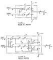
- FIG. 1 a schematic circuit diagram of a prior art output buffer circuit 10 formed of a P-channel pull-up field-effect transistor (FET) P1 and an N-channel pull-down FET N1.
- the buffer circuit 10 provides an output signal at an output node A in response to a data input signal INPUT received at a data input node D and an enable signal ENABLE received at enable input node E.
- the buffer circuit 10 includes a NOR logic gate 12, a NAND logic gate 14, and inverters 16, 18 and 20.
- the output node A of the buffer circuit 10 is used to drive a varying capacitive and inductive load represented by impedance CAP. Further, the output node A is typically connected to an internal node 22 via a lead connection 24 having parasitic inductance L.
- the NOR logic gate 12 receives the data input signal INPUT on line 26 on its one input and the enable signal ENABLE on line 28 via the inverter 16 on its other input.
- the output of the NOR logic gate 12 on line 30 is supplied to the gate of the P-channel pull-up transistor P1 via the inverter 18.
- the transistor P1 has its source connected via a lead line having parasitic inductance L(VCC) to a supply potential VCC, which is typically +5.0 volts, and has its drain connected via the lead connection 24 with the parasitic inductance L to the output node A.
- the NAND logic gate 14 receives the same data input signal INPUT on line 26 on its one input and the same enable signal ENABLE on the line 28 on its other input.
- the output of the NAND gate 14 on line 34 is applied to the gate of the N-channel pull-down transistor N1 via the inverter 20.
- the transistor N1 has its source connected via a lead line having parasitic inductance L(VSS)to a ground potential and its drain also connected via the lead connection 24 to the output node A.
- the magnitude of the voltage at the output node A in the buffer circuit 10 is dependent upon the capacitive and inductive load or impedance CAP being driven and the parasitic inductances.
- Such rapid switching on of the pull-up or pull-down field-effect transistors causes sudden surges of current commonly known as current spikes. These current spikes will flow through the parasitic inductances in the lead connections so as to cause oscillations or inductive ringing at the output node A of the buffer circuit 10.
- FIG 2 there is shown an output buffer circuit 10a of the present invention which represents an improvement over the buffer circuit 10 of Figure 1.
- the buffer circuit 10a provides the capability of driving quickly output loads that vary widely in capacitance and inductance to full-levels but yet reduces significantly the inductive ringing in the output signal due to the pull-up and pull-down output drivers switching states.
- the output buffer circuit 10a provides an output signal at an output node B in response to a data input signal INPUT received at data input node F and an enable signal ENABLE received at enable input node G.
- the output buffer circuit 10a includes a NOR logic gate 36, a NAND logic gate 40, an inverter 44, a pull-up circuit 37, and a pull-down circuit 39.
- the pull-up circuit 37 includes inverters 46, 48; a first pull-up N-channel transistor N2; a NAND logic gate 42; and a second pull-up P-channel transistor P2.
- the pull-down circuit 39 includes inverters 50, 52; a first pull-down P-channel transistor P3; a NOR logic gate 38; and a second pull-down N-channel transistor N3.
- the output node B is connected to an internal node C via a lead connection 56 having parasitic inductance L.
- a widely varying capacitive and inductive load represented by impedance CAP is connected between the output node B and a ground potential.
- the NOR logic gate 36 receives the data input signal INPUT on line 58 on its one input and the enable signal ENABLE on line 60 via the inverter 44 on its other input.
- the output of the NOR gate 36 provides a first control signal and is inverted twice by the inverters 46, 48.
- the output of the inverter 48 is connected to the gate of the first pull-up transistor N2 and to one input of the NAND gate 42.
- the output of the NOR logic gate 36 is also connected to the other input of the NAND gate 42.
- the first pull-up transistor N2 has its drain connected via a lead line having parasitic inductance L(VCC) to a supply potential VCC and its source connected via a lead line having parasitic inductance L to the output node B.
- the output of the NAND gate 42 is connected to the gate of the second pull-up transistor P2.
- the second pull-up transistor P2 has its source connected also via the line with the parasitic inductance L(VCC) to the supply potential VCC and its drain connected via the line 56 to the output node B.
- the NAND logic gate 40 receives the same data input signal INPUT on line 58 on its one input and the same enable signal ENABLE on line 60 on its other input.
- the output of the NAND logic gate 40 provides a second control signal and is inverted twice by the inverters 50, 52.
- the output of the inverter 52 is connected to the gate of the first pull-down transistor P3 and to one input of the NOR gate 38.
- the output of the NAND gate 40 is also connected to the other input of the NOR gate 38.
- the first pull-down transistor P3 has its source connected via the line 56 to the output node B and its drain connected via the line with the parasitic inductance L(VSS) to the ground potential.
- the output of the NOR gate 38 is connected to the gate of the second pull-down transistor N3.
- the second pull-down transistor N3 has its drain connected also via the line 56 to the output node B and its source connected via the line with the parasitic inductance L(VSS) to the ground potential.
- the pull-up action is started initially by the turning on of the first pull-up transistor N2 followed quickly by the turning on of the second pull-up transistor P2.
- the transistors N2 and P2 supply current to drive the output node B from the low logic state to the high logic state.
- the voltage on node C leads the voltage on node B as current in parasitic interconnect inductance L builds up to a peak in the early part of the transition due to both transistors N2 and P2 having turned on with the maximum drain-to-source voltage.
- the current in inductance L decreases causing the voltage on node C to lag the voltage on the output node B.
- the first pull-up transistor N2 turns off increasing the output impedance.
- This increased output impedance has two effects: (1) the drive current in the interconnect inductance L is reduced earlier in the transition and more quickly than in an equivalent prior art output buffer dissipating the energy stored in the interconnect inductance and causing the voltage across inductance L to increase temporarily; and (2) the low-to-high transition rate of node C is reduced with a subsequent damped response.
- the resulting response of output node B reflects the dampened response of node C with an offset voltage in the parasitic inductance L that accelerates the completion of the output transition.
- the parasitic inductance L is sufficiently large, there is one further effect that reduces the energy stored in the parasitic interconnect inductance and thus reduces the output ringing.
- the voltage on node C leads that on node B approaching a threshold below the supply voltage VCC causing the first pull-up transistor N2 to turn off. This reduces the drive current causing the voltage on the node C to quickly lag that on the output node B and fall once again turning on the transistor N2. Since the pull-up transistor N2 is off in part of the early stages of the output transition, the drive current level reaches in the interconnect inductance L is reduced relative to that reached by a comparable prior art output buffer. The remainder of the transition continues as previously described and is illustrated in Figure 3.
- the pull-down action is started initially by the turning on of the first pull-down transistor P3 followed by the turning on of the second pull-down transistor N3.
- the transistors P3 and N3 supply current to drive the output node B from the high logic state to the low logic state.
- the voltage on node C leads the voltage on node B as current in inductance L builds up to a peak in the early part of the transition due to both transistors P3 and N3 having turned on with the maximum drain-to-source voltage.
- the current in inductance L decreases causing the voltage on node C to lag the voltage on the output node B.
- the first pull-down transistor P3 turns off increasing the output impedance.
- This increased output impedance has two effects: (1) the drive current in the parasitic interconnect inductance L is reduced earlier in the transition and more quickly than in an equivalent conventional output buffer dissipating the energy stored in the interconnect inductance L and causing the voltage across inductance L to increase temporarily; and (2) the high-to-low transition rate of node C is reduced with a subsequent damped response.
- the resulting response of output node B reflects the dampened response of node c with an offset voltage in the parasitic inductance L that accelerates the completion of the output transition.
- the parasitic inductance L is sufficiently large, there is one further effect that reduces the energy stored in the parasitic interconnect inductance and thus reduces the output ringing.
- the voltage on node C leads that on node B approaching a threshold above the ground potential VSS causing the first pull-down transistor P3 to turn off. This reduces the drive current causing the voltage on the node C to quickly lag that on the output node B and rise once again turning on the transistor P3. Since the pull-down transistor P3 is off in part of the early stages of the output transition, the drive current level reached in the interconnect inductance L is reduced relative to that reached by a comparable prior art output buffer. The remainder of the transition continues as previously described and is illustrated in Figure 3.
- the second input of the NOR logic gate 38 on line 66 is used to bypass the delay which would otherwise be experienced due to the inverters 50, 52 so as to quickly switch the gate of the transistor N3 to a low or logic "0" level. This reduces the amount of time it takes to turn off the second pull-down transistor N3.
- the second input of the NAND gate 42 on line 68 is used to bypass the delay which would otherwise by experienced due to the inverters 46, 48 so as to quickly switch the gate of the transistor P2 to a high or logic "1" level. This reduces the amount of time it takes to turn off the second pull-up transistor P2.
- FIG 3 there are shown for comparison a computer simulation of the voltages at the output node A for the prior art buffer circuit 10 and the nodes B and C for the buffer circuit 10a of the present invention.
- the waveform A of Figure 3 illustrates the voltage at the output node A of Figure 1 in response to when the data input signal INPUT makes a first high-to-low transition and a second low-to-high transition.
- the waveforms B and C of Figure 3 illustrate the corresponding voltages at the output node B and the node C of Figure 2 in response to when the data input signal INPUT makes a first high-to-low transition and a second low-to-high transition.
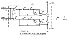
- FIG 4 is a schematic circuit diagram of an alternative output buffer 10b of the present invention.
- the first pull-up transistor N2 and the second pull-up transistor P2 of Figure 2 have been replaced with respective bipolar transitors Q1 and Q2.
- the first pull-down transistor P3 and the second pull-down transistor N3 have been replaced with respective bipolar transistors Q3 and Q4. Except for these differences, the operation of the output buffer 10b functions identically to the output buffer 10a described previously and thus will not be repeated.
- the present invention provides an improved output buffer for driving widely varying capacitive and inductive loads without significant output ringing.
- the output buffer of the present invention includes a pull-up circuit formed of a first pull-up transistor and a second pull-up transistor, and a pull-down circuit formed of a first pull-down transistor and a second pull-down transistor.
Abstract
Description
- This invention relates generally to integrated circuits and more particularly, it relates to an output buffer such as a full-level, fast CMOS output buffer for driving widely varying capacitive and inductive loads without significant output ringing.
- As is well known, digital logic circuits are widely used in the electronics field. One such use is for the interfacing between the logic of one integrated circuit device and another integrated circuit device. An output buffer is an important component for this interface function. The output buffer provides, when enabled, an output signal which is a function of a data input signal received from other logic circuitry of the integrated circuit.
- Output buffer circuits typically use a pull-up field-effect transistor (FET) and a pull-down field-effect transistor connected to an output node. Depending upon the state of data input signal and an enable signal, either the pull-up or pull-down field-effect transistor is quickly turned on and the other one of them is turned off.
- Such prior art output buffer circuits generally have the output node connected to an external pin of an integrated circuit for driving other circuitry on other integrated circuits which may have widely varying capacitive and inductive loading effects. When the output node is making a high-to-low or low-to-high transition, oscillation or inductive ringing appears on the output node of the buffer circuit as a function of the energy remaining in the parasitic interconnect inductances following the output transition and the impedance of the output driver in a circuit that includes the output loads, buffer drivers, and the ground loop.
- United States Patent Specification US-A-4,638,187 discloses a CMOS output buffer having field effect transistor pull-up and pull-down circuits which distribute switching current spikes over time. The pull-up circuit includes an P-channel FET and an N-channel FET connected in parallel between an output terminal and supply terminal VDD, with an inverter connected between the gates of the N-channel and P-channel FETs to provide the proper phase for the P-channel FETs as well as delaying turn-on of the P-channel FET with respect to the turn on the N-channel FET, and the N-channel FET shuts off when the output voltage reaches a certain potential. The pull down circuit includes a pair of N-channel FETs connected in parallel between the output terminal and ground, and a delay resistance connected between their gates so that turn-on of one of the N-channel FETs is delayed with respect to the other.
- It is desirable to provide an output buffer for driving widely varying capacitive and inductive loads which has a significant reduction in inductive ringing at an output node. The output buffer circuit to be described includes a pull-up circuit formed of a first pull-up transistor and a second pull-up transistor and a pull-down circuit formed of a first pull-down transistor and a second pull-down transistor. The reduction in the inductive ringing at the output node is achieved by increasing the driving transistors' equivalent impedance at the output node towards the end of either a low-to-high or high-to-low transition.
- Accordingly the present invention provides an output buffer for driving a load the capacitance and inductance of which may vary widely, with a reduction of inductive ringing at an output node thereof, comprising:
a pull-up circuit responsive to a first control signal, including a first pull-up transistor comprising a first N-channel transistor having its drain connected to a first supply voltage node and its source connected to said output node, and a second pull-up transistor comprising a first P-channel transistor having its source connected to said first supply potential, and its drain connected to said output node, and first and second inverters connected in series between a first control signal input to the buffer and the gate of said first N-channel transistor to control conduction thereof;
a pull-down circuit responsive to a second control signal, including a first pull-down transistor comprising a second P-channel transistor having its source connected to said output node and its drain connected to a second supply potential, and a second pull-down transistor comprising a second N-channel transistor having its drain connected to said output node and its source connected to said second supply potential, and third and fourth inverters connected in series between a second control signal input to the buffer and the gate of said second P-channel transistor to control conduction thereof;
said pull-up circuit further including a first NAND gate a first input of which is connected to said first control signal input to the buffer, a second input of which is connected to the output of said second inverter, and the output of which is connected to the gate of said first P-channel transistor; and
said pull-down circuit further including a first NOR gate a first input of which is connected to said second control signal input to the buffer, a second input of which is connected to the output of said fourth inverter, and the output of which is connected to the gate of said second N-channel transistor;
whereby the output impedance of the buffer is increased towards the end of an output transition of the buffer and energy stored in any parasitic inductance is decreased by said pull-up and pull-down transistors so as to reduce the inductive ringing while accelerating the completion of an output transition. - According to a further aspect of the invention there is provided an output buffer for driving a load the capacitance and inductance of which may vary widely, with a reduction of inductive ringing at an output node thereof, comprising:
a pull-up circuit responsive to a first control signal, including a first pull-up transistor comprising a first NPN transistor having its collector connected to a first supply voltage node and its emitter connected to said output node, and a second pull-up transistor comprising a first PNP transistor having its emitter connected to said first supply potential, and its collector connected to said output node, and first and second inverters connected in series between a first control signal input to the buffer and the base of said first NPN transistor to control conduction thereof;
a pull-down circuit responsive to a second control signal, including a first pull-down transistor comprising a second PNP transistor having its emitter connected to said output node and its collector connected to a second supply potential, and a second pull-down transistor comprising a second NPN transistor having its collector connected to said output node and its emitter connected to said second supply potential, and third and fourth inverters connected in series between a second control signal input to the buffer and the base of said second PNP transistor to control conduction thereof;
said pull-up circuit further including a first NAND gate a first input of which is connected to said first control signal input to the buffer, a second input of which is connected to the output of said second inverter, and the output of which is connected to the base of said first PNP transistor; and in that;
said pull-down circuit further including a first NOR gate a first input of which is connected to said second control signal input to the buffer, a second input of which is connected to the output of said fourth inverter, and the output of which is connected to the base of said second NPN transistor;
whereby the output impedance of the buffer is increased towards the end of an output transition of the buffer and energy stored in any parasitic inductance is decreased by said pull-up and pull-down transistors so as to reduce the inductive ringing while accelerating the completion of an output transition. - These and other advantages of the present invention will become more fully apparent from the following detailed description when read in conjunction with the accompanying drawings with like reference numerals indicating corresponding parts throughout, wherein:
- Figure 1 is a schematic circuit diagram of a prior art output buffer utilizing a P-channel pull-up FET and an N-channel pull-down FET;
- Figure 2 is a schematic circuit diagram of an output buffer constructed in accordance with the principles of the present invention;
- Figure 3 illustrates the voltages at the respective output nodes for both the prior art buffer circuit and the buffer circuit of the present invention; and
- Figure 4 is a schematic circuit diagram of an alternative output buffer constructed in accordance with the principles of the present invention using bipolar transistors.
- Referring now in detail to the drawings, there is shown in Figure 1 a schematic circuit diagram of a prior art
output buffer circuit 10 formed of a P-channel pull-up field-effect transistor (FET) P1 and an N-channel pull-down FET N1. Thebuffer circuit 10 provides an output signal at an output node A in response to a data input signalINPUT received at a data input node D and an enable signal ENABLE received at enable input node E. Thebuffer circuit 10 includes aNOR logic gate 12, aNAND logic gate 14, andinverters - The output node A of the
buffer circuit 10 is used to drive a varying capacitive and inductive load represented by impedance CAP. Further, the output node A is typically connected to aninternal node 22 via alead connection 24 having parasitic inductance L. - The NOR
logic gate 12 receives the data input signalINPUT online 26 on its one input and the enable signal ENABLE online 28 via theinverter 16 on its other input. The output of theNOR logic gate 12 online 30 is supplied to the gate of the P-channel pull-up transistor P1 via theinverter 18. The transistor P1 has its source connected via a lead line having parasitic inductance L(VCC) to a supply potential VCC, which is typically +5.0 volts, and has its drain connected via thelead connection 24 with the parasitic inductance L to the output node A. - The
NAND logic gate 14 receives the same data input signalINPUT online 26 on its one input and the same enable signal ENABLE on theline 28 on its other input. The output of theNAND gate 14 online 34 is applied to the gate of the N-channel pull-down transistor N1 via theinverter 20. The transistor N1 has its source connected via a lead line having parasitic inductance L(VSS)to a ground potential and its drain also connected via thelead connection 24 to the output node A. - When the enable signal ENABLE is at a high (VCC) or logic "1" level and the data input signal
INPUT is at a low or logic "0" level (GND), the output of theNOR gate 12 will be at the high logic level and the output of theNAND gate 14 will be at the high logic level. Due to theinverter 18, this causes a logic "0" (GND) to be applied to the gate of the transistor P1. Due to theinverter 20, this causes a logic "0" (GND) to be applied to the gate of the transistor N1. As a result, the P-channel transistor P1 is turned on and the N-channel N1 is turned off. Thus, the output node A is pulled towards the supply potential VCC. - On the other hand, when the enable signal ENABLE is at the high (VCC) or logic "1" level and the data input signal
INPUT is at a high (VCC) or logic "1" level, the output of theNOR gate 12 will be at the low or logic "0" level and the output of theNAND gate 14 will be at the low logic level. Due to theinverter 18, this causes a logic "1" (VCC) to be applied to the gate of the transistor P1. Due to theinverter 20, this causes a logic "1" (VCC) to be applied to the gate of the transistor N1. As a result, the P-channel transistor P1 is turned off and the N-channel transistor N1 is turned on. Thus, the output node A is pulled down towards the ground potential. - When the enable signal ENABLE is at the low or logic "0" level (GND), the output of the
NOR gate 12 is at the low or logic "0" level and the output of theNAND gate 14 is at the high or logic "1" level. Consequently, both of the transistors P1 and N1 are caused to be turned off. This produces a high impedance tri-state mode at the output node A in which theoutput buffer circuit 10 is not enabled. - The magnitude of the voltage at the output node A in the
buffer circuit 10 is dependent upon the capacitive and inductive load or impedance CAP being driven and the parasitic inductances. Dependent upon the logic state of the data input signalINPUT when the enable signal ENABLE is activated, either the pull-up or pull-down FET is quickly turned on and the other one of them is turned off. Such rapid switching on of the pull-up or pull-down field-effect transistors causes sudden surges of current commonly known as current spikes. These current spikes will flow through the parasitic inductances in the lead connections so as to cause oscillations or inductive ringing at the output node A of thebuffer circuit 10. - In Figure 2 there is shown an output buffer circuit 10a of the present invention which represents an improvement over the
buffer circuit 10 of Figure 1. The buffer circuit 10a provides the capability of driving quickly output loads that vary widely in capacitance and inductance to full-levels but yet reduces significantly the inductive ringing in the output signal due to the pull-up and pull-down output drivers switching states. The output buffer circuit 10a provides an output signal at an output node B in response to a data input signalINPUT received at data input node F and an enable signal ENABLE received at enable input node G. - The output buffer circuit 10a includes a NOR
logic gate 36, aNAND logic gate 40, aninverter 44, a pull-upcircuit 37, and a pull-down circuit 39. The pull-upcircuit 37 includesinverters NAND logic gate 42; and a second pull-up P-channel transistor P2. The pull-down circuit 39 includesinverters logic gate 38; and a second pull-down N-channel transistor N3. Similarly, the output node B is connected to an internal node C via alead connection 56 having parasitic inductance L. A widely varying capacitive and inductive load represented by impedance CAP is connected between the output node B and a ground potential. - The NOR
logic gate 36 receives the data input signalINPUT online 58 on its one input and the enable signal ENABLE online 60 via theinverter 44 on its other input. The output of the NORgate 36 provides a first control signal and is inverted twice by theinverters inverter 48 is connected to the gate of the first pull-up transistor N2 and to one input of theNAND gate 42. The output of the NORlogic gate 36 is also connected to the other input of theNAND gate 42. The first pull-up transistor N2 has its drain connected via a lead line having parasitic inductance L(VCC) to a supply potential VCC and its source connected via a lead line having parasitic inductance L to the output node B. The output of theNAND gate 42 is connected to the gate of the second pull-up transistor P2. The second pull-up transistor P2 has its source connected also via the line with the parasitic inductance L(VCC) to the supply potential VCC and its drain connected via theline 56 to the output node B. - The
NAND logic gate 40 receives the same data input signalINPUT online 58 on its one input and the same enable signal ENABLE online 60 on its other input. The output of theNAND logic gate 40 provides a second control signal and is inverted twice by theinverters inverter 52 is connected to the gate of the first pull-down transistor P3 and to one input of the NORgate 38. The output of theNAND gate 40 is also connected to the other input of the NORgate 38. The first pull-down transistor P3 has its source connected via theline 56 to the output node B and its drain connected via the line with the parasitic inductance L(VSS) to the ground potential. The output of the NORgate 38 is connected to the gate of the second pull-down transistor N3. The second pull-down transistor N3 has its drain connected also via theline 56 to the output node B and its source connected via the line with the parasitic inductance L(VSS) to the ground potential. - The operation of the buffer circuit 10a of Figure 2 will now be described. In particular, the pull-up action in Figure 2 will first be explained. The voltages at the nodes A, B and C are illustrated in Figure 3. When the output node B is to be pulled to the high or logic "1" level, the enable signal ENABLE must be at the high logic level and the data input signal
INPUT must be at the low logic level. Thus, the output of the NORgate 36 is at the high logic level. Due to theinverters inverter 48 will be at the high logic level. This causes the first pull-up transistor N2 to turn on and after a delay from theNAND gate 42, the second pull-up transistor P2 will also be turned on since the output of theNAND gate 42 will be at a low logic level. - The pull-up action is started initially by the turning on of the first pull-up transistor N2 followed quickly by the turning on of the second pull-up transistor P2. The transistors N2 and P2 supply current to drive the output node B from the low logic state to the high logic state. The voltage on node C leads the voltage on node B as current in parasitic interconnect inductance L builds up to a peak in the early part of the transition due to both transistors N2 and P2 having turned on with the maximum drain-to-source voltage. As the voltage on node C increases further, the current in inductance L decreases causing the voltage on node C to lag the voltage on the output node B. As the voltage on node C approaches one threshold drop below the supply potential VCC, the first pull-up transistor N2 turns off increasing the output impedance. This increased output impedance has two effects: (1) the drive current in the interconnect inductance L is reduced earlier in the transition and more quickly than in an equivalent prior art output buffer dissipating the energy stored in the interconnect inductance and causing the voltage across inductance L to increase temporarily; and (2) the low-to-high transition rate of node C is reduced with a subsequent damped response. The resulting response of output node B reflects the dampened response of node C with an offset voltage in the parasitic inductance L that accelerates the completion of the output transition.
- If the parasitic inductance L is sufficiently large, there is one further effect that reduces the energy stored in the parasitic interconnect inductance and thus reduces the output ringing. In the early stages of the transition the voltage on node C leads that on node B approaching a threshold below the supply voltage VCC causing the first pull-up transistor N2 to turn off. This reduces the drive current causing the voltage on the node C to quickly lag that on the output node B and fall once again turning on the transistor N2. Since the pull-up transistor N2 is off in part of the early stages of the output transition, the drive current level reaches in the interconnect inductance L is reduced relative to that reached by a comparable prior art output buffer. The remainder of the transition continues as previously described and is illustrated in Figure 3.
- The pull-down action in Figure 2 will be next explained. When the output node B is to be pulled to the low logic level, the enable signal ENABLE must be at a high logic level and the data input signal
INPUT must be at a high logic level. Thus, the output of theNAND logic gate 40 will be at a low logic level. Due to theinverter inverter 52 will be at a low logic level. This causes the first pull-down transistor P3 to be turned on and after a delay from the NORlogic gate 38, the second pull-down transistor N3 will also be turned on. - The pull-down action is started initially by the turning on of the first pull-down transistor P3 followed by the turning on of the second pull-down transistor N3. The transistors P3 and N3 supply current to drive the output node B from the high logic state to the low logic state. The voltage on node C leads the voltage on node B as current in inductance L builds up to a peak in the early part of the transition due to both transistors P3 and N3 having turned on with the maximum drain-to-source voltage. As the voltage on node C decreases further, the current in inductance L decreases causing the voltage on node C to lag the voltage on the output node B. As the voltage on node C approaches a threshold drop above ground potential VSS, the first pull-down transistor P3 turns off increasing the output impedance. This increased output impedance has two effects: (1) the drive current in the parasitic interconnect inductance L is reduced earlier in the transition and more quickly than in an equivalent conventional output buffer dissipating the energy stored in the interconnect inductance L and causing the voltage across inductance L to increase temporarily; and (2) the high-to-low transition rate of node C is reduced with a subsequent damped response. The resulting response of output node B reflects the dampened response of node c with an offset voltage in the parasitic inductance L that accelerates the completion of the output transition.
- If the parasitic inductance L is sufficiently large, there is one further effect that reduces the energy stored in the parasitic interconnect inductance and thus reduces the output ringing. In the early stages of the transition the voltage on node C leads that on node B approaching a threshold above the ground potential VSS causing the first pull-down transistor P3 to turn off. This reduces the drive current causing the voltage on the node C to quickly lag that on the output node B and rise once again turning on the transistor P3. Since the pull-down transistor P3 is off in part of the early stages of the output transition, the drive current level reached in the interconnect inductance L is reduced relative to that reached by a comparable prior art output buffer. The remainder of the transition continues as previously described and is illustrated in Figure 3.
- When the output node B is again required to be switched back to the high logic level (i.e., the output of the
NAND logic gate 40 goes to a high or logic "1"), the second input of the NORlogic gate 38 online 66 is used to bypass the delay which would otherwise be experienced due to theinverters logic gate 36 goes to a high or logic "1"), the second input of theNAND gate 42 online 68 is used to bypass the delay which would otherwise by experienced due to theinverters - In Figure 3, there are shown for comparison a computer simulation of the voltages at the output node A for the prior
art buffer circuit 10 and the nodes B and C for the buffer circuit 10a of the present invention. The waveform A of Figure 3 illustrates the voltage at the output node A of Figure 1 in response to when the data input signalINPUT makes a first high-to-low transition and a second low-to-high transition. The waveforms B and C of Figure 3 illustrate the corresponding voltages at the output node B and the node C of Figure 2 in response to when the data input signalINPUT makes a first high-to-low transition and a second low-to-high transition. By comparing the waveforms A and B, it can thus be seen that the overshooting of the supply potential of +5 volts in the buffer circuit of Figure 2 is about one volt less than the prior art buffer circuit in Figure 1. Yet, the initial rise times in making the low-to-high transition at the respective output nodes A and B are substantially the same. - Figure 4 is a schematic circuit diagram of an alternative output buffer 10b of the present invention. As can be seen, the first pull-up transistor N2 and the second pull-up transistor P2 of Figure 2 have been replaced with respective bipolar transitors Q1 and Q2. Further, the first pull-down transistor P3 and the second pull-down transistor N3 have been replaced with respective bipolar transistors Q3 and Q4. Except for these differences, the operation of the output buffer 10b functions identically to the output buffer 10a described previously and thus will not be repeated.
- From the foregoing detailed description, it can be seen that the present invention provides an improved output buffer for driving widely varying capacitive and inductive loads without significant output ringing. The output buffer of the present invention includes a pull-up circuit formed of a first pull-up transistor and a second pull-up transistor, and a pull-down circuit formed of a first pull-down transistor and a second pull-down transistor.
Claims (11)
- An output buffer (10a) for driving a load the capacitance and inductance of which may vary widely, with a reduction of inductive ringing at an output node (8) thereof, comprising:
a pull-up circuit (37) responsive to a first control signal, including a first pull-up transistor comprising a first N-channel transistor (N2) having its drain connected to a first supply voltage node (VCC) and its source connected to said output node (8), and a second pull-up transistor comprising a first P-channel transistor (P2) having its source connected to said first supply potential (VCC), and its drain connected to said output node (8), and first (46) and second (48) inverters connected in series between a first control signal input to the buffer and the gate of said first N-channel transistor (N2) to control conduction thereof;
a pull-down circuit (39) responsive to a second control signal, including a first pull-down transistor comprising a second P-channel transistor (P3) having its source connected to said output node (8) and its drain connected to a second supply potential (VSS), and a second pull-down transistor comprising a second N-channel transistor (N3) having its drain connected to said output node (8) and its source connected to said second supply potential (VSS), and third (50) and fourth (52) inverters connected in series between a second control signal input to the buffer and the gate of said second P-channel transistor (P3) to control conduction thereof;
said pull-up circuit (37) further including a first NAND gate (42) a first input of which is connected to said first control signal input to the buffer, a second input of which is connected to the output of said second inverter (48), and the output of which is connected to the gate of said first P-channel transistor (P2); and
said pull-down circuit (39) further including a first NOR gate (38) a first input of which is connected to said second control signal input to the buffer, a second input of which is connected to the output of said fourth inverter (52), and the output of which is connected to the gate of said second N-channel transistor (N3);
whereby the output impedance of the buffer is increased towards the end of an output transition of the buffer and energy stored in any parasitic inductance is decreased by said pull-up and pull-down transistors so as to reduce the inductive ringing while accelerating the completion of an output transition. - An output buffer (10a) for driving a load the capacitance and inductance of which may vary widely, with a reduction of inductive ringing at an output node (8) thereof, comprising:
a pull-up circuit (37) responsive to a first control signal, including a first pull-up transistor comprising a first NPN transistor (Q1) having its collector connected to a first supply voltage node (VCC) and its emitter connected to said output node (8), and a second pull-up transistor comprising a first PNP transistor (Q2) having its emitter connected to said first supply potential (VCC), and its collector connected to said output node (8), and first (46) and second (48) inverters connected in series between a first control signal input to the buffer and the base of said first NPN transistor (Q1) to control conduction thereof;
a pull-down circuit (39) responsive to a second control signal, including a first pull-down transistor comprising a second PNP transistor (Q3) having its emitter connected to said output node (8) and its collector connected to a second supply potential (VSS), and a second pull-down transistor comprising a second NPN transistor (Q4) having its collector connected to said output node (8) and its emitter connected to said second supply potential (VSS), and third (50) and fourth (52) inverters connected in series between a second control signal input to the buffer and the base of said second PNP transistor (Q3) to control conduction thereof;
said pull-up circuit (37) further including a first NAND gate (42) a first input of which is connected to said first control signal input to the buffer, a second input of which is connected to the output of said second inverter (48), and the output of which is connected to the base of said first PNP transistor (Q2); and in that;
said pull-down circuit (39) further including a first NOR gate (38) a first input of which is connected to said second control signal input to the buffer, a second input of which is connected to the output of said fourth inverter (52), and the output of which is connected to the base of said second NPN transistor (Q4);
whereby the output impedance of the buffer is increased towards the end of an output transition of the buffer and energy stored in any parasitic inductance is decreased by said pull-up and pull-down transistors so as to reduce the inductive ringing while accelerating the completion of an output transition. - An output buffer as claimed in Claim 1 or 2, characterised in that said second pull-up transistor (P2,Q2) and said second pull-down transistor (N3,Q4) are delayed in their turn-on times relative to the said first pull-up transistor (N2,Q1) and said first pull-down transistor (P3,Q3) respectively.
- An output buffer as claimed in any preceding claim, characterised by first logic means (36) arranged to generate said first control signal in response to a data input signal (INPUT) to the buffer changing from a high level to a low level.
- An output buffer as claimed in Claim 4, characterised in that said first logic means (36) comprises a second NOR gate.
- An output buffer as claimed in any preceding claim, characterised by second logic means (40) arranged to generate said second control signal in response to a data input signal (INPUT) to the buffer changing from a low level to a high level.
- An output buffer as claimed in Claim 6, characterised in that said second logic means (40) comprises a second NAND gate.
- An output buffer as claimed in any preceding claim, characterised in that when in operation, said first pull-up transistor (N2,Q1) is initially turned on followed quickly by the turning on of said second pull-up transistor (P2,Q2) for causing a change from low to high level at the output node, and wherein said first pull-up transistor (N2,Q1) turns off after the change from low to high level at the output node so as to increase the output impedance.
- An output buffer as claimed in Claim 8, characterised in that when in operation, said first pull-down transistor (P3,Q3) is initially turned on followed quickly by the turning on of said second pull-down transistor (N3,Q4) for causing a change from high to low level at the output node, and wherein said first pull-down transistor (P3,Q3) turns off after the change from high to low level at the output node so as to increase the output impedance.
- An output buffer as claimed in any preceding claim, characterised in that when in operation, said first NOR gate (38) is caused by said second control signal to quickly turn off the second pull-down transistor (N3,Q4) when the output node changes from low to high level.
- An output buffer as claimed in any preceding claim, characterised in that when in operation, said first NAND gate (42) is caused by said first control signal to quickly turn off the second pull-up transistor (P2,Q2) when the output node changes from high to low level.
Priority Applications (1)
| Application Number | Priority Date | Filing Date | Title |
|---|---|---|---|
| AT89300583T ATE103434T1 (en) | 1988-02-11 | 1989-01-23 | OUTPUT BUFFER. |
Applications Claiming Priority (2)
| Application Number | Priority Date | Filing Date | Title |
|---|---|---|---|
| US07/154,723 US4825101A (en) | 1988-02-11 | 1988-02-11 | Full-level, fast CMOS output buffer |
| US154723 | 1988-02-11 |
Publications (3)
| Publication Number | Publication Date |
|---|---|
| EP0329285A2 EP0329285A2 (en) | 1989-08-23 |
| EP0329285A3 EP0329285A3 (en) | 1990-09-19 |
| EP0329285B1 true EP0329285B1 (en) | 1994-03-23 |
Family
ID=22552499
Family Applications (1)
| Application Number | Title | Priority Date | Filing Date |
|---|---|---|---|
| EP89300583A Expired - Lifetime EP0329285B1 (en) | 1988-02-11 | 1989-01-23 | Output buffer |
Country Status (5)
| Country | Link |
|---|---|
| US (1) | US4825101A (en) |
| EP (1) | EP0329285B1 (en) |
| JP (1) | JP3044351B2 (en) |
| AT (1) | ATE103434T1 (en) |
| DE (1) | DE68914012T2 (en) |
Families Citing this family (40)
| Publication number | Priority date | Publication date | Assignee | Title |
|---|---|---|---|---|
| JPH01161916A (en) * | 1987-12-18 | 1989-06-26 | Toshiba Corp | Semiconductor integrated circuit |
| US5045722A (en) * | 1989-11-14 | 1991-09-03 | Advanced Micro Devices, Inc. | Output buffer preconditioning circuit |
| US5010261A (en) * | 1989-12-08 | 1991-04-23 | General Electric Company | Lossless gate driver circuit for a high frequency converter |
| JP2639207B2 (en) * | 1989-12-08 | 1997-08-06 | 日本電気株式会社 | Output circuit |
| US5121013A (en) * | 1990-02-12 | 1992-06-09 | Advanced Micro Devices, Inc. | Noise reducing output buffer circuit with feedback path |
| US5081374A (en) * | 1990-02-22 | 1992-01-14 | National Semiconductor Corporation | Output buffer circuit with signal feed forward for reducing switching induced noise |
| US5039874A (en) * | 1990-03-15 | 1991-08-13 | Hewlett-Packard Company | Method and apparatus for driving an integrated-circuit output pad |
| JP3426608B2 (en) * | 1990-04-04 | 2003-07-14 | ユニシス コーポレイシヨン | Clock deskew circuit |
| JPH0722758B2 (en) * | 1990-04-24 | 1995-03-15 | 群馬大学長 | Wastewater treatment method to remove organic matter and nitrogen at the same time |
| US5001369A (en) * | 1990-07-02 | 1991-03-19 | Micron Technology, Inc. | Low noise output buffer circuit |
| US5019728A (en) * | 1990-09-10 | 1991-05-28 | Ncr Corporation | High speed CMOS backpanel transceiver |
| US5122690A (en) * | 1990-10-16 | 1992-06-16 | General Electric Company | Interface circuits including driver circuits with switching noise reduction |
| JPH04153761A (en) * | 1990-10-17 | 1992-05-27 | Nec Corp | Output buffer |
| US5059823A (en) * | 1990-10-22 | 1991-10-22 | Advanced Micro Devices, Inc. | Supply bounce controlled output buffer circuit |
| JPH04192716A (en) * | 1990-11-26 | 1992-07-10 | Mitsubishi Electric Corp | Mos transistor output circuit |
| US5194765A (en) * | 1991-06-28 | 1993-03-16 | At&T Bell Laboratories | Digitally controlled element sizing |
| US5214322A (en) * | 1991-07-15 | 1993-05-25 | Unitrode Corporation | High voltage cmos power driver |
| KR930008656B1 (en) * | 1991-07-19 | 1993-09-11 | 삼성전자 주식회사 | Data output buffer for noise protected |
| US5319260A (en) * | 1991-07-23 | 1994-06-07 | Standard Microsystems Corporation | Apparatus and method to prevent the disturbance of a quiescent output buffer caused by ground bounce or by power bounce induced by neighboring active output buffers |
| US5233238A (en) * | 1991-12-20 | 1993-08-03 | Vlsi Technology, Inc. | High power buffer with increased current stability |
| US5254890A (en) * | 1992-01-16 | 1993-10-19 | Acer Incorporated | Ground bouncing reducing circuit and method |
| EP0552941B1 (en) * | 1992-01-21 | 1998-07-08 | STMicroelectronics, Inc. | Signal line pulse enhancing circuit for integrated circuits |
| JPH05243940A (en) * | 1992-02-27 | 1993-09-21 | Mitsubishi Electric Corp | Output buffer device |
| US5576640A (en) * | 1992-09-25 | 1996-11-19 | At&T Global Information Solutions Company | CMOS driver for fast single-ended bus |
| US5426376A (en) * | 1993-04-23 | 1995-06-20 | Vlsi Technology, Inc. | Noise isolated I/O buffer that uses two separate power supplies |
| US5488322A (en) * | 1994-08-29 | 1996-01-30 | Kaplinsky; Cecil H. | Digital interface circuit with dual switching points for increased speed |
| EP0717501A1 (en) * | 1994-12-15 | 1996-06-19 | Advanced Micro Devices, Inc. | Programmable drive buffer |
| US5550486A (en) * | 1995-03-01 | 1996-08-27 | Texas Instruments Incorporated | Circuit and method for providing a known logic state at insufficient supply voltage |
| EP0735676B1 (en) * | 1995-03-29 | 2001-05-23 | Agilent Technologies, Inc. | Predriver circuit for low-noise switching of high currents in a load |
| TW299527B (en) * | 1996-02-28 | 1997-03-01 | Hewlett Packard Co | Reduced switching current buffer amplifier |
| US5708386A (en) * | 1996-03-28 | 1998-01-13 | Industrial Technology Research Institute | CMOS output buffer with reduced L-DI/DT noise |
| US6008684A (en) * | 1996-10-23 | 1999-12-28 | Industrial Technology Research Institute | CMOS output buffer with CMOS-controlled lateral SCR devices |
| US5781050A (en) * | 1996-11-15 | 1998-07-14 | Lsi Logic Corporation | Open drain output driver having digital slew rate control |
| US5920210A (en) * | 1996-11-21 | 1999-07-06 | Kaplinsky; Cecil H. | Inverter-controlled digital interface circuit with dual switching points for increased speed |
| KR100242987B1 (en) * | 1996-11-27 | 2000-02-01 | 김영환 | 5v tolerant input/output circuit |
| US6097238A (en) * | 1997-01-10 | 2000-08-01 | Xilinx, Inc. | Circuit with ramp-up control and overcoming a threshold voltage loss in an NMOS transistor |
| US6091259A (en) * | 1997-08-29 | 2000-07-18 | Sun Microsystems, Inc. | Apparatus for accelerating digital signal transitions using a transition acceleration circuit and a transition termination circuit |
| US6281706B1 (en) * | 1998-03-30 | 2001-08-28 | National Semiconductor Corp. | Programmable high speed quiet I/O cell |
| US6236245B1 (en) * | 1999-06-11 | 2001-05-22 | Triscend Corporation | Output pre-driver for reducing totem pole current |
| US20120070444A1 (en) | 2007-01-19 | 2012-03-22 | Probiodrug Ag | IN VIVO SCREENING MODELS FOR TREATMENT OF isoQC-RELATED DISORDERS |
Citations (1)
| Publication number | Priority date | Publication date | Assignee | Title |
|---|---|---|---|---|
| US4638187A (en) * | 1985-10-01 | 1987-01-20 | Vtc Incorporated | CMOS output buffer providing high drive current with minimum output signal distortion |
Family Cites Families (12)
| Publication number | Priority date | Publication date | Assignee | Title |
|---|---|---|---|---|
| US4540904A (en) * | 1983-05-03 | 1985-09-10 | The United States Of America As Represented By The Secretary Of The Air Force | Tri-state type driver circuit |
| JPS60125015A (en) * | 1983-12-12 | 1985-07-04 | Hitachi Ltd | Inverter circuit |
| US4567378A (en) * | 1984-06-13 | 1986-01-28 | International Business Machines Corporation | Driver circuit for controlling signal rise and fall in field effect transistor processors |
| US4684824A (en) * | 1985-04-02 | 1987-08-04 | Eastman Kodak Company | Capacitive load driver circuit |
| KR920006438B1 (en) * | 1985-04-22 | 1992-08-06 | 엘 에스 아이 로직 코포레이션 | High-speed cmos buffer with controlled slew rate |
| GB2184622B (en) * | 1985-12-23 | 1989-10-18 | Philips Nv | Outputbuffer and control circuit providing limited current rate at the output |
| JPS62220026A (en) * | 1986-03-20 | 1987-09-28 | Toshiba Corp | Output buffer circuit |
| EP0253914A1 (en) * | 1986-07-23 | 1988-01-27 | Deutsche ITT Industries GmbH | Insulated-gate field-effect transistor push-pull driver stage with compensation for fluctuations of working parameters and variations in manufacturing process |
| US4749882A (en) * | 1986-07-25 | 1988-06-07 | Digital Equipment Corporation | Apparatus and method for applying rapid transient signals to components on a printed circuit board |
| JPS6382122A (en) * | 1986-09-26 | 1988-04-12 | Toshiba Corp | Logic circuit |
| US4731553A (en) * | 1986-09-30 | 1988-03-15 | Texas Instruments Incorporated | CMOS output buffer having improved noise characteristics |
| US4785201A (en) * | 1986-12-29 | 1988-11-15 | Integrated Device Technology, Inc. | High speed/high drive CMOS output buffer with inductive bounce suppression |
-
1988
- 1988-02-11 US US07/154,723 patent/US4825101A/en not_active Expired - Lifetime
-
1989
- 1989-01-23 DE DE68914012T patent/DE68914012T2/en not_active Expired - Fee Related
- 1989-01-23 AT AT89300583T patent/ATE103434T1/en not_active IP Right Cessation
- 1989-01-23 EP EP89300583A patent/EP0329285B1/en not_active Expired - Lifetime
- 1989-02-09 JP JP1030932A patent/JP3044351B2/en not_active Expired - Lifetime
Patent Citations (2)
| Publication number | Priority date | Publication date | Assignee | Title |
|---|---|---|---|---|
| US4638187A (en) * | 1985-10-01 | 1987-01-20 | Vtc Incorporated | CMOS output buffer providing high drive current with minimum output signal distortion |
| US4638187B1 (en) * | 1985-10-01 | 1993-03-02 | Cypress Semiconductor Minnesot |
Also Published As
| Publication number | Publication date |
|---|---|
| JPH027716A (en) | 1990-01-11 |
| DE68914012D1 (en) | 1994-04-28 |
| ATE103434T1 (en) | 1994-04-15 |
| DE68914012T2 (en) | 1994-09-08 |
| EP0329285A2 (en) | 1989-08-23 |
| US4825101A (en) | 1989-04-25 |
| JP3044351B2 (en) | 2000-05-22 |
| EP0329285A3 (en) | 1990-09-19 |
Similar Documents
| Publication | Publication Date | Title |
|---|---|---|
| EP0329285B1 (en) | Output buffer | |
| US5124579A (en) | Cmos output buffer circuit with improved ground bounce | |
| EP0303341B1 (en) | Output buffer circuits | |
| US5332932A (en) | Output driver circuit having reduced VSS/VDD voltage fluctuations | |
| US5568062A (en) | Low noise tri-state output buffer | |
| US4902914A (en) | Logic circuit used in standard IC or CMOS logic level | |
| KR20010049227A (en) | Level adjustment circuit and data output circuit thereof | |
| US5801550A (en) | Output circuit device preventing overshoot and undershoot | |
| US5097148A (en) | Integrated circuit buffer with improved drive capability | |
| US6121789A (en) | Output buffer with control circuitry | |
| US5438278A (en) | High speed CMOS output buffer circuit minimizes propagation delay and crowbar current | |
| US5233238A (en) | High power buffer with increased current stability | |
| US5121000A (en) | Edge-rate feedback CMOS output buffer circuits | |
| US11711079B2 (en) | Integrated bus interface fall and rise time accelerator method | |
| US4918332A (en) | TTL output driver gate configuration | |
| WO1996019871A1 (en) | Negative feedback to reduce voltage oscillation in cmos output buffers | |
| US6281708B1 (en) | Tri-state bus amplifier-accelerator | |
| US5864245A (en) | Output circuit with overvoltage protection | |
| JP2573431B2 (en) | Output buffer circuit | |
| US5160860A (en) | Input transition responsive CMOS self-boost circuit | |
| JPH0752829B2 (en) | Output circuit | |
| EP1009097A1 (en) | Variable driver for reducing overshoot, undershoot, and noise in an output buffer | |
| JPH0583122A (en) | Cmos logic circuit | |
| JPH02100516A (en) | Semiconductor output circuit | |
| JPH0697801A (en) | Input circuit |
Legal Events
| Date | Code | Title | Description |
|---|---|---|---|
| PUAI | Public reference made under article 153(3) epc to a published international application that has entered the european phase |
Free format text: ORIGINAL CODE: 0009012 |
|
| AK | Designated contracting states |
Kind code of ref document: A2 Designated state(s): AT BE CH DE ES FR GB GR IT LI LU NL SE |
|
| PUAL | Search report despatched |
Free format text: ORIGINAL CODE: 0009013 |
|
| AK | Designated contracting states |
Kind code of ref document: A3 Designated state(s): AT BE CH DE ES FR GB GR IT LI LU NL SE |
|
| 17P | Request for examination filed |
Effective date: 19901217 |
|
| 17Q | First examination report despatched |
Effective date: 19920605 |
|
| GRAA | (expected) grant |
Free format text: ORIGINAL CODE: 0009210 |
|
| AK | Designated contracting states |
Kind code of ref document: B1 Designated state(s): AT BE CH DE ES FR GB GR IT LI LU NL SE |
|
| PG25 | Lapsed in a contracting state [announced via postgrant information from national office to epo] |
Ref country code: NL Effective date: 19940323 Ref country code: LI Effective date: 19940323 Ref country code: GR Free format text: LAPSE BECAUSE OF FAILURE TO SUBMIT A TRANSLATION OF THE DESCRIPTION OR TO PAY THE FEE WITHIN THE PRESCRIBED TIME-LIMIT Effective date: 19940323 Ref country code: ES Free format text: THE PATENT HAS BEEN ANNULLED BY A DECISION OF A NATIONAL AUTHORITY Effective date: 19940323 Ref country code: CH Effective date: 19940323 Ref country code: BE Effective date: 19940323 Ref country code: AT Effective date: 19940323 |
|
| REF | Corresponds to: |
Ref document number: 103434 Country of ref document: AT Date of ref document: 19940415 Kind code of ref document: T |
|
| REF | Corresponds to: |
Ref document number: 68914012 Country of ref document: DE Date of ref document: 19940428 |
|
| ITF | It: translation for a ep patent filed |
Owner name: ING. C. GREGORJ S.P.A. |
|
| REG | Reference to a national code |
Ref country code: CH Ref legal event code: PL |
|
| ET | Fr: translation filed | ||
| NLV1 | Nl: lapsed or annulled due to failure to fulfill the requirements of art. 29p and 29m of the patents act | ||
| PLBE | No opposition filed within time limit |
Free format text: ORIGINAL CODE: 0009261 |
|
| STAA | Information on the status of an ep patent application or granted ep patent |
Free format text: STATUS: NO OPPOSITION FILED WITHIN TIME LIMIT |
|
| EAL | Se: european patent in force in sweden |
Ref document number: 89300583.5 |
|
| PG25 | Lapsed in a contracting state [announced via postgrant information from national office to epo] |
Ref country code: LU Free format text: LAPSE BECAUSE OF NON-PAYMENT OF DUE FEES Effective date: 19950131 |
|
| 26N | No opposition filed | ||
| PGFP | Annual fee paid to national office [announced via postgrant information from national office to epo] |
Ref country code: GB Payment date: 19980108 Year of fee payment: 10 |
|
| PGFP | Annual fee paid to national office [announced via postgrant information from national office to epo] |
Ref country code: SE Payment date: 19980205 Year of fee payment: 10 |
|
| PGFP | Annual fee paid to national office [announced via postgrant information from national office to epo] |
Ref country code: DE Payment date: 19980227 Year of fee payment: 10 |
|
| PG25 | Lapsed in a contracting state [announced via postgrant information from national office to epo] |
Ref country code: GB Free format text: LAPSE BECAUSE OF NON-PAYMENT OF DUE FEES Effective date: 19990123 |
|
| PG25 | Lapsed in a contracting state [announced via postgrant information from national office to epo] |
Ref country code: SE Free format text: LAPSE BECAUSE OF NON-PAYMENT OF DUE FEES Effective date: 19990124 |
|
| GBPC | Gb: european patent ceased through non-payment of renewal fee |
Effective date: 19990123 |
|
| PG25 | Lapsed in a contracting state [announced via postgrant information from national office to epo] |
Ref country code: DE Free format text: LAPSE BECAUSE OF NON-PAYMENT OF DUE FEES Effective date: 19991103 |
|
| PGFP | Annual fee paid to national office [announced via postgrant information from national office to epo] |
Ref country code: FR Payment date: 20020104 Year of fee payment: 14 |
|
| PG25 | Lapsed in a contracting state [announced via postgrant information from national office to epo] |
Ref country code: FR Free format text: LAPSE BECAUSE OF NON-PAYMENT OF DUE FEES Effective date: 20030930 |
|
| REG | Reference to a national code |
Ref country code: FR Ref legal event code: ST |
|
| PG25 | Lapsed in a contracting state [announced via postgrant information from national office to epo] |
Ref country code: IT Free format text: LAPSE BECAUSE OF NON-PAYMENT OF DUE FEES;WARNING: LAPSES OF ITALIAN PATENTS WITH EFFECTIVE DATE BEFORE 2007 MAY HAVE OCCURRED AT ANY TIME BEFORE 2007. THE CORRECT EFFECTIVE DATE MAY BE DIFFERENT FROM THE ONE RECORDED. Effective date: 20050123 |