EP0330475A2 - Configuration control system - Google Patents
Configuration control system Download PDFInfo
- Publication number
- EP0330475A2 EP0330475A2 EP89301785A EP89301785A EP0330475A2 EP 0330475 A2 EP0330475 A2 EP 0330475A2 EP 89301785 A EP89301785 A EP 89301785A EP 89301785 A EP89301785 A EP 89301785A EP 0330475 A2 EP0330475 A2 EP 0330475A2
- Authority
- EP
- European Patent Office
- Prior art keywords
- configuration control
- configuration
- clea
- storage unit
- gcfr
- Prior art date
- Legal status (The legal status is an assumption and is not a legal conclusion. Google has not performed a legal analysis and makes no representation as to the accuracy of the status listed.)
- Granted
Links
- 238000012545 processing Methods 0.000 claims abstract description 48
- 241000725101 Clea Species 0.000 description 22
- 238000010586 diagram Methods 0.000 description 9
- 101100332284 Saccharomyces cerevisiae (strain ATCC 204508 / S288c) DSS1 gene Proteins 0.000 description 3
- 230000005540 biological transmission Effects 0.000 description 3
- 101100191136 Arabidopsis thaliana PCMP-A2 gene Proteins 0.000 description 2
- 101100422768 Saccharomyces cerevisiae (strain ATCC 204508 / S288c) SUL2 gene Proteins 0.000 description 2
- 101100048260 Saccharomyces cerevisiae (strain ATCC 204508 / S288c) UBX2 gene Proteins 0.000 description 2
- 230000006870 function Effects 0.000 description 2
- 238000000034 method Methods 0.000 description 2
- 230000004044 response Effects 0.000 description 2
- 238000004891 communication Methods 0.000 description 1
- 238000007796 conventional method Methods 0.000 description 1
Images


Classifications
-
- G—PHYSICS
- G06—COMPUTING; CALCULATING OR COUNTING
- G06F—ELECTRIC DIGITAL DATA PROCESSING
- G06F11/00—Error detection; Error correction; Monitoring
- G06F11/07—Responding to the occurrence of a fault, e.g. fault tolerance
- G06F11/16—Error detection or correction of the data by redundancy in hardware
- G06F11/1666—Error detection or correction of the data by redundancy in hardware where the redundant component is memory or memory area
-
- G—PHYSICS
- G06—COMPUTING; CALCULATING OR COUNTING
- G06F—ELECTRIC DIGITAL DATA PROCESSING
- G06F15/00—Digital computers in general; Data processing equipment in general
- G06F15/16—Combinations of two or more digital computers each having at least an arithmetic unit, a program unit and a register, e.g. for a simultaneous processing of several programs
- G06F15/161—Computing infrastructure, e.g. computer clusters, blade chassis or hardware partitioning
-
- G—PHYSICS
- G06—COMPUTING; CALCULATING OR COUNTING
- G06F—ELECTRIC DIGITAL DATA PROCESSING
- G06F11/00—Error detection; Error correction; Monitoring
- G06F11/07—Responding to the occurrence of a fault, e.g. fault tolerance
- G06F11/16—Error detection or correction of the data by redundancy in hardware
- G06F11/20—Error detection or correction of the data by redundancy in hardware using active fault-masking, e.g. by switching out faulty elements or by switching in spare elements
Definitions
- the present invention relates to a configuration control system, more particularly, it relates to a control system for changing the system configuration of a data processing system.
- the configuration control system according to the present invention is advantageous for use in a large scale and complicated data processing system constituted by, for example, a plurality of clusters and at least one global storage unit, each cluster having a channel processing unit, at least one central processing unit, at least one main storage unit, a memory control unit and a service processor, and each of the global storage units supporting in common these plural clusters.
- the above type data processing system is divided into a current system and a stand-by system for achieving a high reliability and high speed processing in conjunction with each of the global storage units.
- each of the configuration control registers provided in the memory control unit and the global storage unit is usually performed by each of the configuration control registers provided in the memory control unit and the global storage unit. That is, each of the units constituting the cluster is connected to or disconnected from other units by turning ON/OFF ("1" or "0") a specific bit of the configuration control register.
- the system configuration is relatively small scale.
- a "non-stop system” (a"non-stop system” is one in which the operation of the system is not stopped when changing the system configuration) is not usually required by an end user. Accordingly, the configuration is only changed by the service processor using a general scan-in/out function usually provided in data processing systems. In this case, the central processing unit sends a command to change the configuration to the service processor and the service processor performs the above steps. Therefore, it is not necessary to add new configuration changing hardware to the data processing unit, and accordingly, it is possible to economically perform the configuration change.
- the configuration control register is operated by a clock signal different from the clock signal used to operate the cluster. Accordingly, the whole system must be temporarily stopped to ensure normal operation of the cluster.
- Recent data processing systems have become larger scale; for example, a typical large scale data processing system constitutes a plurality of clusters with global storage units for controlling each of the clusters as explained above.
- any one service processor can change the configuration of the whole system, and in this case, the whole system is stopped for a considerable length of time.
- a "non-stop system" enabling a change of the configuration without stopping the system is now required in large scale data processing systems to achieve a high speed control when changing a configuration.
- such a configuration control system also includes a second configuration control means for holding configuration control information of the at least one global storage unit and the plurality of clusters which is independently controlled from the first configuration control means; means for generating a specific order for writing/reading the configuration control information to the second configuration control means; and, means for setting a corresponding bit of the second configuration control means to a connection state when a bus between the at least one global storage unit and the plurality of clusters is set to the connection state by the first configuration control means; wherein the connection configuration between the at least one global storage unit and the plurality of clusters designated by the first configuration control means is automatically set to the second configuration control means, and the second configuration control means is controlled independently of the first configuration control means based on the specific order.
- This provides a configuration control system which enables a high speed control to be performed when changing the system configuration.
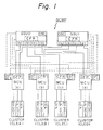
- FIG. 1 is a schematic block diagram of one example of a conventional data processing system having a large scale of a complicated system configuration.
- This data processing system GCMP is constituted by two global storage units GSU0 and GSU1 and clusters CLEA TO CLED.
- Each of the clusters CLEA to CLED comprises a service processor SVP, a memory control unit MCU, a channel processor CHP, central processing units CPU0 to CPU3, and main storage units MSU0 and MSU1, and each of the global storage units GSU0 and GSU1 supports in common the clusters CLEA to CLED.
- the configuration control register CFR is provided in each of memory control units MCU and each of the global storage units GSU.
- the reference letters (a) to (d) are interface sections including interface circuits, AND gates and the like.
- the system configuration can be changed in accordance with a requirement from, for example, the cluster CLEA, if a failure occurs in any other cluster.
- the change of the configuration is performed by changing the connection or disconnection between each of the units constituting the cluster. Such a connection or disconnection is performed by a specific bit from the configuration control register CFR or by a status indicating signal generated from each unit.
- the connection state of the cluster CLEA means that the all status indicating signals related to the cluster CLEA are "ON" and buses connected to the configuration control register CFR are activated (set to the online state).
- the information indicating the above states is stored in the main storage units MSU0 and MSU1 in each cluster CLEA to CLED, the configuration control information stored in the main storage units is updated by a specific program from the cluster, and the updated information is loaded from the main storage unit into the configuration control register CFR by the command from the service processor and held therein.
- FIG. 2 is a schematic block diagram for explaining the conventional control system for changing the system configuration. The operations are explained below.
- the central processing unit CPU in each cluster generates a specific order indicating a write operation to the service processor SVP, and sends a scan-out command to the service processor SVP.
- the service processor SVP receives this command, the service processor SVP generates the scan-out command CMD (20) and sends it to the configuration control register CFR (20-0 to 20-n).
- the contents of the configuration control register CFR i.e., the control information and the status indicating signal (PRDY-CLEA and URDY-CLEA) are scanned out through the selector SEL (21).
- the data scanned out from the configuration control register CFR is stored in the memory of the service processor SVP through the known SCI-interface.
- the service processor SVP When the service processor SVP receives the scan-out data, the service processor SVP generates configuration control information having a predetermined form based on the content of the configuration control register CFR and the status indicating signal.
- the configuration control information from the service processor SVP is stored in main storage unit MSU in the cluster designated by the store command from the service processor SVP.
- the service processor SVP sends an end information (END) signal to the central processing unit CPU in each cluster CLE.
- END end information
- the configuration control information stored in the main memory unit MSU can be updated by the specific program performed by the central processing unit CPU.
- the central processing unit CPU generates the specific order indicating a load operation and sends it to the service processor SVP, commanding the service processor SVP to perform the scan-in operation.
- the service processor SVP reads out the configuration control information from the main memory unit MSU and writes the configuration control information to the memory of the service processor SVP.
- the service processor SVP outputs the scan command, and the configuration control information is set to the configuration control register in each cluster with the status indicating signal possessed by each cluster, thus changing the content of the configuration control register.
- the service processor SVP sends the end information (END) signal to the central processing unit CPU in each cluster.
- each of AND gates 22 is provided for setting the interface 23 provided between the global storage unit GSU and the cluster CLE to the online state (ONLINE-CLEA to ONLINE-CLED).
- the corresponding bit of the configuration control register CFR is turned ON, and the states of the power-ON signal (PRDY-CLEA) and the state indicating signal (URDY-CLEA) of the cluster CLEA are then judged by the AND gate, with the result that, when all of the conditions mentioned above coincide, the interface 23 can be set to a valid state.
- Each of interface circuits A to D (23) is provided in the interface (a) to (d) in the global storage unit and connects the global control unit GSU and the corresponding memory control unit MCU.
- the control signal for example, a request signal (REQ) between the global storage unit GSU and the cluster CLEA to CLED is made valid by obtaining a conjunction of the output signal of the AND gate 22.
- configuration control register CFR since the configuration control register CFR must be rewritten prior to all other processings of the cluster, a general clock generated in the cluster is not used for rewriting the configuration control register to enable the rewriting of the configuration control register regardless of the states of the other units (for example, failure, clock stop state).
- a conventional configuration control is performed by the service processor. That is, the change of the content of the configuration control register is based on the scan-in/out operation of the scanning means and the read-write operation from and to the main memory unit at the command of the service processor SVP.
- the long processing time (about 5 to 6 seconds) is required in the conventional control system for changing the configuration.
- the whole system is temporarily stopped as explained above.
- This configuration control system is advantageously applied to a data processing system having a large scale and complicated system configuration as shown in Fig. 3.
- This data processing system GCMP is constituted by two global storage units GSU0 and GSU1 and clusters CLEA to CLED.
- Each of the clusters CLEA to CLED comprises a service processor SVP, a memory control unit MCU, a channel processor CHP, central processing units CPU0 to CPU3 and main storage units MSU0 and MSU1.
- the configuration control register CFR is provided in each of memory control units MCU and each of the global storage units GSU, as in the conventional system shown in Fig. 1.
- a new configuration control register GCFR according to the present invention is provided in each of the global storage units GSU0 and GSU1.
- the configuration control according to the present invention is performed between the global storage unit GSU and each of the clusters CLEA to CLED. According to the present invention, control of the change of the configuration can be performed at a high speed due to the relationship between the global storage unit GSU and each of the clusters CLEA to CLED in the data processing system shown in Fig. 3.
- a high reliability and “non-stop operation" of the system are required in a data processing system having a large scale and complicated configuration; for example, the system shown in Fig. 3.
- the "non-stop operation” means that the stop time required for changing the configuration of the system is very short (within 1 second), and thus is almost negligible. Accordingly, such a system is divided into two systems, i.e., a current system (GSU0 side), and a stand-by system (GSU1 side), to achieve the "non-stop operation".
- GSU0 side current system
- GSU1 side stand-by system
- the current system is disconnected and the processing performed in the current system is taken over by the stand-by system.
- the data processed by the current system is written to both global storage units, and if one global storage unit discovers a failure, that global storage unit is disconnected and the other global storage unit continues the processing. Accordingly, it is possible to obtain a data processing system having a high reliability and "non-stop operation" based on the above steps.
- the object of the present invention lies in the achievement of a high speed and "non-stop operation" of the data processing system.
- the basic steps therefor are explained hereinafter.
- a specific order is provided for writing/reading the configuration control information between the global storage unit and the cluster and the new configuration control register GCFR according to the present invention.
- the new configuration control register GCFR is provided in each of the global storage units GSU0 and GSU1, and AND gates are added to judge the online state between the global storage unit GSU and the cluster CLE. These AND gates are opened when obtaining the conjunction between the bit of the new configuration control register GCFR and the conventional configuration control register CFR.
- the configuration control information is written to the area of the main memory unit MSU designated by the write order by the same control as the data transmission control from the global storage unit GSU to the main memory unit MSU.
- the configuration control information held by the global storage unit is held on the read data bus from the global storage unit.
- the content of the area of the main memory unit MSU designated by the read order is set to the configuration control register GCFR by the same control as the data transmission control from the main storage unit MSU to the global storage unit GSU.
- the content of the data bus from the main storage unit to the global storage unit is the data of the change for rewriting the content of the configuration control register GCFR.
- the configuration control register GCFR can control the connection/disconnection between the cluster CLE and the global storage unit GSU, it is possible to control the change of the configuration (for example, connection/disconnection of the cluster when a failure occurs) without stopping the operation of the cluster CLE.
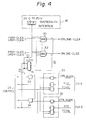
- Figure 4 is a schematic block diagram of a configuration control system according to the present invention.
- Fig. 4 denotes an interface unit having first configuration control registers CFR (20-0 to 20-n) each of which holds the connection information of each of the units in the cluster, and 31 denotes a second configuration control register GCFR holding the configuration control information between the global storage unit and the cluster. The specific order is provided for writing/reading the configuration control information to the second configuration control register GCFR.
- References 32 and 34 denote AND gates, and 33 denotes interface circuits.
- PRDY-CLEA and URDY-CLEA denote status indicating signals, the former denoting the power-ON signal of the cluster CLEA and the latter denoting the ready signal indicating the operation of each unit in the cluster CLEA.
- ONLINE-CLEA denotes the online state of the cluster CLEA.
- CTRL denotes the control signal, ADDR an address signal, STD a store data signal and FCHD a fetch data signal. Further, 1 and 2 denote write circuits, and 3 denotes a read circuit.
- Figure 5 is a detailed block diagram of the second configuration control register GCFR according to the present invention
- Fig. 6 is a signal timing chart of the second configuration control register shown in Fig. 5.
- DEC denotes a decoder and SEL1 and SEL2 selectors.
- Futher, CLEB-GCFR-SR denotes a set/reset signal from the cluster CLEB.
- the selector SEL1 selects one of the global storage units GSU0 and GSU1
- the selector SEL2 selects one of the configuration control registers CLEA to CLED based on the control signal CTRL.
- the same circuit as the above is provided for the clusters CLEB to CLED.
- the change of the system configuration is performed by the conventional configuration control register CFR shown in Fig. 2, through the service processor SVP, because it is not necessary to take the processing time into consideration for changing the configuration.
- the configuration control information is set to the first configuration control register CFR.
- each bit is constituted by a master-slave type flip-flop circuit C0 to C2 having a priority function for a reset operation (reset-priority type).
- the second configuration control register GCFR is also set to the reset state.
- the specific bit of the first configuration control register CFR is changed to the set state (i.e., changed from disconnection to connection)
- the corresponding bit of the second configuration control register GCFR (31) is simultaneously turned ON by a leading signal ⁇ of the AND gate A through the OR gate.
- the line connected between the global storage unit GSU and the cluster CLEA is activated and enters the online state (GCFR-CLEA-ONL).
- This method facilitates the initialization of the second configuration control register GCFR. Further, it is possible to easily include the disconnected clusters in the whole system.
- the change of the configuration for this case can be performed by only rewriting the content of the first configuration control register CFR.
- the change of the configuration for this case can be performed by directly rewriting the content of the second configuration control register GCFR using the specific order according to the present invention, so that it is possible to obtain the connection between the global storage unit GSU and the cluster CLE.
- This rewriting of the second configuration control register GCFR can be performed by the control signal CTRL/ADDR and the configuration control information STD, the control signal CTRL/ADDR being given by a specific order from all clusters entering the online state.
- Figure 6 is a signal timing chart for explaining the operation of the second configuration control register GCFR shown in Fig. 5.
- CLK-G0 denotes a clock signal generated from an oscillator OSC in the global storage unit GSU0
- CLEA-C0, C1, C2 denote a signal generated from each flip-flop circuit C0, C1, and C2.
- the signal ⁇ denotes the leading signal obtained from the AND gate A. That is, the signal ⁇ is obtained by the conjunction between the flip-flop C1 and the flip-flop C2.
- GCFR-CLEA-ONL denotes the online state between the global storage unit GSU and the cluster CLEA. This line is set or reset by the reset signal RST or the set signal SET.
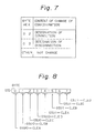
- Figure 7 shows the data of the change of the configuration.
- HEX denotes a hexadecimal number
- the designation of the connection is given by "BYTE 02" ("00000010")and the designation of the disconnection given by "BYTE 03" (00000011).
- designation of the non-change state is given by "OTHER" BYTE.
- FIG. 8 shows write data indicating the relationship between the global storage unit and the cluster.
- the write data STD is data on the write data bus used for normal data transmission from the main memory unit MSU to the global storage unit.
- the write data STD is transferred to the second configuration register GCFR through the interface 33 and written thereto as shown in Fig. 4 (write circuit 2).
- BYTE 0 denotes the relationship of the connection between the global storage unit GSU0 and the cluster CLEA.
- the write data STD of the "BYTE 0" is expressed by eight bits which are all "0”.
- BYTE 4 denotes the relationship of the connection between the global storage unit GSU1 and the cluster CLEA.
- the write data STD of the "BYTE 4" is expressed by eight bits as "00000100".
- the content of the second configuration control register GCFR is transferred to the data bus from the global storage unit GSU to the cluster CLE and written to the designated area of the main memory unit MSU of the cluster CLE as shown by 3 in Fig. 4.
Abstract
Description
- The present invention relates to a configuration control system, more particularly, it relates to a control system for changing the system configuration of a data processing system. The configuration control system according to the present invention is advantageous for use in a large scale and complicated data processing system constituted by, for example, a plurality of clusters and at least one global storage unit, each cluster having a channel processing unit, at least one central processing unit, at least one main storage unit, a memory control unit and a service processor, and each of the global storage units supporting in common these plural clusters. Usually, the above type data processing system is divided into a current system and a stand-by system for achieving a high reliability and high speed processing in conjunction with each of the global storage units.
- The management of the system configuration of the data processing system is usually performed by each of the configuration control registers provided in the memory control unit and the global storage unit. That is, each of the units constituting the cluster is connected to or disconnected from other units by turning ON/OFF ("1" or "0") a specific bit of the configuration control register.
- In this conventional data processing system, the system configuration is relatively small scale. Further, a "non-stop system" (a"non-stop system" is one in which the operation of the system is not stopped when changing the system configuration) is not usually required by an end user. Accordingly, the configuration is only changed by the service processor using a general scan-in/out function usually provided in data processing systems. In this case, the central processing unit sends a command to change the configuration to the service processor and the service processor performs the above steps. Therefore, it is not necessary to add new configuration changing hardware to the data processing unit, and accordingly, it is possible to economically perform the configuration change.
- In this case, the configuration control register is operated by a clock signal different from the clock signal used to operate the cluster. Accordingly, the whole system must be temporarily stopped to ensure normal operation of the cluster.
- Recent data processing systems have become larger scale; for example, a typical large scale data processing system constitutes a plurality of clusters with global storage units for controlling each of the clusters as explained above. In this large scale system, any one service processor can change the configuration of the whole system, and in this case, the whole system is stopped for a considerable length of time. As a result, a "non-stop system" enabling a change of the configuration without stopping the system is now required in large scale data processing systems to achieve a high speed control when changing a configuration.
- According to this invention such a configuration control system also includes a second configuration control means for holding configuration control information of the at least one global storage unit and the plurality of clusters which is independently controlled from the first configuration control means;
means for generating a specific order for writing/reading the configuration control information to the second configuration control means; and,
means for setting a corresponding bit of the second configuration control means to a connection state when a bus between the at least one global storage unit and the plurality of clusters is set to the connection state by the first configuration control means;
wherein the connection configuration between the at least one global storage unit and the plurality of clusters designated by the first configuration control means is automatically set to the second configuration control means, and the second configuration control means is controlled independently of the first configuration control means based on the specific order. - This provides a configuration control system which enables a high speed control to be performed when changing the system configuration.
- A particular embodiment of a data processing system in accordance with this invention will now be described and contrasted with the prior art with reference to the accompanying drawings; in which:-
- Figure 1 is a schematic block diagram of a conventional data processing system;
- Figure 2 is a schematic block diagram for explaining the conventional method for changing the system configuration;
- Figure 3 is a schematic block diagram of a data processing system according to the present invention;
- Figure 4 is a schematic block diagram of a configuration control system according to the present invention;
- Figure 5 is a detailed block diagram of the second configuration control register according to the present invention;
- Fig. 6 is a signal timing chart for explaining the operation of the second configuration control register;
- Fig. 7 shows data for the change of the configuration; and
- Fig. 8 shows write data indicating the relationship between the global storage unit and the cluster.
- Before describing the preferred embodiments, an explanation will be given of a conventional configuration control system.
- Figure 1 is a schematic block diagram of one example of a conventional data processing system having a large scale of a complicated system configuration. This data processing system GCMP is constituted by two global storage units GSU0 and GSU1 and clusters CLEA TO CLED. Each of the clusters CLEA to CLED comprises a service processor SVP, a memory control unit MCU, a channel processor CHP, central processing units CPU0 to CPU3, and main storage units MSU0 and MSU1, and each of the global storage units GSU0 and GSU1 supports in common the clusters CLEA to CLED. The configuration control register CFR is provided in each of memory control units MCU and each of the global storage units GSU. The reference letters (a) to (d) are interface sections including interface circuits, AND gates and the like.
- In this large scale data processing system, the system configuration can be changed in accordance with a requirement from, for example, the cluster CLEA, if a failure occurs in any other cluster. The change of the configuration is performed by changing the connection or disconnection between each of the units constituting the cluster. Such a connection or disconnection is performed by a specific bit from the configuration control register CFR or by a status indicating signal generated from each unit.
- As the status indicating signal, a power-ON signal and a ready signal indicating the enable state of each unit are provided. The connection state of the cluster CLEA means that the all status indicating signals related to the cluster CLEA are "ON" and buses connected to the configuration control register CFR are activated (set to the online state). The information indicating the above states (configuration control information) is stored in the main storage units MSU0 and MSU1 in each cluster CLEA to CLED, the configuration control information stored in the main storage units is updated by a specific program from the cluster, and the updated information is loaded from the main storage unit into the configuration control register CFR by the command from the service processor and held therein.
- Figure 2 is a schematic block diagram for explaining the conventional control system for changing the system configuration. The operations are explained below.
- The central processing unit CPU in each cluster generates a specific order indicating a write operation to the service processor SVP, and sends a scan-out command to the service processor SVP. When the service processor SVP receives this command, the service processor SVP generates the scan-out command CMD (20) and sends it to the configuration control register CFR (20-0 to 20-n). The contents of the configuration control register CFR, i.e., the control information and the status indicating signal (PRDY-CLEA and URDY-CLEA) are scanned out through the selector SEL (21). The data scanned out from the configuration control register CFR is stored in the memory of the service processor SVP through the known SCI-interface.
- When the service processor SVP receives the scan-out data, the service processor SVP generates configuration control information having a predetermined form based on the content of the configuration control register CFR and the status indicating signal. The configuration control information from the service processor SVP is stored in main storage unit MSU in the cluster designated by the store command from the service processor SVP.
- When the store operation to the main memory unit is completed, the service processor SVP sends an end information (END) signal to the central processing unit CPU in each cluster CLE.
- The configuration control information stored in the main memory unit MSU can be updated by the specific program performed by the central processing unit CPU.
- The central processing unit CPU generates the specific order indicating a load operation and sends it to the service processor SVP, commanding the service processor SVP to perform the scan-in operation. The service processor SVP reads out the configuration control information from the main memory unit MSU and writes the configuration control information to the memory of the service processor SVP. The service processor SVP outputs the scan command, and the configuration control information is set to the configuration control register in each cluster with the status indicating signal possessed by each cluster, thus changing the content of the configuration control register. When the load operation is completed, the service processor SVP sends the end information (END) signal to the central processing unit CPU in each cluster.
- In Fig. 2, each of
AND gates 22 is provided for setting theinterface 23 provided between the global storage unit GSU and the cluster CLE to the online state (ONLINE-CLEA to ONLINE-CLED). For example, for the cluster CLEA, the corresponding bit of the configuration control register CFR is turned ON, and the states of the power-ON signal (PRDY-CLEA) and the state indicating signal (URDY-CLEA) of the cluster CLEA are then judged by the AND gate, with the result that, when all of the conditions mentioned above coincide, theinterface 23 can be set to a valid state. - Each of interface circuits A to D (23) is provided in the interface (a) to (d) in the global storage unit and connects the global control unit GSU and the corresponding memory control unit MCU. The control signal, for example, a request signal (REQ) between the global storage unit GSU and the cluster CLEA to CLED is made valid by obtaining a conjunction of the output signal of the
AND gate 22. - Further, since the configuration control register CFR must be rewritten prior to all other processings of the cluster, a general clock generated in the cluster is not used for rewriting the configuration control register to enable the rewriting of the configuration control register regardless of the states of the other units (for example, failure, clock stop state).
- When the read/write of the configuration control information to the configuration control register is directly performed by the logic circuit using an operation code of the central processing unit CPU, it is necessary to provide much hardware because each bit constituting the configuration control register is dispersed in each of the units of the cluster.
- As explained above, a conventional configuration control is performed by the service processor. That is, the change of the content of the configuration control register is based on the scan-in/out operation of the scanning means and the read-write operation from and to the main memory unit at the command of the service processor SVP.
- Accordingly, the long processing time (about 5 to 6 seconds) is required in the conventional control system for changing the configuration. Particularly, when rewriting the configuration control register, the whole system is temporarily stopped as explained above. Further, it is necessary to perform the change of the configuration of a plurality of service processors in a large scale data processing system, and as a result, a longer stop time is needed.
- A configuration control system in a data processing system according to the present invention is explained in detail hereinafter.
- This configuration control system is advantageously applied to a data processing system having a large scale and complicated system configuration as shown in Fig. 3.
- This data processing system GCMP is constituted by two global storage units GSU0 and GSU1 and clusters CLEA to CLED. Each of the clusters CLEA to CLED comprises a service processor SVP, a memory control unit MCU, a channel processor CHP, central processing units CPU0 to CPU3 and main storage units MSU0 and MSU1. The configuration control register CFR is provided in each of memory control units MCU and each of the global storage units GSU, as in the conventional system shown in Fig. 1. Further, a new configuration control register GCFR according to the present invention is provided in each of the global storage units GSU0 and GSU1. The configuration control according to the present invention is performed between the global storage unit GSU and each of the clusters CLEA to CLED. According to the present invention, control of the change of the configuration can be performed at a high speed due to the relationship between the global storage unit GSU and each of the clusters CLEA to CLED in the data processing system shown in Fig. 3.
- In general, a high reliability and "non-stop operation" of the system are required in a data processing system having a large scale and complicated configuration; for example, the system shown in Fig. 3. The "non-stop operation" means that the stop time required for changing the configuration of the system is very short (within 1 second), and thus is almost negligible. Accordingly, such a system is divided into two systems, i.e., a current system (GSU0 side), and a stand-by system (GSU1 side), to achieve the "non-stop operation". In this system, when a failure is discovered by the global storage unit through a mutual communication within the current system, the current system is disconnected and the processing performed in the current system is taken over by the stand-by system. In another case, the data processed by the current system is written to both global storage units, and if one global storage unit discovers a failure, that global storage unit is disconnected and the other global storage unit continues the processing. Accordingly, it is possible to obtain a data processing system having a high reliability and "non-stop operation" based on the above steps.
- As is obvious from the above, a high speed change of configuration, i.e., the high speed disconnection of the unit and the continuation of processing after disconnection, are necessary for a "non-stop operation" of the system.
- Accordingly, the object of the present invention lies in the achievement of a high speed and "non-stop operation" of the data processing system. The basic steps therefor are explained hereinafter.
- (1) A specific order is provided for writing/reading the configuration control information between the global storage unit and the cluster and the new configuration control register GCFR according to the present invention.
- (2) The new configuration control register GCFR is provided in each of the global storage units GSU0 and GSU1, and AND gates are added to judge the online state between the global storage unit GSU and the cluster CLE. These AND gates are opened when obtaining the conjunction between the bit of the new configuration control register GCFR and the conventional configuration control register CFR.
- (3) In response to the write order of the configuration control information, the configuration control information is written to the area of the main memory unit MSU designated by the write order by the same control as the data transmission control from the global storage unit GSU to the main memory unit MSU. In this case, the configuration control information held by the global storage unit is held on the read data bus from the global storage unit.
- In response to the read order, the content of the area of the main memory unit MSU designated by the read order is set to the configuration control register GCFR by the same control as the data transmission control from the main storage unit MSU to the global storage unit GSU. In this case, the content of the data bus from the main storage unit to the global storage unit is the data of the change for rewriting the content of the configuration control register GCFR.
- As explained above, since the content of the configuration control register GCFR can be changed, based on the load/store order at normal speed, and the configuration control register GCFR can control the connection/disconnection between the cluster CLE and the global storage unit GSU, it is possible to control the change of the configuration (for example, connection/disconnection of the cluster when a failure occurs) without stopping the operation of the cluster CLE.
- Figure 4 is a schematic block diagram of a configuration control system according to the present invention.
- In Fig. 4, 30 denotes an interface unit having first configuration control registers CFR (20-0 to 20-n) each of which holds the connection information of each of the units in the cluster, and 31 denotes a second configuration control register GCFR holding the configuration control information between the global storage unit and the cluster. The specific order is provided for writing/reading the configuration control information to the second configuration control register GCFR.
References - Figure 5 is a detailed block diagram of the second configuration control register GCFR according to the present invention, and Fig. 6 is a signal timing chart of the second configuration control register shown in Fig. 5.
- In Fig. 5, DEC denotes a decoder and SEL1 and SEL2 selectors. Futher, CLEB-GCFR-SR denotes a set/reset signal from the cluster CLEB. The selector SEL1 selects one of the global storage units GSU0 and GSU1, and the selector SEL2 selects one of the configuration control registers CLEA to CLED based on the control signal CTRL. The same circuit as the above is provided for the clusters CLEB to CLED.
- The operation of the second configuration control register is explained in detail hereinafter with reference to Figs. 4 to 6.
- In the initialization process, the change of the system configuration is performed by the conventional configuration control register CFR shown in Fig. 2, through the service processor SVP, because it is not necessary to take the processing time into consideration for changing the configuration. In this case, the configuration control information is set to the first configuration control register CFR.
- As is obvious from the configuration control register GCFR shown in Fig. 5 (this circuit is shown by one bit as an example), each bit is constituted by a master-slave type flip-flop circuit C0 to C2 having a priority function for a reset operation (reset-priority type). When the first configuration control register CFR is set to the reset state, the second configuration control register GCFR is also set to the reset state. When the specific bit of the first configuration control register CFR is changed to the set state (i.e., changed from disconnection to connection), the corresponding bit of the second configuration control register GCFR (31) is simultaneously turned ON by a leading signal α of the AND gate A through the OR gate. As a result, the line connected between the global storage unit GSU and the cluster CLEA is activated and enters the online state (GCFR-CLEA-ONL).
- This method facilitates the initialization of the second configuration control register GCFR. Further, it is possible to easily include the disconnected clusters in the whole system.
- The change of the configuration for this case can be performed by only rewriting the content of the first configuration control register CFR.
- The change of the configuration for this case can be performed by directly rewriting the content of the second configuration control register GCFR using the specific order according to the present invention, so that it is possible to obtain the connection between the global storage unit GSU and the cluster CLE.
- This rewriting of the second configuration control register GCFR can be performed by the control signal CTRL/ADDR and the configuration control information STD, the control signal CTRL/ADDR being given by a specific order from all clusters entering the online state.
- When the change of the configuration is performed for a cluster entering the offline state, the content of the first configuration control register CFR is rewritten by a normal speed change, the cluster of the offline state is then included into the system, and the specific order is generated for changing the configuration. In this case, although a high speed change of the configuration cannot be achieved, problems do not occur because that cluster enters the offline state from the beginning.
- Figure 6 is a signal timing chart for explaining the operation of the second configuration control register GCFR shown in Fig. 5. In Fig. 6, CLK-G0 denotes a clock signal generated from an oscillator OSC in the global storage unit GSU0, CLEA-C0, C1, C2 denote a signal generated from each flip-flop circuit C0, C1, and C2. The signal α denotes the leading signal obtained from the AND gate A. That is, the signal α is obtained by the conjunction between the flip-flop C1 and the flip-flop C2. Further, GCFR-CLEA-ONL denotes the online state between the global storage unit GSU and the cluster CLEA. This line is set or reset by the reset signal RST or the set signal SET.
- Figure 7 shows the data of the change of the configuration. In Fig. 7, HEX denotes a hexadecimal number, the designation of the connection is given by "BYTE 02" ("00000010")and the designation of the disconnection given by "BYTE 03" (00000011). Further, designation of the non-change state is given by "OTHER" BYTE.
- Figure 8 shows write data indicating the relationship between the global storage unit and the cluster. The write data STD is data on the write data bus used for normal data transmission from the main memory unit MSU to the global storage unit. In the specific order according to the present invention, the write data STD is transferred to the second configuration register GCFR through the
interface 33 and written thereto as shown in Fig. 4 (write circuit ②). In Fig. 8, for example, BYTE 0 denotes the relationship of the connection between the global storage unit GSU0 and the cluster CLEA. Accordingly, the write data STD of the "BYTE 0" is expressed by eight bits which are all "0". As another example,BYTE 4 denotes the relationship of the connection between the global storage unit GSU1 and the cluster CLEA. In this case, the write data STD of the "BYTE 4" is expressed by eight bits as "00000100". - As explained in Fig. 5, when the corresponding bit of the first configuration control register CFR (20-1 to 20-n) changes from "OFF" ("0") to "ON" ("1"), the corresponding bit of the second configuration control register
GCFR 31 changes from "OFF" to "ON" based on the leading signal α. Further, when the specific order for reading according to the present invention is given, the set signal SET and the reset signal RST are generated at every bit in accordance with the content of the write data CLEA-STD from the main memory unit MSU, and the second configuration control register GCFR is rewritten based on the above operation as shown in Fig. 6. - In this case, since the content of the second configuration control register GCFR is changed in synchronization with the normal clock of the normal logic circuit, it is not necessary to stop the whole system when the content of the second configuration control register GCFR is changed.
- In the specific order for writing according to the present invention, the content of the second configuration control register GCFR is transferred to the data bus from the global storage unit GSU to the cluster CLE and written to the designated area of the main memory unit MSU of the cluster CLE as shown by ③ in Fig. 4.
Claims (3)
at least one global storage unit, (GSU0, GSU1),
a plurality of clusters (CLEA-CLED), each of the clusters (CLEA-CLED) having a channel processing unit (CHP), at least one central processing unit (CPU), at least one main storage unit (MSU), a memory control unit (MCU) and a service processor (SVP), the at least one global storage unit (GSU0,GSU1) being connected in common to the plurality of clusters, and
a first configuration control means (CFR) for holding connection information for each unit in each cluster;
characterised in that the system also includes:
a second configuration control means (GCFR) for holding configuration control information of the at least one global storage unit (GSU0, GSU1) and the plurality of clusters (CLEA-CLED) which is independently controlled from the first configuration control means (CFR);
means for generating a specific order for writing/reading the configuration control information to the second configuration control means (GCFR); and,
means for setting a corresponding bit of the second configuration control means (GCFR) to a connection state when a bus between the at least one global storage unit (GSU0, GSU1) and the plurality of clusters (CLEA-CLED) is set to the connection state by the first configuration control means (CFR);
wherein the connection configuration between the at least one global storage unit (GSU0, GSU1) and the plurality of clusters (CLEA-CLED) designated by the first configuration control means (CFR) is automatically set to the second configuration control means (GCFR), and the second configuration control means (GCFR) is controlled independently of the first configuration control means (CFR) based on the specific order.
Applications Claiming Priority (2)
| Application Number | Priority Date | Filing Date | Title |
|---|---|---|---|
| JP41031/88 | 1988-02-24 | ||
| JP63041031A JPH07111713B2 (en) | 1988-02-24 | 1988-02-24 | Configuration change control method |
Publications (3)
| Publication Number | Publication Date |
|---|---|
| EP0330475A2 true EP0330475A2 (en) | 1989-08-30 |
| EP0330475A3 EP0330475A3 (en) | 1991-12-04 |
| EP0330475B1 EP0330475B1 (en) | 1995-12-13 |
Family
ID=12597028
Family Applications (1)
| Application Number | Title | Priority Date | Filing Date |
|---|---|---|---|
| EP89301785A Expired - Lifetime EP0330475B1 (en) | 1988-02-24 | 1989-02-23 | Configuration control system |
Country Status (4)
| Country | Link |
|---|---|
| US (1) | US5125081A (en) |
| EP (1) | EP0330475B1 (en) |
| JP (1) | JPH07111713B2 (en) |
| DE (1) | DE68925046T2 (en) |
Cited By (6)
| Publication number | Priority date | Publication date | Assignee | Title |
|---|---|---|---|---|
| EP0505792A1 (en) * | 1991-03-28 | 1992-09-30 | International Business Machines Corporation | Computer system with mechanism for dynamically changing the hardware I/O configuration |
| EP0645706A2 (en) * | 1993-09-20 | 1995-03-29 | Fujitsu Limited | Information processing system with a service processor |
| EP0750256A2 (en) * | 1995-06-23 | 1996-12-27 | Data General Corporation | Framework for managing cluster membership in a multiprocessor system |
| EP0751464A1 (en) * | 1995-06-26 | 1997-01-02 | Hewlett-Packard Company | Storage system |
| WO1997007464A1 (en) * | 1995-08-11 | 1997-02-27 | Siemens Nixdorf Informationssysteme Ag | Arrangement for connecting peripheral storage devices |
| WO2004107737A1 (en) * | 2000-12-28 | 2004-12-09 | Koninklijke Philips Electronics N.V. | A control architecture for a high-throughput multi-processor channel decoding system |
Families Citing this family (31)
| Publication number | Priority date | Publication date | Assignee | Title |
|---|---|---|---|---|
| EP0457308B1 (en) * | 1990-05-18 | 1997-01-22 | Fujitsu Limited | Data processing system having an input/output path disconnecting mechanism and method for controlling the data processing system |
| US5301344A (en) * | 1991-01-29 | 1994-04-05 | Analogic Corporation | Multibus sequential processor to perform in parallel a plurality of reconfigurable logic operations on a plurality of data sets |
| JP2552075B2 (en) * | 1992-05-22 | 1996-11-06 | インターナショナル・ビジネス・マシーンズ・コーポレイション | Computer system |
| FR2692701B1 (en) * | 1992-06-18 | 1994-09-30 | Aerospatiale | Method for controlling the configuration of a complex installation and device for implementing this method. |
| US5371852A (en) * | 1992-10-14 | 1994-12-06 | International Business Machines Corporation | Method and apparatus for making a cluster of computers appear as a single host on a network |
| US5574914A (en) * | 1993-01-04 | 1996-11-12 | Unisys Corporation | Method and apparatus for performing system resource partitioning |
| SE9300283D0 (en) * | 1993-01-29 | 1993-01-29 | Siemens Elema Ab | PROCEDURE AND DEVICE FOR ELECTRODOOD MONITORING BY ELECTRICAL HEART STIMULATORS |
| US6067615A (en) * | 1993-11-30 | 2000-05-23 | Trw Inc. | Reconfigurable processor for executing successive function sequences in a processor operation |
| US5717950A (en) | 1994-01-11 | 1998-02-10 | Hitachi, Ltd. | Input/output device information management system for multi-computer system |
| US5515501A (en) * | 1994-01-21 | 1996-05-07 | Unisys Corporation | Redundant maintenance architecture |
| US5717942A (en) * | 1994-12-27 | 1998-02-10 | Unisys Corporation | Reset for independent partitions within a computer system |
| US5603005A (en) * | 1994-12-27 | 1997-02-11 | Unisys Corporation | Cache coherency scheme for XBAR storage structure with delayed invalidates until associated write request is executed |
| JPH08314846A (en) * | 1995-05-23 | 1996-11-29 | Kofu Nippon Denki Kk | Information processing system capable of connecting multiple kinds of devices to one mounting position |
| US5717853A (en) * | 1995-10-23 | 1998-02-10 | International Business Machines Corporation | Information handling system having router including first mode for configuring itself, second mode for configuring its connected devices and third mode for system operation |
| US5675768A (en) * | 1996-02-01 | 1997-10-07 | Unisys Corporation | Store software instrumentation package instruction |
| US5854896A (en) * | 1996-06-17 | 1998-12-29 | International Business Machines Corporation | System for preserving logical partitions of distributed parallel processing system after re-booting by mapping nodes to their respective sub-environments |
| US6279098B1 (en) | 1996-12-16 | 2001-08-21 | Unisys Corporation | Method of and apparatus for serial dynamic system partitioning |
| US5822766A (en) * | 1997-01-09 | 1998-10-13 | Unisys Corporation | Main memory interface for high speed data transfer |
| US5970253A (en) * | 1997-01-09 | 1999-10-19 | Unisys Corporation | Priority logic for selecting and stacking data |
| US6807557B1 (en) | 2000-05-31 | 2004-10-19 | International Business Machines Corporation | Method, system and program products for providing clusters of a computing environment |
| US7921188B2 (en) * | 2001-08-16 | 2011-04-05 | Newisys, Inc. | Computer system partitioning using data transfer routing mechanism |
| US7290054B2 (en) * | 2002-04-26 | 2007-10-30 | Redback Networks Inc. | Dynamic modification of a subscriber connection |
| US7281055B2 (en) * | 2002-05-28 | 2007-10-09 | Newisys, Inc. | Routing mechanisms in systems having multiple multi-processor clusters |
| US7155525B2 (en) * | 2002-05-28 | 2006-12-26 | Newisys, Inc. | Transaction management in systems having multiple multi-processor clusters |
| US6959312B2 (en) * | 2002-05-30 | 2005-10-25 | International Business Machines Corporation | Fast provisioning of storage in a network of production computers for minimizing inter-customer delay |
| US7577755B2 (en) * | 2002-11-19 | 2009-08-18 | Newisys, Inc. | Methods and apparatus for distributing system management signals |
| US7386626B2 (en) * | 2003-06-23 | 2008-06-10 | Newisys, Inc. | Bandwidth, framing and error detection in communications between multi-processor clusters of multi-cluster computer systems |
| US7577727B2 (en) * | 2003-06-27 | 2009-08-18 | Newisys, Inc. | Dynamic multiple cluster system reconfiguration |
| US7222262B2 (en) * | 2003-08-05 | 2007-05-22 | Newisys, Inc. | Methods and devices for injecting commands in systems having multiple multi-processor clusters |
| US7395347B2 (en) * | 2003-08-05 | 2008-07-01 | Newisys, Inc, | Communication between and within multi-processor clusters of multi-cluster computer systems |
| US20110271078A1 (en) * | 2008-09-28 | 2011-11-03 | Peking University Shenzhen Graduate School | Processor structure of integrated circuit |
Citations (4)
| Publication number | Priority date | Publication date | Assignee | Title |
|---|---|---|---|---|
| US3710029A (en) * | 1970-01-08 | 1973-01-09 | Siemens Ag | Switching arrangement for a data processing installation |
| JPS59124099A (en) * | 1982-12-29 | 1984-07-18 | Fujitsu Ltd | Fault repair processing system of common storage area |
| US4503534A (en) * | 1982-06-30 | 1985-03-05 | Intel Corporation | Apparatus for redundant operation of modules in a multiprocessing system |
| JPS6168646A (en) * | 1984-09-11 | 1986-04-09 | Fujitsu Ltd | Method for automatic switching of main system |
Family Cites Families (9)
| Publication number | Priority date | Publication date | Assignee | Title |
|---|---|---|---|---|
| JPS5440182B2 (en) * | 1974-02-26 | 1979-12-01 | ||
| US4030072A (en) * | 1974-12-18 | 1977-06-14 | Xerox Corporation | Computer system operation and control |
| US4014005A (en) * | 1976-01-05 | 1977-03-22 | International Business Machines Corporation | Configuration and control unit for a heterogeneous multi-system |
| US4266271A (en) * | 1978-10-10 | 1981-05-05 | Chamoff Martin E | Reconfigurable cluster of data-entry terminals |
| US4370708A (en) * | 1978-10-31 | 1983-01-25 | Honeywell Information Systems Inc. | Logic system for selectively reconfiguring an intersystem communication link |
| US4349871A (en) * | 1980-01-28 | 1982-09-14 | Digital Equipment Corporation | Duplicate tag store for cached multiprocessor system |
| US4480307A (en) * | 1982-01-04 | 1984-10-30 | Intel Corporation | Interface for use between a memory and components of a module switching apparatus |
| JPS6093563A (en) * | 1983-10-27 | 1985-05-25 | Hitachi Ltd | Buffer storage control system |
| US4970640A (en) * | 1987-08-28 | 1990-11-13 | International Business Machines Corporation | Device initiated partial system quiescing |
-
1988
- 1988-02-24 JP JP63041031A patent/JPH07111713B2/en not_active Expired - Lifetime
-
1989
- 1989-02-23 DE DE68925046T patent/DE68925046T2/en not_active Expired - Lifetime
- 1989-02-23 US US07/313,883 patent/US5125081A/en not_active Expired - Lifetime
- 1989-02-23 EP EP89301785A patent/EP0330475B1/en not_active Expired - Lifetime
Patent Citations (4)
| Publication number | Priority date | Publication date | Assignee | Title |
|---|---|---|---|---|
| US3710029A (en) * | 1970-01-08 | 1973-01-09 | Siemens Ag | Switching arrangement for a data processing installation |
| US4503534A (en) * | 1982-06-30 | 1985-03-05 | Intel Corporation | Apparatus for redundant operation of modules in a multiprocessing system |
| JPS59124099A (en) * | 1982-12-29 | 1984-07-18 | Fujitsu Ltd | Fault repair processing system of common storage area |
| JPS6168646A (en) * | 1984-09-11 | 1986-04-09 | Fujitsu Ltd | Method for automatic switching of main system |
Non-Patent Citations (2)
| Title |
|---|
| PATENT ABSTRACTS OF JAPAN vol. 10, no. 237 (P-487)(2293) August 15, 1986 & JP-A-61 068 646 * |
| PATENT ABSTRACTS OF JAPAN vol. 8, no. 254 (P-315)(1691) November 21, 1984 & JP-A-59 124 099 * |
Cited By (10)
| Publication number | Priority date | Publication date | Assignee | Title |
|---|---|---|---|---|
| EP0505792A1 (en) * | 1991-03-28 | 1992-09-30 | International Business Machines Corporation | Computer system with mechanism for dynamically changing the hardware I/O configuration |
| EP0645706A2 (en) * | 1993-09-20 | 1995-03-29 | Fujitsu Limited | Information processing system with a service processor |
| EP0645706A3 (en) * | 1993-09-20 | 1997-04-09 | Fujitsu Ltd | Information processing system with a service processor. |
| US5721821A (en) * | 1993-09-20 | 1998-02-24 | Fujitsu Limited | Information processing system having ring fashioned bus connection |
| EP0750256A2 (en) * | 1995-06-23 | 1996-12-27 | Data General Corporation | Framework for managing cluster membership in a multiprocessor system |
| EP0750256A3 (en) * | 1995-06-23 | 1998-09-30 | Data General Corporation | Framework for managing cluster membership in a multiprocessor system |
| EP0751464A1 (en) * | 1995-06-26 | 1997-01-02 | Hewlett-Packard Company | Storage system |
| WO1997007464A1 (en) * | 1995-08-11 | 1997-02-27 | Siemens Nixdorf Informationssysteme Ag | Arrangement for connecting peripheral storage devices |
| US6021465A (en) * | 1995-08-11 | 2000-02-01 | Siemens Nixdorf Informationssysteme Aktiengesellschaft | Arrangement for the connecting peripheral storage devices |
| WO2004107737A1 (en) * | 2000-12-28 | 2004-12-09 | Koninklijke Philips Electronics N.V. | A control architecture for a high-throughput multi-processor channel decoding system |
Also Published As
| Publication number | Publication date |
|---|---|
| DE68925046D1 (en) | 1996-01-25 |
| DE68925046T2 (en) | 1996-05-09 |
| EP0330475A3 (en) | 1991-12-04 |
| EP0330475B1 (en) | 1995-12-13 |
| JPH01216459A (en) | 1989-08-30 |
| US5125081A (en) | 1992-06-23 |
| JPH07111713B2 (en) | 1995-11-29 |
Similar Documents
| Publication | Publication Date | Title |
|---|---|---|
| EP0330475B1 (en) | Configuration control system | |
| US4975838A (en) | Duplex data processing system with programmable bus configuration | |
| US4458310A (en) | Cache memory using a lowest priority replacement circuit | |
| US5093780A (en) | Inter-processor transmission system having data link which automatically and periodically reads and writes the transfer data | |
| US5202980A (en) | Information processing system capable of readily taking over processing of a faulty processor | |
| JPH0421053A (en) | Asynchronous data transmission device | |
| EP0055623A2 (en) | Direct memory-access mode for a high-speed memory system | |
| US4884195A (en) | Multiprocessor system for loading microprograms into a RAM control store of a bus controller | |
| JPH0776932B2 (en) | Data transmission method | |
| US5185879A (en) | Cache system and control method therefor | |
| US6857052B2 (en) | Multi-processor system including a mode switching controller | |
| KR920010977B1 (en) | Memory bus architecture | |
| US4652994A (en) | System for transmitting data to auxiliary memory device | |
| JPS642978B2 (en) | ||
| JPH0140432B2 (en) | ||
| US6629262B1 (en) | Multiplexed storage controlling device | |
| KR100210806B1 (en) | Method for initializing node address of ipc | |
| US6085297A (en) | Single-chip memory system including buffer | |
| KR100323910B1 (en) | Data interface and high-speed communication system using the same | |
| KR20000005448U (en) | Processor redundancy system | |
| JP3266610B2 (en) | DMA transfer method | |
| KR900009212Y1 (en) | Address control apparatus | |
| JPH06259369A (en) | Information processor | |
| JPH05210566A (en) | Memory device and data read/write method of memory | |
| JPH04263333A (en) | Memory duplication system |
Legal Events
| Date | Code | Title | Description |
|---|---|---|---|
| PUAI | Public reference made under article 153(3) epc to a published international application that has entered the european phase |
Free format text: ORIGINAL CODE: 0009012 |
|
| AK | Designated contracting states |
Kind code of ref document: A2 Designated state(s): DE FR GB |
|
| PUAL | Search report despatched |
Free format text: ORIGINAL CODE: 0009013 |
|
| AK | Designated contracting states |
Kind code of ref document: A3 Designated state(s): DE FR GB |
|
| 17P | Request for examination filed |
Effective date: 19920521 |
|
| 17Q | First examination report despatched |
Effective date: 19930813 |
|
| GRAA | (expected) grant |
Free format text: ORIGINAL CODE: 0009210 |
|
| AK | Designated contracting states |
Kind code of ref document: B1 Designated state(s): DE FR GB |
|
| REF | Corresponds to: |
Ref document number: 68925046 Country of ref document: DE Date of ref document: 19960125 |
|
| ET | Fr: translation filed | ||
| PLBE | No opposition filed within time limit |
Free format text: ORIGINAL CODE: 0009261 |
|
| STAA | Information on the status of an ep patent application or granted ep patent |
Free format text: STATUS: NO OPPOSITION FILED WITHIN TIME LIMIT |
|
| 26N | No opposition filed | ||
| REG | Reference to a national code |
Ref country code: GB Ref legal event code: IF02 |
|
| PGFP | Annual fee paid to national office [announced via postgrant information from national office to epo] |
Ref country code: DE Payment date: 20080221 Year of fee payment: 20 Ref country code: GB Payment date: 20080220 Year of fee payment: 20 |
|
| PGFP | Annual fee paid to national office [announced via postgrant information from national office to epo] |
Ref country code: FR Payment date: 20080208 Year of fee payment: 20 |
|
| REG | Reference to a national code |
Ref country code: GB Ref legal event code: 732E |
|
| REG | Reference to a national code |
Ref country code: GB Ref legal event code: PE20 Expiry date: 20090222 |
|
| REG | Reference to a national code |
Ref country code: FR Ref legal event code: TP |
|
| PG25 | Lapsed in a contracting state [announced via postgrant information from national office to epo] |
Ref country code: GB Free format text: LAPSE BECAUSE OF EXPIRATION OF PROTECTION Effective date: 20090222 |