EP0331282A1 - Membrane-based IC test probe with precisely positioned contacts - Google Patents
Membrane-based IC test probe with precisely positioned contacts Download PDFInfo
- Publication number
- EP0331282A1 EP0331282A1 EP89300688A EP89300688A EP0331282A1 EP 0331282 A1 EP0331282 A1 EP 0331282A1 EP 89300688 A EP89300688 A EP 89300688A EP 89300688 A EP89300688 A EP 89300688A EP 0331282 A1 EP0331282 A1 EP 0331282A1
- Authority
- EP
- European Patent Office
- Prior art keywords
- membrane
- region
- contacts
- translation stage
- central
- Prior art date
- Legal status (The legal status is an assumption and is not a legal conclusion. Google has not performed a legal analysis and makes no representation as to the accuracy of the status listed.)
- Granted
Links
Images


Classifications
-
- G—PHYSICS
- G01—MEASURING; TESTING
- G01R—MEASURING ELECTRIC VARIABLES; MEASURING MAGNETIC VARIABLES
- G01R1/00—Details of instruments or arrangements of the types included in groups G01R5/00 - G01R13/00 and G01R31/00
- G01R1/02—General constructional details
- G01R1/06—Measuring leads; Measuring probes
- G01R1/067—Measuring probes
- G01R1/073—Multiple probes
- G01R1/07307—Multiple probes with individual probe elements, e.g. needles, cantilever beams or bump contacts, fixed in relation to each other, e.g. bed of nails fixture or probe card
- G01R1/0735—Multiple probes with individual probe elements, e.g. needles, cantilever beams or bump contacts, fixed in relation to each other, e.g. bed of nails fixture or probe card arranged on a flexible frame or film
Definitions
- the present invention relates to test probes for testing integrated circuits.
- a major objective of the present invention is to provide a test probe with more precisely controlled contact registration and a method of making the same.
- Semiconductor processing technology has provided for the manufacture of small, complex integrated circuits. These integrated circuits can be processed in batches on a single semiconductor wafer. The cost of fabricating an integrated circuit is low relative to the cost of packaging individual devices and integrating them into systems. Depending on circuit complexity and the processing technology employed, the manufacturing yield for a device can vary considerably, e.g., from 0% to 100% of devices on a wafer may be fully functional.
- test instruments Since it is costly to test an integrated circuit after packaging, and even more costly to test after incorporation of a packaged integrated circuit into a system, test instruments have been designed to test integrated circuits while still on the wafers on which they were fabricated. Typically, test probes physically and electrically contact bonding pads on an integrated circuit to provide the electrically coupling required for evaluating its functionality.
- Test probes have had to evolve to keep pace with rapidly advancing integrated circuit technology.
- Tests probes have been designed with wires cantilevered radially inward and downward to contact bonding pads on an integrated circuit die. Typically, these are the same bonding pads used to couple the die electrically with a package which protects and provides interfacing for the integrated circuit. It has not proved practicable to develop wire-based probes with sufficiently thin and numerous wires to test today's most highly integrated circuits.
- a carrier board can be glued to the membrane.
- An annular translation stage is positioned within the carrier board and frictionally contacts an annular membrane region enclosing the contacts. The translation stage is pushed against the membrane so that the region enclosed by the translation stage protrudes relative to the carrier board. This ensures that the contacts can contact the bonding pads of the die without physical interference caused by contact of the membrane with areas of the wafer away from the die under test.
- a lens assembly with an elastomeric spring is pressed against the contact region of the membrane to force the contacts against the pads during testing.
- a window is situated to confine the lens assembly, pressing it against the membrane, and to provide for visual alignment of contacts and pads.
- the present invention provides for the constraint of relative movement between contacts during the protrusion of the translation stage. This is done primarily by bonding the translation stage to the membrane so that the membrane region enclosed by the translation stage stretches less than the region outside the translation stage during its protrusion.
- This approach can be supplemented by forming a rigid pattern within a central region extending near but excluding the contacts on the membrane. This pattern can be dedicated to maintaining contact positions only, or serve an additional purpose such as height sensing or probe alignment.
- the contacts can be positioned initially to precompensate for subsequent relative movements.
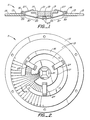
- a membrane-based test probe 11 comprises a membrane 13, a carrier 14, an insulator ring 16, a translation stage 17, a lens assembly 19 and an alignment window 21, as shown in FIGS. 1 and 2.
- Fabricated on membrane 13 are contacts 23 and associated leads 25, shown in FIGS.2 and 3. Contacts 23 are positioned to mate with bonding pads on an integrated circuit die. The electrical functionality of the die can be tested by a circuit analyzer using test probe 11 as an interface.
- the die under test is one of many fabricated on a wafer of silicon or other semiconductor material.
- its center is protruded by translation stage 17 from the plane defined by carrier 15.
- the position of translation stage 17 relative to carrier 15 is maintained by three leaf springs 27.
- Translation stage 17 encircles and maintains the protruded position for the membrane's inner region 29, which bears contacts 23, and the membrane's central region 31, which is radially inward of contacts 23, as shown in FIG. 3.
- Translation stage 17 is used to protrude inner region 29 and central region 31 from their positions prior to translation. Membrane 13 necessarily stretches to accommodate this protrusion. As shown in FIG. 3, translation stage 17 is bonded to membrane 13 with glue 33 along an annular region 35 of membrane 13. Translation stage 17 is considerably less flexible than membrane 13 and thus constrains expansion of regions 29 and 31 enclosed by it. Stretching to accommodate protrusion is thus largely confined to an outer region 37 of membrane 13 between annular region 35 to which translation stage 17 is glued and a peripheral region 39, FIG. 1, of membrane 13 to which carrier 15 is glued.
- contacts 23 formed thereon substantially maintain their original positions during and after the translation procedure. Without such constraint, contacts 23 would not only move, but move in relatively unpredictable amounts since, generally, the elastic deformation forced by the protrusion would be non-uniform.
- FIG. 4 shows a rectangular pattern 41 formed in central region 31.
- This pattern 41 can be formed conveniently in the same steps used in defining leads 25. Being a closed pattern of material more rigid than membrane 13, rectangular pattern 41 serves to further constrain the movement of contacts 23 from the membrane center and relative to each other during protrusion.
- rectangular includes “square” as a special case.
- a central pattern 141 serves a function other than dimensional stability.
- the basically rectangular center pattern 141 comprises two capacitively coupled interdigitated electrical elements 143 and 145.
- Each element 143, 145 has an associated pair of leads 147, 149.
- Element 143 is used as a signal source and its leads 147 are used to provide a sine wave input to pattern 141.
- Element 145 is used as a signal sensor and its lead 149 transmit a detected signal to a signal strength detector (not shown).
- Signal amplitude is at a minimum in the absence of a device under test. As a die is raised toward the contacts, capacitance increases and the detection signal amplitude increases.
- a predetermined signal amplitude threshold can be used to indicate the position of die with respect to probe 11. Thus a signal output by element 145 can be compared with a threshold to determine when a die is properly positioned for electrical testing.
- pattern can be used for alignment of the probe with features on the die other than die bonding pads. This can be helpful when small die bonding pads are obscured by mating contacts to an extent rendering proper registration impracticable.
- Test probe 11 can be manufactured according to the following procedure. First a membrane "blank" is obtained and the desired conductive pattern is formed thereon.
- the membrane material can be purchased or fabricated with a conductive layer on an insulating flexible material, such as polyimide.
- Leads 25 and central pattern 41 can be defined in the conductive layer using photo-lithography.
- a ground plane 51 shown in FIG. 3, can be added, for example, by sputtering a metal onto the side of membrane 13 opposite leads 25.
- contacts 23 holes are drilled into membrane 13 using a laser milling technique. The holes are then filled by plating to form contacts 23.
- Membrane 13 is then bonded to carrier 15. This connection is made using vias plated into holes drilled into membrane 13.
- the carrier conductors are connected to an external contact pad to which test circuitry connects.
- Translation stage 17 can be glued to annular region 35 of the patterned membrane 13. Then translation stage 17 is moved relative to carrier 15 in a direction orthogonal to the plane of membrane 13. As a result of this translation, while outer region 37 assumes a conical form illustrated in FIG. 1. Inner region 29 and central region 31 substantially maintain their forms through the translation. Inner region 29 is slightly articulated due to the force of lens assembly 19 on membrane 13, while central region 31 is essentially planar.
- annular region 35 is glued to the relatively rigid translation stage 17, regions 29 and 31 enclosed thereby are constrained from expanding. Therefore, the additional area required as outer region 37 assumes a conical form is provided primarily by stretching outer region 35 with negligible stretching of inner region 29 and central region 31. Thus, the gluing of translation stage 17 to annular region 35 helps preserve the relative positions of contacts 23 through the translation process.
- Lens assembly 19 includes a self-leveling lens 43 and a disc-shaped elastomeric spring 45.
- the hemispherical shape of self-leveling lens 43 allows it to rotate to maintain gross planarity of elastomeric spring 45 with membrane 13, while the elastomeric spring 45 deforms as necessary to uniformly distribute force over its region of contact with membrane 13.
- the action of lens assembly 19 protrudes central region 31 from inner region 29 so that the latter does not interfere with the mating of contacts 23 with a device under test. Rectangular pattern 41 helps to maintain the relative position of contacts 23 despite the application of force by lens assembly 19.
- rectangular pattern 41 further constrains on the movement of contacts 23 due to the action of translation stage 17.
- rectangular pattern 41 minimizes local non-uniformities that can cause the contacts to move irregularly with respect to each other so that the basic configuration of contacts 23 is not distorted even though a small amount of expansion can occur.
- an improved test probe and method for making the same provide for more precise control of probe contact placement.
- the present invention provides for many alternatives to the preferred embodiments described above.
- the translation stage can take many alternative forms and can be bonded to the membrane using different methods, including gluing, fusing, tacking, and otherwise mechanically attaching.
- the translation stage and membrane carrier can be attached in a variety of ways.
- the central patterns can serve various secondary functions such as alignment, height sensing, etc.
- the fabricating steps can be performed according to a range of techniques and sequences.
Abstract
Description
- The present invention relates to test probes for testing integrated circuits. A major objective of the present invention is to provide a test probe with more precisely controlled contact registration and a method of making the same.
- Semiconductor processing technology has provided for the manufacture of small, complex integrated circuits. These integrated circuits can be processed in batches on a single semiconductor wafer. The cost of fabricating an integrated circuit is low relative to the cost of packaging individual devices and integrating them into systems. Depending on circuit complexity and the processing technology employed, the manufacturing yield for a device can vary considerably, e.g., from 0% to 100% of devices on a wafer may be fully functional.
- Since it is costly to test an integrated circuit after packaging, and even more costly to test after incorporation of a packaged integrated circuit into a system, test instruments have been designed to test integrated circuits while still on the wafers on which they were fabricated. Typically, test probes physically and electrically contact bonding pads on an integrated circuit to provide the electrically coupling required for evaluating its functionality.
- Test probes have had to evolve to keep pace with rapidly advancing integrated circuit technology. Tests probes have been designed with wires cantilevered radially inward and downward to contact bonding pads on an integrated circuit die. Typically, these are the same bonding pads used to couple the die electrically with a package which protects and provides interfacing for the integrated circuit. It has not proved practicable to develop wire-based probes with sufficiently thin and numerous wires to test today's most highly integrated circuits.
- The thin film techniques used to manufacture integrated circuits have been adapted to the fabrication of test probes suitable for more highly integrated circuits. Devices using such techniques or related techniques are disclosed in "Film Supported Probe For The AC Pulse Testing of Integrated Circuits" by F.H. Dill and R.J. Rosalli, IBM Technical Disclosure Bulletin, Vol. 10, No. 10, March 1968, and in U.S. Patent No. 4,636,722 to Adezzone. Contacts can be formed lithographically on a membrane in positions matching the positions of contact pads on a die to be tested. Either before, during, or after contact formation, conductive leads are formed extending from the contact positions radially outward.
- A carrier board can be glued to the membrane. An annular translation stage is positioned within the carrier board and frictionally contacts an annular membrane region enclosing the contacts. The translation stage is pushed against the membrane so that the region enclosed by the translation stage protrudes relative to the carrier board. This ensures that the contacts can contact the bonding pads of the die without physical interference caused by contact of the membrane with areas of the wafer away from the die under test. A lens assembly with an elastomeric spring is pressed against the contact region of the membrane to force the contacts against the pads during testing. A window is situated to confine the lens assembly, pressing it against the membrane, and to provide for visual alignment of contacts and pads.
- While successfully overcoming the limitations of wire-based test probes, available membrane-based test probes have had their capabilities exceeded by further advances in integrated circuit technology. Applicants have found that, as bonding pad size is decreased and as die size is increased, it becomes more difficult to mate die and test probe successfully. Applicants' studies have indicated that one major source of probe-to-die mismatch is the displacement of probe contacts due to elastic deformation of the membrane when the translation stage is protruded from the plane of the carrier board. It is a primary objective of the present invention to overcome these limitations to membrane-based test probes.
- The present invention provides for the constraint of relative movement between contacts during the protrusion of the translation stage. This is done primarily by bonding the translation stage to the membrane so that the membrane region enclosed by the translation stage stretches less than the region outside the translation stage during its protrusion. This approach can be supplemented by forming a rigid pattern within a central region extending near but excluding the contacts on the membrane. This pattern can be dedicated to maintaining contact positions only, or serve an additional purpose such as height sensing or probe alignment. In addition, the contacts can be positioned initially to precompensate for subsequent relative movements.
- These provisions ensure a membrane-based test probe with more precisely controlled contact positions. Since the contact positions can be more accurately matched to the bonding pad positions on a die under test, the mating of probe and die is greatly facilitated. In particular, advanced integrated circuits with increased die sizes and smaller die bonding pads can be tested reliably and conveniently. Other features and advantages of the present invention are apparent in view of the description below with reference to the following drawings.
-
- FIGURE 1 is a sectional view of a test probe in accordance with the present invention.
- FIGURE 2 is a plan view of the test probe of FIG. 1 with portions cutaway.
- FIGURE 3 is a sectional view of a portion of the test probe of FIG.1.
- FIGURE 4 is a plan view of a portion of the test probe of FIG. 1.
- FIGURE 5 is a plan view of a portion of another test probe in accordance with the present invention.
- A membrane-based test probe 11 comprises a
membrane 13, a carrier 14, aninsulator ring 16, atranslation stage 17, alens assembly 19 and analignment window 21, as shown in FIGS. 1 and 2. Fabricated onmembrane 13 arecontacts 23 and associatedleads 25, shown in FIGS.2 and 3.Contacts 23 are positioned to mate with bonding pads on an integrated circuit die. The electrical functionality of the die can be tested by a circuit analyzer using test probe 11 as an interface. - Typically, the die under test is one of many fabricated on a wafer of silicon or other semiconductor material. To ensure probe 11 does not contact adjacent dies, its center is protruded by
translation stage 17 from the plane defined bycarrier 15. The position oftranslation stage 17 relative tocarrier 15 is maintained by threeleaf springs 27.Translation stage 17 encircles and maintains the protruded position for the membrane'sinner region 29, which bearscontacts 23, and the membrane'scentral region 31, which is radially inward ofcontacts 23, as shown in FIG. 3. - During fabrication of probe 11,
contacts 23 andleads 25 are formed whilemembrane 13 is flat.Translation stage 17 is used to protrudeinner region 29 andcentral region 31 from their positions prior to translation.Membrane 13 necessarily stretches to accommodate this protrusion. As shown in FIG. 3,translation stage 17 is bonded tomembrane 13 withglue 33 along anannular region 35 ofmembrane 13.Translation stage 17 is considerably less flexible thanmembrane 13 and thus constrains expansion ofregions outer region 37 ofmembrane 13 betweenannular region 35 to whichtranslation stage 17 is glued and aperipheral region 39, FIG. 1, ofmembrane 13 to whichcarrier 15 is glued. - In reference to FIG. 3, since stretching is minimized in
inner region 29,contacts 23 formed thereon substantially maintain their original positions during and after the translation procedure. Without such constraint,contacts 23 would not only move, but move in relatively unpredictable amounts since, generally, the elastic deformation forced by the protrusion would be non-uniform. - Contact position control can be further enhanced by including a pattern in
central region 31 radially inward fromcontacts 23. FIG. 4 shows arectangular pattern 41 formed incentral region 31. Thispattern 41 can be formed conveniently in the same steps used in definingleads 25. Being a closed pattern of material more rigid thanmembrane 13,rectangular pattern 41 serves to further constrain the movement ofcontacts 23 from the membrane center and relative to each other during protrusion. As used herein, "rectangular" includes "square" as a special case. - In an alternative embodiment, shown in FIG. 5, a
central pattern 141 serves a function other than dimensional stability. The basicallyrectangular center pattern 141 comprises two capacitively coupled interdigitatedelectrical elements element leads Element 143 is used as a signal source and itsleads 147 are used to provide a sine wave input topattern 141.Element 145 is used as a signal sensor and itslead 149 transmit a detected signal to a signal strength detector (not shown). Signal amplitude is at a minimum in the absence of a device under test. As a die is raised toward the contacts, capacitance increases and the detection signal amplitude increases. A predetermined signal amplitude threshold can be used to indicate the position of die with respect to probe 11. Thus a signal output byelement 145 can be compared with a threshold to determine when a die is properly positioned for electrical testing. - In other embodiments, pattern can be used for alignment of the probe with features on the die other than die bonding pads. This can be helpful when small die bonding pads are obscured by mating contacts to an extent rendering proper registration impracticable.
- While gluing of
translation stage 17 and the use of therigid pattern 41 in the central region can limit relative contact displacement sufficiently to allow testing larger and more densely integrated dies than heretofore practicable, these techniques cannot eliminate such displacement entirely. However, these techniques confine stretching to make its efforts predictable. Thus, it becomes practicable to precompensate for the stretching. In other words, the contacts can be fabricated more closely together than required during testing so that, upon protrusion and concomitant stretching,contacts 23 assume the relative positions required for mating even a very large die with very small die bonding pads. - Test probe 11 can be manufactured according to the following procedure. First a membrane "blank" is obtained and the desired conductive pattern is formed thereon. The membrane material can be purchased or fabricated with a conductive layer on an insulating flexible material, such as polyimide. Leads 25 and
central pattern 41 can be defined in the conductive layer using photo-lithography. Aground plane 51, shown in FIG. 3, can be added, for example, by sputtering a metal onto the side ofmembrane 13 opposite leads 25. To formcontacts 23, holes are drilled intomembrane 13 using a laser milling technique. The holes are then filled by plating to formcontacts 23.Membrane 13 is then bonded tocarrier 15. This connection is made using vias plated into holes drilled intomembrane 13. The carrier conductors are connected to an external contact pad to which test circuitry connects. -
Translation stage 17 can be glued toannular region 35 of the patternedmembrane 13. Thentranslation stage 17 is moved relative tocarrier 15 in a direction orthogonal to the plane ofmembrane 13. As a result of this translation, whileouter region 37 assumes a conical form illustrated in FIG. 1.Inner region 29 andcentral region 31 substantially maintain their forms through the translation.Inner region 29 is slightly articulated due to the force oflens assembly 19 onmembrane 13, whilecentral region 31 is essentially planar. - Since
annular region 35 is glued to the relativelyrigid translation stage 17,regions outer region 37 assumes a conical form is provided primarily by stretchingouter region 35 with negligible stretching ofinner region 29 andcentral region 31. Thus, the gluing oftranslation stage 17 toannular region 35 helps preserve the relative positions ofcontacts 23 through the translation process. - Just as the gluing of
translation stage 17 serves to minimize relative contact displacement due to the force of the translation stage onmembrane 13, a centralrectangular pattern 41 can be used to minimize relative displacement ofcontacts 23 due to the force oflens assembly 19.Lens assembly 19 includes a self-levelinglens 43 and a disc-shapedelastomeric spring 45. The hemispherical shape of self-levelinglens 43 allows it to rotate to maintain gross planarity ofelastomeric spring 45 withmembrane 13, while theelastomeric spring 45 deforms as necessary to uniformly distribute force over its region of contact withmembrane 13. The action oflens assembly 19 protrudescentral region 31 frominner region 29 so that the latter does not interfere with the mating ofcontacts 23 with a device under test.Rectangular pattern 41 helps to maintain the relative position ofcontacts 23 despite the application of force bylens assembly 19. - In addition, the mechanical isolation of
regions translation stage 17 is not perfect sorectangular pattern 41 further constrains on the movement ofcontacts 23 due to the action oftranslation stage 17. Specifically,rectangular pattern 41 minimizes local non-uniformities that can cause the contacts to move irregularly with respect to each other so that the basic configuration ofcontacts 23 is not distorted even though a small amount of expansion can occur. - Since a test probe manufactured using the foregoing techniques exhibits predictable contact displacements, these displacements can be precompensated by locating the contacts during patterning a small amount radially inward of the desired ultimate contact positions. As incorporated in the present invention, this isotropic precompensation step is more effective than when applied without the constraining steps. In the case of an unbonded translation stage, local non-uniformities in membrane expansion limit the effectiveness of precompensation because of variable relative contact movements and changes in contact pattern shape.
- In accordance with the foregoing, an improved test probe and method for making the same provide for more precise control of probe contact placement. The present invention provides for many alternatives to the preferred embodiments described above. The translation stage can take many alternative forms and can be bonded to the membrane using different methods, including gluing, fusing, tacking, and otherwise mechanically attaching. The translation stage and membrane carrier can be attached in a variety of ways. The central patterns can serve various secondary functions such as alignment, height sensing, etc. The fabricating steps can be performed according to a range of techniques and sequences. These and other modifications and variations are provided for by the present invention, the scope of which is limited only by the following claims.
Claims (10)
a membrane including an enclosed region, an annular region, an outer region and a peripheral region in radially outward succession;
electrical elements formed on said membrane, said electrical elements including contacts located within said enclosed regions and leads extending from respective ones of said contacts radially outward through said annular region;
a frame bonded to said membrane at said peripheral region;
a translation stage bonded at said annular region of said membrane and enclosing said enclosed region; said
holding means for holding said translation stage in a predetermined position relative to said frame means in a direction perpendicular to said enclosed region so that said enclosed region is deformed to a substantially lesser extent than said outer region.
obtaining a membrane having a central region, an inner region, an annular region, an outer region and a peripheral region in radially outward succession, said regions being mutually exclusive except for common boundaries;
disposing said membrane in a planar configuration including all of said regions;
forming on said membrane contacts and leads so that said leads are electrically coupled to and extending radially outward from respective of said contacts, said contacts being formed on said inner region;
attaching a frame to said peripheral region of said membrane;
bonding a translation stage to said annular region of said membrane; and
moving said translation stage orthogonally with respect to said central region and relative to said frame so the extent of deformation of said membrane in said outer region substantially exceeds the extent of deformation in said central and inner regions.
Applications Claiming Priority (2)
| Application Number | Priority Date | Filing Date | Title |
|---|---|---|---|
| US16276388A | 1988-03-01 | 1988-03-01 | |
| US162763 | 1988-03-01 |
Publications (2)
| Publication Number | Publication Date |
|---|---|
| EP0331282A1 true EP0331282A1 (en) | 1989-09-06 |
| EP0331282B1 EP0331282B1 (en) | 1993-10-13 |
Family
ID=22587042
Family Applications (1)
| Application Number | Title | Priority Date | Filing Date |
|---|---|---|---|
| EP19890300688 Expired - Lifetime EP0331282B1 (en) | 1988-03-01 | 1989-01-25 | Membrane-based ic test probe with precisely positioned contacts |
Country Status (3)
| Country | Link |
|---|---|
| EP (1) | EP0331282B1 (en) |
| JP (1) | JPH01269065A (en) |
| DE (1) | DE68909811D1 (en) |
Cited By (14)
| Publication number | Priority date | Publication date | Assignee | Title |
|---|---|---|---|---|
| EP0360396A2 (en) * | 1988-09-23 | 1990-03-28 | Hewlett-Packard Company | Force delivery system for improved precision membrane probe |
| EP0425744A1 (en) * | 1989-11-02 | 1991-05-08 | Hewlett-Packard Company | Membrane probe with automatic contact scrub action |
| GB2239744A (en) * | 1989-11-07 | 1991-07-10 | Sharp Kk | Testing L.C.D. displays; flexible test circuit contacts |
| EP0454347A2 (en) * | 1990-04-24 | 1991-10-30 | John Fluke Mfg. Co., Inc. | Vacuum-actuated test fixture for testing electronic components |
| US5180977A (en) * | 1991-12-02 | 1993-01-19 | Hoya Corporation Usa | Membrane probe contact bump compliancy system |
| EP0532925A1 (en) * | 1991-08-26 | 1993-03-24 | Hughes Aircraft Company | Rigid-flex circuits with raised features as IC test probes |
| EP0613013A1 (en) * | 1993-02-25 | 1994-08-31 | Hughes Aircraft Company | Self leveling membrane test probe |
| EP0623826A1 (en) * | 1993-04-29 | 1994-11-09 | Hughes Aircraft Company | Membrane connector with stretch induced micro scrub |
| US5621333A (en) * | 1995-05-19 | 1997-04-15 | Microconnect, Inc. | Contact device for making connection to an electronic circuit device |
| US5933018A (en) * | 1995-08-29 | 1999-08-03 | Shin-Etsu Polymer Co., Ltd. | Liquid crystal display panel inspection device and method for manufacturing same |
| US6046599A (en) * | 1996-05-20 | 2000-04-04 | Microconnect, Inc. | Method and device for making connection |
| US6343369B1 (en) | 1998-09-15 | 2002-01-29 | Microconnect, Inc. | Methods for making contact device for making connection to an electronic circuit device and methods of using the same |
| US6496026B1 (en) | 2000-02-25 | 2002-12-17 | Microconnect, Inc. | Method of manufacturing and testing an electronic device using a contact device having fingers and a mechanical ground |
| CN109655737A (en) * | 2018-12-24 | 2019-04-19 | 北京华峰测控技术股份有限公司 | A kind of test method of wafer |
Families Citing this family (5)
| Publication number | Priority date | Publication date | Assignee | Title |
|---|---|---|---|---|
| US20020053734A1 (en) | 1993-11-16 | 2002-05-09 | Formfactor, Inc. | Probe card assembly and kit, and methods of making same |
| US8033838B2 (en) | 1996-02-21 | 2011-10-11 | Formfactor, Inc. | Microelectronic contact structure |
| KR100675487B1 (en) * | 2005-06-02 | 2007-01-30 | 주식회사 파이컴 | Probe card |
| DE102005054593B4 (en) * | 2005-11-14 | 2018-04-26 | Immobiliengesellschaft Helmut Fischer Gmbh & Co. Kg | Measuring probe for measuring the thickness of thin layers |
| US7764076B2 (en) | 2007-02-20 | 2010-07-27 | Centipede Systems, Inc. | Method and apparatus for aligning and/or leveling a test head |
Citations (3)
| Publication number | Priority date | Publication date | Assignee | Title |
|---|---|---|---|---|
| US4065717A (en) * | 1970-09-15 | 1977-12-27 | Signetics Corporation | Multi-point microprobe for testing integrated circuits |
| US4649339A (en) * | 1984-04-25 | 1987-03-10 | Honeywell Inc. | Integrated circuit interface |
| EP0226995A2 (en) * | 1985-12-23 | 1987-07-01 | Tektronix, Inc. | Multiple lead probe for integrated circuits |
-
1989
- 1989-01-25 DE DE89300688T patent/DE68909811D1/en not_active Expired - Lifetime
- 1989-01-25 EP EP19890300688 patent/EP0331282B1/en not_active Expired - Lifetime
- 1989-03-01 JP JP1049740A patent/JPH01269065A/en active Pending
Patent Citations (3)
| Publication number | Priority date | Publication date | Assignee | Title |
|---|---|---|---|---|
| US4065717A (en) * | 1970-09-15 | 1977-12-27 | Signetics Corporation | Multi-point microprobe for testing integrated circuits |
| US4649339A (en) * | 1984-04-25 | 1987-03-10 | Honeywell Inc. | Integrated circuit interface |
| EP0226995A2 (en) * | 1985-12-23 | 1987-07-01 | Tektronix, Inc. | Multiple lead probe for integrated circuits |
Cited By (25)
| Publication number | Priority date | Publication date | Assignee | Title |
|---|---|---|---|---|
| EP0360396A2 (en) * | 1988-09-23 | 1990-03-28 | Hewlett-Packard Company | Force delivery system for improved precision membrane probe |
| EP0360396A3 (en) * | 1988-09-23 | 1991-02-06 | Hewlett-Packard Company | Force delivery system for improved precision membrane probe |
| EP0425744A1 (en) * | 1989-11-02 | 1991-05-08 | Hewlett-Packard Company | Membrane probe with automatic contact scrub action |
| GB2239744A (en) * | 1989-11-07 | 1991-07-10 | Sharp Kk | Testing L.C.D. displays; flexible test circuit contacts |
| GB2239744B (en) * | 1989-11-07 | 1994-03-16 | Sharp Kk | Tester head |
| EP0454347A2 (en) * | 1990-04-24 | 1991-10-30 | John Fluke Mfg. Co., Inc. | Vacuum-actuated test fixture for testing electronic components |
| EP0454347A3 (en) * | 1990-04-24 | 1992-05-20 | John Fluke Mfg. Co., Inc. | Vacuum-actuated test fixture for testing electronic components |
| EP0532925A1 (en) * | 1991-08-26 | 1993-03-24 | Hughes Aircraft Company | Rigid-flex circuits with raised features as IC test probes |
| US5180977A (en) * | 1991-12-02 | 1993-01-19 | Hoya Corporation Usa | Membrane probe contact bump compliancy system |
| EP0613013A1 (en) * | 1993-02-25 | 1994-08-31 | Hughes Aircraft Company | Self leveling membrane test probe |
| EP0623826A1 (en) * | 1993-04-29 | 1994-11-09 | Hughes Aircraft Company | Membrane connector with stretch induced micro scrub |
| US5395253A (en) * | 1993-04-29 | 1995-03-07 | Hughes Aircraft Company | Membrane connector with stretch induced micro scrub |
| US5621333A (en) * | 1995-05-19 | 1997-04-15 | Microconnect, Inc. | Contact device for making connection to an electronic circuit device |
| US6091256A (en) * | 1995-05-19 | 2000-07-18 | Microconnect, Inc. | Contact device for making connection to an electronic circuit device |
| US5933018A (en) * | 1995-08-29 | 1999-08-03 | Shin-Etsu Polymer Co., Ltd. | Liquid crystal display panel inspection device and method for manufacturing same |
| US6046599A (en) * | 1996-05-20 | 2000-04-04 | Microconnect, Inc. | Method and device for making connection |
| US6343369B1 (en) | 1998-09-15 | 2002-01-29 | Microconnect, Inc. | Methods for making contact device for making connection to an electronic circuit device and methods of using the same |
| US6622289B2 (en) | 1998-09-15 | 2003-09-16 | Microconnect, Llc | Methods for making contact device for making connection to an electronic circuit device and methods of using the same |
| US6957405B2 (en) | 1998-09-15 | 2005-10-18 | Microconnect Llc | Methods for manufacturing an electronic device having an electronically determined physical test member |
| US7386816B2 (en) | 1998-09-15 | 2008-06-10 | Microconnect Llc | Method for manufacturing an electronic device having an electronically determined physical test member |
| US8056031B2 (en) | 1998-09-15 | 2011-11-08 | Microconnect Corp. | Methods for manufacturing an electronic device using an electronically determined test member |
| US8756537B2 (en) | 1998-09-15 | 2014-06-17 | Microconnect Corp. | Methods for making contact device for making connection to an electronic circuit device and methods using the same |
| US6496026B1 (en) | 2000-02-25 | 2002-12-17 | Microconnect, Inc. | Method of manufacturing and testing an electronic device using a contact device having fingers and a mechanical ground |
| CN109655737A (en) * | 2018-12-24 | 2019-04-19 | 北京华峰测控技术股份有限公司 | A kind of test method of wafer |
| CN109655737B (en) * | 2018-12-24 | 2020-11-27 | 北京华峰测控技术股份有限公司 | Wafer testing method |
Also Published As
| Publication number | Publication date |
|---|---|
| EP0331282B1 (en) | 1993-10-13 |
| DE68909811D1 (en) | 1993-11-18 |
| JPH01269065A (en) | 1989-10-26 |
Similar Documents
| Publication | Publication Date | Title |
|---|---|---|
| EP0331282B1 (en) | Membrane-based ic test probe with precisely positioned contacts | |
| US4980637A (en) | Force delivery system for improved precision membrane probe | |
| US7570069B2 (en) | Resilient contact probes | |
| JP4389209B2 (en) | Interconnect assembly for printed circuit board and manufacturing method | |
| KR100430208B1 (en) | Test assembly | |
| US5189363A (en) | Integrated circuit testing system having a cantilevered contact lead probe pattern mounted on a flexible tape for interconnecting an integrated circuit to a tester | |
| US5629630A (en) | Semiconductor wafer contact system and method for contacting a semiconductor wafer | |
| US5059898A (en) | Wafer probe with transparent loading member | |
| JPH04266043A (en) | Apparatus and method for test of integrated circuit | |
| US5773986A (en) | Semiconductor wafer contact system and method for contacting a semiconductor wafer | |
| US6307394B1 (en) | Test carrier with variable force applying mechanism for testing semiconductor components | |
| EP0298219A2 (en) | Method and apparatus for testing unpackaged integrated circuits in a hybrid circuit environment | |
| JPS6325564A (en) | Catalytic device for device to be inspected of microelectronics | |
| US5369358A (en) | Method of ensuring electrical contact between test probes and chip pads through the use of vibration and nondestructive deformation | |
| US5500604A (en) | Radial tensioning lamination fixture for membrane test probe | |
| JP3497748B2 (en) | Inspection method for semiconductor integrated circuit | |
| KR20220091186A (en) | Probe Card | |
| JPH087234B2 (en) | Test probe equipment | |
| JPH07302821A (en) | Integrated circuit testing device | |
| JP2679684B2 (en) | Anisotropic conductive film and semiconductor wafer measuring jig using anisotropic conductive film | |
| US6720574B2 (en) | Method of testing a semiconductor chip | |
| KR100446551B1 (en) | Volcano type probe, its manufacturing method and probe card having it | |
| JP2001201516A (en) | Manufacturing method and device of probe element and hollow forming device | |
| JPH0792477B2 (en) | Probe card | |
| JP2000002718A (en) | Probe device |
Legal Events
| Date | Code | Title | Description |
|---|---|---|---|
| PUAI | Public reference made under article 153(3) epc to a published international application that has entered the european phase |
Free format text: ORIGINAL CODE: 0009012 |
|
| AK | Designated contracting states |
Kind code of ref document: A1 Designated state(s): DE FR GB |
|
| 17P | Request for examination filed |
Effective date: 19891023 |
|
| 17Q | First examination report despatched |
Effective date: 19911216 |
|
| GRAA | (expected) grant |
Free format text: ORIGINAL CODE: 0009210 |
|
| AK | Designated contracting states |
Kind code of ref document: B1 Designated state(s): DE FR GB |
|
| PG25 | Lapsed in a contracting state [announced via postgrant information from national office to epo] |
Ref country code: FR Effective date: 19931013 Ref country code: DE Effective date: 19931013 |
|
| REF | Corresponds to: |
Ref document number: 68909811 Country of ref document: DE Date of ref document: 19931118 |
|
| PG25 | Lapsed in a contracting state [announced via postgrant information from national office to epo] |
Ref country code: GB Effective date: 19940125 |
|
| EN | Fr: translation not filed | ||
| PLBE | No opposition filed within time limit |
Free format text: ORIGINAL CODE: 0009261 |
|
| STAA | Information on the status of an ep patent application or granted ep patent |
Free format text: STATUS: NO OPPOSITION FILED WITHIN TIME LIMIT |
|
| GBPC | Gb: european patent ceased through non-payment of renewal fee |
Effective date: 19940125 |
|
| 26N | No opposition filed |