EP0335104A2 - Vorrichtung zum optischen Verbinden eines oder mehrerer optischer Sender mit einem oder mehreren optischen Detektoren eines oder mehrerer integrierter Schaltkreise - Google Patents
Vorrichtung zum optischen Verbinden eines oder mehrerer optischer Sender mit einem oder mehreren optischen Detektoren eines oder mehrerer integrierter Schaltkreise Download PDFInfo
- Publication number
- EP0335104A2 EP0335104A2 EP89103004A EP89103004A EP0335104A2 EP 0335104 A2 EP0335104 A2 EP 0335104A2 EP 89103004 A EP89103004 A EP 89103004A EP 89103004 A EP89103004 A EP 89103004A EP 0335104 A2 EP0335104 A2 EP 0335104A2
- Authority
- EP
- European Patent Office
- Prior art keywords
- optical
- wst
- spacer
- light
- waveguide
- Prior art date
- Legal status (The legal status is an assumption and is not a legal conclusion. Google has not performed a legal analysis and makes no representation as to the accuracy of the status listed.)
- Withdrawn
Links
Images

Classifications
-
- G—PHYSICS
- G02—OPTICS
- G02B—OPTICAL ELEMENTS, SYSTEMS OR APPARATUS
- G02B6/00—Light guides; Structural details of arrangements comprising light guides and other optical elements, e.g. couplings
- G02B6/24—Coupling light guides
- G02B6/42—Coupling light guides with opto-electronic elements
- G02B6/43—Arrangements comprising a plurality of opto-electronic elements and associated optical interconnections
-
- H—ELECTRICITY
- H04—ELECTRIC COMMUNICATION TECHNIQUE
- H04B—TRANSMISSION
- H04B10/00—Transmission systems employing electromagnetic waves other than radio-waves, e.g. infrared, visible or ultraviolet light, or employing corpuscular radiation, e.g. quantum communication
- H04B10/80—Optical aspects relating to the use of optical transmission for specific applications, not provided for in groups H04B10/03 - H04B10/70, e.g. optical power feeding or optical transmission through water
- H04B10/801—Optical aspects relating to the use of optical transmission for specific applications, not provided for in groups H04B10/03 - H04B10/70, e.g. optical power feeding or optical transmission through water using optical interconnects, e.g. light coupled isolators, circuit board interconnections
-
- H—ELECTRICITY
- H01—ELECTRIC ELEMENTS
- H01L—SEMICONDUCTOR DEVICES NOT COVERED BY CLASS H10
- H01L2224/00—Indexing scheme for arrangements for connecting or disconnecting semiconductor or solid-state bodies and methods related thereto as covered by H01L24/00
- H01L2224/01—Means for bonding being attached to, or being formed on, the surface to be connected, e.g. chip-to-package, die-attach, "first-level" interconnects; Manufacturing methods related thereto
- H01L2224/42—Wire connectors; Manufacturing methods related thereto
- H01L2224/47—Structure, shape, material or disposition of the wire connectors after the connecting process
- H01L2224/48—Structure, shape, material or disposition of the wire connectors after the connecting process of an individual wire connector
- H01L2224/4805—Shape
- H01L2224/4809—Loop shape
- H01L2224/48091—Arched
-
- H—ELECTRICITY
- H01—ELECTRIC ELEMENTS
- H01L—SEMICONDUCTOR DEVICES NOT COVERED BY CLASS H10
- H01L2224/00—Indexing scheme for arrangements for connecting or disconnecting semiconductor or solid-state bodies and methods related thereto as covered by H01L24/00
- H01L2224/01—Means for bonding being attached to, or being formed on, the surface to be connected, e.g. chip-to-package, die-attach, "first-level" interconnects; Manufacturing methods related thereto
- H01L2224/42—Wire connectors; Manufacturing methods related thereto
- H01L2224/47—Structure, shape, material or disposition of the wire connectors after the connecting process
- H01L2224/48—Structure, shape, material or disposition of the wire connectors after the connecting process of an individual wire connector
- H01L2224/481—Disposition
- H01L2224/48135—Connecting between different semiconductor or solid-state bodies, i.e. chip-to-chip
- H01L2224/48137—Connecting between different semiconductor or solid-state bodies, i.e. chip-to-chip the bodies being arranged next to each other, e.g. on a common substrate
Definitions
- the invention relates to a device for optically connecting one or more optical transmitters to one or more optical detectors of one or more integrated circuits.
- an optical device for Feeding the light emitted by an optical transmitter to a plurality of optical detectors consists of a hologram which is arranged above the transmitter and the integrated circuit, to which the light emitted by a transmitter is fed, and which this light is directed to certain optical detectors on the integrated Circuit distributed.
- This publication does not provide any details about the fixing of the detectors, the hologram and the integrated circuit relative to one another.
- the silicon specified in claim 3 being particularly advantageous because this material is anisotropically etchable and therefore simple to manufacture of inclined side surfaces required in certain embodiments of the invention.
- a particularly expedient embodiment of the spacer of the device according to the invention which can be produced easily and with high accuracy using conventional lithographic processes and, moreover, can be used universally, is evident from claim 4.
- an embodiment of the device according to the invention is advantageous.
- the waveguide structure specified there preferably consists of one or more strip waveguides, which advantageously consist of glass according to claim 7, because then the structure can be etched out very easily with the aid of a conventional lithographic process from a glass layer which is also easy to produce.
- optical transmitters and optical detectors can be carried out in various ways, with preferred options arising from claims 8 to 16.
- a recess in the cover body is necessary.
- a recess in the cover body which can consist of a window-like opening, can also be provided in other embodiments in which all of the components fixed on the substrate are lower than the spacer, so that a recess in the cover body would not be necessary.
- Claim 17 is specifically directed to the novel device for forming external optical connections, which is advantageously designed as specified in claim 18.
- external optical connections which is advantageously designed as specified in claim 18.
- internal optical connections can also be implemented in a simple manner at the same time.
- the devices according to claims 19 to 21 are particularly suitable for a device according to claim 18 if external and internal connections between and in integrated circuits are to be made simultaneously.
- the substrate Su, the spacer Ah and the cover body DK each consist of a layer of silicon, the layer thickness of which is, for example, 300 ⁇ m to 1000 ⁇ m.
- a silicon chip with an integrated circuit IC is arranged on the substrate Su on both sides of the spacer Ah, with an optical transmitter oS in the form of a laser diode array running perpendicular to the plane of the drawing and assigned to the integrated circuit IC arranged on this side on the right side an optical detector oD assigned to the integrated circuit IC arranged on this other side is arranged on the substrate Su in the form of a photodetector array running perpendicular to the plane of the drawing.
- optical transmitter oS electrically connected to the associated integrated circuit IC is controlled by this circuit, while the optical detector oD is electrically connected to the integrated circuit IC assigned to it and controls it.
- the optical transmitters oS and optical detectors oD are separate components from the semiconductor chips. However, they could also be integrated on the chips, as is the case with the detectors oD in FIG. 3.
- the spacer Ah is expediently a layer in which areas Be are recessed, in which the building blocks are fixed on the substrate Su, for example by gluing. These areas Be can be easily manufactured by etching.
- the spacer Ah is covered by the cover body DK.
- a waveguide structure Wst is arranged between the cover body DK and the spacer Ah, which can consist, for example, of parallel strip waveguides made of glass, each of which leads from a laser diode of the optical transmitter oS to an assigned photodetector of the optical detector oD.
- This waveguide structure Wst can be produced in a simple manner in that a glass layer of, for example, a thickness of 8 ⁇ m to 50 ⁇ m is applied to the spacer Ah or the cover body DK and the desired waveguide structure Wst is etched from this layer using a conventional photolithographic process .
- the glass layer can be applied, for example, using a known CVD method. The production of the waveguide structure Wst is therefore simple and unproblematic.
- the optical transmitter oS emits its light in the plane of the strip waveguide structure Wst.
- the light-emitting area eB of this transmitter oS lies opposite an end face Stf of a waveguide of the strip waveguide structure Wst, through which the light emitted by the transmitter oS is coupled into the waveguide structure Wst.
- a base Sm can be used which is suitably dimensioned and on which the transmitter oS is fastened.
- a recess Asp is provided in the area of the optical transmitter, into which these parts T project.
- This cutout Asp can be formed, for example, in the form of a window in the cover body and can be produced by etching, for example by preferential etching of silicon.
- Such recesses Asp can, however, also be provided at other locations on the cover body DK, for example wherever modules with integrated circuits are fixed on the substrate Su.
- the optical detector oD is coupled via a deflecting element Ue3, which the light coupled out through an end face Stf of a waveguide of the waveguide structure Wst to a detector window ster Df deflected, which is facing the cover body DK.
- This deflection element Ue3 can consist, for example, of an oblique end face of a short waveguide section Wa, which is fixed on the underside of the cover body DK so that the light from the waveguide structure Wst falls on the oblique end face.
- the optical detector oD could also be arranged such that its detector window Df faces an end face Stf of a waveguide of the waveguide structure Wst and the light coupled out through this end face is fed directly to the detector window Df.
- the recess Asp provided on the detector side in the embodiment according to FIG. 1 would be indispensable.
- the thickness of the spacer Ah can be made greater than the maximum height of the modules attached to the substrate, for example by gluing. In this case, cutouts in the cover body DK are not necessary.
- FIG. 2 shows such an embodiment, in which the coupling and uncoupling is carried out by deflection.
- This embodiment according to FIG. 2 differs from the embodiment according to FIG. 1 only in that the light is also coupled into the waveguide structure Wst by deflection and in that no cutouts are provided in the cover body DK.
- the light emitted by the optical transmitter oS parallel to the plane of the waveguide structure Wst and divergent is concentrated by a converging lens Li and two deflection elements Ue1 and Ue2 on an end face Stf of a waveguide of the waveguide structure Wst.
- the lens Li which can be fastened on a base which is fixed on the substrate Su and which is not shown, can be a glass rod with a circular cross section arranged with its longitudinal direction perpendicular to the plane of the drawing.
- the first deflection element Ue1 expediently consists of an oblique screen th surface of the spacer Ah, which deflects the light towards the other deflecting element Ue2.
- the inclined side surface can be produced by anisotropic etching of the silicon layer forming the spacer Ah.
- the other deflection element Ue2 is formed by an oblique end face of a short waveguide section Wa, which is fastened to the underside of the cover body DK in such a way that the oblique end face Ue2 deflects the incoming light onto the end face Stf of the waveguide of the waveguide structure Wst.
- the spacer Ah consists of two silicon layers Sch1 and Sch2.
- the lower silicon layer Sch1 has an inclined side surface serving as a deflection element Ue, which can be produced by anisotropic etching.
- the light emitted by the optical transmitter oS for example a laser diode, in the direction of the deflection element Ue is deflected by this deflection element Ue to a light distribution device Hol which is attached or formed on the underside of the cover body DK and which distributes the supplied light to optical detectors oD, which are integrated on a semiconductor chip with an integrated circuit IC, for example in the form of photo detectors.
- the light distribution device Hol can be a hologram, for example.
- the embodiment according to FIG. 3 has the advantage that it is compatible with the embodiments according to FIGS. 1 and 2.
- FIGS. 4 and 5 show an embodiment in which both the optical connection according to FIGS. 1 and 2 and the optical connection according to FIG. 3 are realized on the same substrate Su.
- the substrate Su consists of a silicon wafer on which a first layer Sch1 of the spacer Ah is fixed, in which rectangular areas Be are recessed.
- a semiconductor chip with an integrated circuit IC and an optical transmitter oS is arranged in each rectangular area Be.
- There is also one on this layer Sch1 Strip waveguide structure Wst is formed, the waveguide of which transmits the light emitted by an optical transmitter oS of a clock generator TG to optical detectors oD of the various integrated circuits IC.
- FIG. 5 shows a top view of the layer Sch1 with the waveguide structure Wst.
- the side surfaces of the recessed areas Be of the first layer Sch1 are oblique so that they can form deflection elements Ue.
- a second layer Sch2 of the spacer Ah is applied to the waveguide structure Wst, which has recessed areas Be which coincide with the recessed areas Be of the first layer Sch1.
- the cover body DK is applied to the second layer Sch2.
- a light distribution element Hol is attached to the underside of the cover body DK, so that an optical connection according to FIG. 3 is implemented in each area.
- the recessed areas Be can be produced with high accuracy by etching or anisotropically etching silicon wafers. Since the same material is used for all layers, no thermal stresses occur.
- the substrate Su, the spacer Ah and the cover body DK can be fixed relative to one another, for example, by gluing them together or by screwing them together.
Landscapes
- Physics & Mathematics (AREA)
- General Physics & Mathematics (AREA)
- Optics & Photonics (AREA)
- Electromagnetism (AREA)
- Engineering & Computer Science (AREA)
- Computer Networks & Wireless Communication (AREA)
- Signal Processing (AREA)
- Optical Couplings Of Light Guides (AREA)
- Photo Coupler, Interrupter, Optical-To-Optical Conversion Devices (AREA)
- Optical Communication System (AREA)
- Optical Integrated Circuits (AREA)
Abstract
Description
- Die Erfindung betrifft eine Vorrichtung zum optischen Verbinden eines oder mehrerer optischer Sender mit einem oder mehreren optischen Detektoren eines oder mehrerer integrierter Schaltkreise.
- Aus Appl. Optics, Vol. 26, Nr. 20, 15. Okt. 1987, S. 4377-4384 ist eine Vorrichtung zum optischen Verbinden mehrerer, einem gemeinsamen integrierten Schaltkreis zugeordneter optischer Sender mit mehreren optischen Detektoren dieses Schaltkreises bekannt, bei dem eine optische Einrichtung zum Zuleiten des von einem optischen Sender ausgesandten Lichts zu mehreren optischen Detektoren aus einem Hologramm besteht, das oberhalb der Sender und dem integrierten Schaltkreis angeordnet ist, dem das von einem Sender ausgesandte Licht zugeleitet ist, und das dieses zugeleitete Licht auf bestimmte optische Detektoren auf dem integrierten Schaltkreis verteilt. Näheres über die Fixierung der Detektoren, des Hologramms und des integrierten Schaltkreises relativ zueinander geht aus dieser Druckschrift nicht hervor.
- Aus Appl. Optics, Vol. 26, Nr. 17, 1. Sept. 1987, S. 3649-3654 ist eine Vorrichtung zum optischen Verbinden mehrerer optischer Sender mit mehreren optischen Detektoren bekannt, bei der die optischen Sender auf einem Substrat angeordnet und von einer transparenten, schichtförmigen Ausrichtungsschablone abgedeckt sind. Zwischen dieser Schablone und einer Schicht aus Silizium ist als eine optische Einrichtung zum Zuleiten des von einem optischen Sender ausgesandten Lichts zu einem oder mehreren optischen Detektoren eine Fresnelsche Phasenplattenlinse angeordnet, durch die das von den optischen Sendern ausgesandte Licht, das die Schablone und die Schicht aus Silizium Ed 1 Sti/30.03.1988 durchsetzt, den optischen Detektoren zugeleitet ist, die auf der Schicht aus Silizium auf der von der Linse und den Sendern abgekehrten Seite angeordnet sind.
- Aufgabe der vorliegenden Erfindung ist es, eine Vorrichtung zum optischen Verbinden eines oder mehrerer optischer Sender mit einem oder mehreren optischen Detektoren eines oder mehrerer integrierter Schaltkreise zu schaffen, bei welchem mit möglichst wenig baulichem Aufwand und mit großer Präzision sowohl externe optische Verbindungen von verschiedenen integrierten Schaltkreisen, insbesondere von Rechnerchips, als auch interne optische Verbindungen bei einzelnen integrierten Schaltkreisen sowie solche externen und internen optischen Verbindungen in Kombination herstellbar sind.
- Diese Aufgabe wird durch die im Anspruch 1 angegebenen Merkmale gelöst.
- Durch diese Lösung können mit im wesentlichen nur drei Bauelementen interne und externe optische Verbindungen in oder zwischen integrierten Halbleiterchips auf einfache Weise und mit hoher Präzision hergestellt werden, wobei ein besonderer Vorteil darin besteht, daß externe und interne optische Verbindungen in Kombination hergestellt werden können.
- Damit die erzielbare hohe Präzision dauerhaft bleibt, ist es zweckmäßig, die erfindungsgemäße Vorrichtung so zu gestalten, wie es im Anspruch 2 angegeben ist, wobei das im Anspruch 3 angegebene Silizium von besonderem Vorteil ist, weil dieses Material anisotrop ätzbar ist und dadurch eine einfache Herstellung von schrägen Seitenflächen ermöglicht, die bei bestimmten Ausführungsformen der Erfindung erforderlich sind.
- Eine besonders zweckmäßige Ausgestaltung des Abstandshalters der erfindungsgemäßen Vorrichtung, der mit herkömmlichen lithografischen Verfahren einfach und mit hoher Genauigkeit herstellbar und darüber hinaus universell einsetzbar ist, geht aus dem Anspruch 4 hervor.
- Für die Herstellung externer optischer Verbindungen zwischen verschiedenen optischen Schaltkreisen, beispielsweise zwischen Rechnerchips zur Ermöglichung eines Datenaustausches zwischen diesen Chips, ist eine Ausgestaltung der erfindungsgemäßen Vorrichtung vorteilhaft, die im Anspruch 5 angegeben ist.
- Die dort angegebene Wellenleiterstruktur besteht bevorzugterweise gemäß Anspruch 6 aus einem oder mehreren Streifenwellenleitern, die vorteilhafterweise gemäß Anspruch 7 aus Glas bestehen, weil dann die Struktur sehr einfach mit Hilfe eines herkömmlichen lithografischen Prozesses aus einer ebenfalls einfach herstellbaren Glasschicht herausgeätzt werden kann.
- Die Ankopplung optischer Sender und optischer Detektoren an die Wellenleiterstruktur kann auf verschiedene Weise vorgenommen werdne, wobei bevorzgute Möglichkeiten aus den Ansprüche 8 bis 16 hervorgehen.
- Bei den im Anspruch 9 und im Anspruch 14 angegebenen Ausführungsformen ist eine Aussparung im Deckkörper notwendig. Eine solche Aussparung im Deckkörper, die in einer fensterartigen Öffnung bestehen kann, kann aber auch bei anderen Ausführungsformen vorgesehen sein, bei denen alle auf dem Substrat fixierten Bausteine niedriger als der Abstandshalter sind, so daß eine Aussparung im Deckkörper nicht erforderlich wäre.
- Der Anspruch 17 ist konkret auf die neuartige Vorrichtung zur Bildung externer optischer Verbindungen gerichtet, die vorteilhafterweise so ausgestaltet ist, wie es im Anspruch 18 angegeben ist. Gerade bei dieser letztgenannten Vorrichtung können neben den externen optischen Verbindungen auf einfache Weise auch interne optische Verbindungen gleichzeitig realisiert werden.
- Eine solche interne optische Verbindung ist bei einer erfindungsgemäßen Vorrichtung zweckmäßigerweise so ausgebildet, wie es im Anspruch 19 angegeben ist. Bevorzugte Ausgestaltungen dieser Vorrichtung gehen aus den Ansprüchen 20 und 21 hervor.
- Die Vorrichtungen nach den Ansprüchen 19 bis 21 sind insbesondere für eine Vorrichtung nach Anspruch 18 geeignet, wenn externe und interne Verbindungen zwischen und in integrierten Schaltkreisen gleichzeitig herzustellen sind.
- Eine vorteilhafte Vorrichtung, bei welcher externe und interne optische Verbindungen realisiert oder realisierbar sind, geht aus dem Anspruch 22 hervor.
- Die Erfindung wird anhand der Figuren in der nun folgenden Beschreibung beispielhaft näher erläutert. Von den Figuren zeigen:
- Figur 1 einen Schnitt durch eine Ausführungsform einer Vorrichtung, bei welcher zwei Silizium-Chips mit integrierten Schaltkreisen durch eine optische Parallelverbindung extern miteinander verbunden sind,
- Figur 2 einen Schnitt durch eine andere Ausführungsform der Vorrichtung nach Figur 1,
- Figur 3 einen Schnitt durch eine Ausführungsform einer Vorrichtung, bei welcher ein optischer Detektor, der einem Silizium-Chip mit einer integrierten Schaltung zugeordnet ist, optisch mit Detektoren dieses Chips verbunden ist, so daß eine interne optische Verbindung gegeben ist,
- Figur 4 einen Schnitt durch eine Ausführungsform einer Vorrichtung, bei welcher Silizium-Chips mit integrierten Schaltkreisen extern optisch verbunden sind, und bei welcher für jeden Chip auch eine interne optische Verbindung realisiert ist, und
- Figur 5 eine Draufsicht auf die Ausführungsform nach Figur 4, wobei der Deckkörper und eine Schicht des Abstandshalters weggelassen sind.
- In den Figuren sind gleiche oder einander entsprechende Teile mit gleichen Bezugszeichen versehen.
- Bei der Ausführungsform nach Figur 1 bestehen das Substrat Su, der Abstandshalter Ah und der Deckkörper DK jeweils aus einer Schicht aus Silizium, deren Schichtdicke beispielsweise 300 µm bis 1000 µm beträgt. Auf dem Substrat Su sind zu beiden Seiten des Abstandshalters Ah jeweils ein Silizium-Chip mit einem integrierten Schaltkreis IC angeordnet, wobei auf der linken Seite ein dem auf dieser Seite angeordneten integrierten Schaltkreis IC zugeordneter optischer Sender oS in Form eines senkrecht zur Zeichenebene verlaufenden Laserdiodenarrays und auf der rechten Seite ein dem auf dieser anderen Seite angeordneten integrierten Schaltkreis IC zugeordneter optischer Detektor oD in Form eines senkrecht zur Zeichenebene verlaufenden Fotodetektorarrays auf dem Substrat Su angeordnet ist. Der mit dem zugeordneten integrierten Schaltkreis IC elektrisch verbundene optische Sender oS wird von diesem Schaltkreis gesteuert, während der optische Detektor oD elektrisch mit dem ihm zugeordneten integrierten Schaltkreis IC verbunden ist und diesen steuert. In der Figur 1 sind wie in den Figuren 2, 4 und 5 die optischen Sender oS und optischen Detektoren oD von den Halbleiterchips getrennte Bausteine. Sie könnten aber auch mit auf den Chips integriert sein, so wie es bei den Detektoren oD der Figur 3 der Fall ist.
- Der Abstandshalter Ah ist zweckmäßigerweise eine Schicht, in der Bereiche Be ausgespart sind, in denen die Bausteine auf dem Substrat Su fixiert sind, beispielsweise durch Kleben. Diese Bereiche Be können leicht durch Ätzen hergestellt werden.
- Der Abstandshalter Ah ist von dem Deckkörper DK abgedeckt. Zwischen dem Deckkörper DK und dem Abstandshalter Ah ist eine Wellenleiterstruktur Wst angeordnet, die beispielsweise aus parallelen Streifenwellenleitern aus Glas bestehen kann, von denen jeder von einer Laserdiode des optischen Senders oS zu einem zugeordneten Fotodetektor des optischen Detektors oD führt.
- Diese Wellenleiterstruktur Wst kann auf einfache Weise dadurch hergestellt werden, daß auf den Abstandshalter Ah oder den Deckkörper DK eine Glasschicht von beispielsweise einer Dicke von 8 µm bis 50 µm aufgebracht wird und aus dieser Schicht mit Hilfe eines herkömmlichen fotolithografischen Prozesses die gewünschte Wellenleiterstruktur Wst geätzt wird. Das Anbringen der Glasschicht kann beispielsweise mit Hilfe eines bekannten CVD-Verfahrens erfolgen. Die Herstellung der Wellenleiterstruktur Wst ist somit einfach und unproblematisch.
- Das Ein- und Auskoppeln von Licht in oder aus der Wellenleiterstruktur Wst kann auf verschiedene Weise erfolgen. Bei der Ausführungsform nach Figur 1 strahlt der optische Sender oS sein Licht in der Ebene der Streifenwellenleiterstruktur Wst ab. Der lichtemittierende Bereich eB dieses Senders oS liegt einer Stirnfläche Stf eines Wellenleiters der Streifenwellenleiterstruktur Wst gegenüber, durch die das vom Sender oS ausgesandte Licht in die Wellenleiterstruktur Wst eingekoppelt wird. Um den lichtemittierenden Bereich eB des optischen Senders oS auf die Höhe der Wellenleiterstruktur Wst zu bringen, kann ein Sockel Sm verwendet werden, der geeignet bemessen ist und auf dem der Sender oS befestigt wird. Um Platz für Teile T des optischen Senders oS zu schaffen, die oberhalb des lichtemittierenden Bereichs eB liegen, beispielsweise für Kontakte und elektrische Verbindungen, ist im Bereich des optischen Senders eine Aussparung Asp vorgesehen, in die diese Teile T ragen. Diese Aussparung Asp kann beispielsweise in Form eines Fensters im Deckkörper ausgebildet sein und durch Ätzen, beispielsweise durch Vorzugsätzen von Silizium, hergestellt werden. Solche Aussparungen Asp können aber auch an anderen Stellen des Deckkörpers DK vorgesehen sein, beispielsweise überall dort, wo Bausteine mit integrierten Schaltkreisen auf dem Substrat Su fixiert sind.
- Die Ankopplung des optischen Detektors oD erfolgt bei der Ausführungsform nach Figur 1 über ein Umlenkelement Ue3, welches das durch eine Stirnfläche Stf eines Wellenleiters der Wellenleiterstruktur Wst ausgekoppelte Licht zu einem Detektorfen ster Df umlenkt, das dem Deckkörper DK zugekehrt ist. Dieses Umlenkelement Ue3 kann beispielsweise aus einer schrägen Stirnfläche eines kurzen Wellenleiterabschnitts Wa bestehen, der an der Unterseite des Deckkörpers DK so fixiert ist, daß das Licht aus der Wellenleiterstruktur Wst auf die schräge Stirnfläche fällt.
- Der optische Detektor oD könnten auch so angeordnet sein, daß sein Detektorfenster Df einer Stirnfläche Stf eines Wellenleiters der Wellenleiterstruktur Wst gegenüberliegt und das durch diese Stirnfläche ausgekoppelte Licht direkt dem Detektorfenster Df zugeleitet wird. In diesem Fall wäre die bei der Ausführungsform nach Figur 1 auf der Detektorseite vorgesehene Aussparung Asp unerläßlich.
- Wird für die Ein- und Auskopplung eine Strahlumlenkung verwendet, kann die Dicke des Abstandshalters Ah größer als die maximale Höhe der auf dem Substrat beispielsweise durch Kleben befestigten Bausteine gemacht werden. Aussparungen im Deckkörper DK sind in diesem Fall nicht erforderlich.
- Die Figur 2 zeigt eine solche Ausführungsform, bei welcher die Ein- und Auskopplung durch Umlenkung erfolgt. Diese Ausführungsform nach Figur 2 unterscheidet sich von der Ausführungsform nach Figur 1 lediglich dadurch, daß auch die Einkopplung des Lichts in die Wellenleiterstruktur Wst durch Umlenkung erfolgt und daß im Deckkörper DK keine Aussparungen vorgesehen sind.
- Das von dem optischen Sender oS parallel zur Ebene der Wellenleiterstruktur Wst und divergent abgestrahlte Licht wird durch eine Sammellinse Li und zwei Umlenkelemente Ue1 und Ue2 auf eine Stirnfläche Stf eines Wellenleiters der Wellenleiterstruktur Wst konzentriert. Die Linse Li, die auf einem auf dem Substrat Su fixierten Sockel befestigt sein kann, der nicht dargestellt ist, kann im Fall des Laserdiodenarrays ein mit seiner Längsrichtung senkrecht zur Zeichenebene angeordneter Glasstab mit kreisförmigem Querschnitt sein. Das erste Umlenkelement Ue1 besteht zweckmäßigerweise aus einer schrägen Sei tenfläche des Abstandshalters Ah, die das Licht in Richtung zum anderen Umlenkelement Ue2 umlenkt. Die schräge Seitenfläche kann durch anisotropes Ätzen der den Abstandshalter Ah bildenden Siliziumschicht hergestellt werden. Das andere Umlenkelement Ue2 ist durch eine schräge Stirnfläche eines kurzen Wellenleiterabschnitts Wa gebildet, der so an der Unterseite des Deckkörpers DK befestigt ist, daß die schräge Stirnfläche Ue2 das zugeleitete Licht auf die Stirnfläche Stf des Wellenleiters der Wellenleiterstruktur Wst umlenkt.
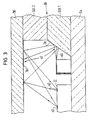
- Bei der Ausführungsform nach Figur 3 besteht der Abstandshalter Ah aus zwei Siliziumschichten Sch1 und Sch2. Die untere Siliziumschicht Sch1 weist eine als Umlenkelement Ue dienende schräge Seitenfläche auf, die durch anisotropes Ätzen hergestellt werden kann.
- Das vom optischen Sender oS, beispielsweise einer Laserdiode, in Richtung des Umlenkelements Ue ausgesandte Licht wird von diesem Umlenkelement Ue zu einer Lichtverteilungseinrichtung Hol umgelenkt, die an der Unterseite des Deckkörpers DK angebracht oder ausgebildet ist und die das zugeleitete Licht auf optische Detektoren oD verteilt, die auf einem Halbleiterchip mit integriertem Schaltkreis IC, beispielsweise in Form von Fotodetektoren, integriert sind. Die Lichtverteilungseinrichtung Hol kann beispielsweise ein Hologramm sein.
- Die Ausführungsform nach Figur 3 hat den Vorteil, daß sie mit den Ausführungsformen nach den Figuren 1 und 2 kompatibel ist.
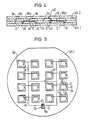
- Die Figuren 4 und 5 zeigen eine Ausführungsform, bei welcher sowohl die optische Verbindung nach den Figuren 1 und 2 als auch die optische Verbindung nach der Figur 3 auf dem gleichen Substrat Su realisiert ist. Das Substrat Su besteht aus einem Siliziumwafer, auf dem eine erste Schicht Sch1 des Abstandshalters Ah fixiert ist, in der rechteckige Bereiche Be ausgespart sind. In jedem rechteckigen Bereich Be ist ein Halbleiterchip mit integriertem Schaltkreis IC und ein optischer Sender oS angeordnet. Auf dieser Schicht Sch1 ist auch eine Streifenwellenleiterstruktur Wst ausgebildet, deren Wellenleiter das von einem optischen Sender oS eines Taktgenerators TG ausgesandte Licht optischen Detektoren oD der verschiedenen integrierten Schaltkreise IC zuleitet.
- In der Figur 5 ist eine Draufsicht auf die Schicht Sch1 mit der Wellenleiterstruktur Wst gezeigt. Die Seitenflächen der ausgesparten Bereiche Be der ersten Schicht Sch1 sind schräg, so daß sie Umlenkelemente Ue bilden können.
- Auf der Wellenleiterstruktur Wst ist eine zweite Schicht Sch2 des Abstandshalters Ah aufgebracht, die ausgesparte Bereiche Be aufweist, die sich mit den ausgesparten Bereichen Be der ersten Schicht Sch1 decken. Auf der zweiten Schicht Sch2 ist der Deckkörper DK aufgebracht. In jedem ausgesparten Bereich Be des Abstandshalters Ah ist auf der Unterseite des Deckkörpers DK ein Lichtverteilungselement Hol angebracht, so daß in jedem Bereich eine optische Verbindung gemäß Figur 3 realisiert ist.
- Die ausgesparten Bereiche Be lassen sich mit hoher Genauigkeit durch Ätzen oder anisotropes Ätzen von Siliziumwafern herstellen. Da für alle Schichten das gleiche Material verwendet ist, treten keine thermischen Spannungen auf.
- Die Fixierung des Substrats Su, des Abstandshalters Ah und des Deckkörpers DK relativ zueinander kann beispielsweise durch Aneinanderkleben oder durch Verschrauben erfolgen.
Claims (22)
wobei der oder die integrierten Schaltkreise (IC), optischen Sender (oS) und optischen Detektoren (oD) in Form von Bausteinen auf einem Substrat (Su) fixiert sind,
wobei auf diesem Substrat (Su) ein Abstandshalter (Ah) aufgebracht ist,
wobei der Abstandshalter (Ah) von einem Deckkörper (DK) abgedeckt ist, und
wobei an dem Abstandshalter (Ah) oder/und dem Deckkörper (DK) eine optische Einrichtung (oE) zum Zuleiten des von einem optischen Sender (oS) ausgesandten Lichts zu einem oder mehreren optischen Detektoren (oD) angebracht ist.
Applications Claiming Priority (2)
| Application Number | Priority Date | Filing Date | Title |
|---|---|---|---|
| DE3811028 | 1988-03-31 | ||
| DE3811028 | 1988-03-31 |
Publications (2)
| Publication Number | Publication Date |
|---|---|
| EP0335104A2 true EP0335104A2 (de) | 1989-10-04 |
| EP0335104A3 EP0335104A3 (de) | 1991-11-06 |
Family
ID=6351182
Family Applications (1)
| Application Number | Title | Priority Date | Filing Date |
|---|---|---|---|
| EP19890103004 Withdrawn EP0335104A3 (de) | 1988-03-31 | 1989-02-21 | Vorrichtung zum optischen Verbinden eines oder mehrerer optischer Sender mit einem oder mehreren optischen Detektoren eines oder mehrerer integrierter Schaltkreise |
Country Status (3)
| Country | Link |
|---|---|
| US (1) | US4871224A (de) |
| EP (1) | EP0335104A3 (de) |
| JP (1) | JPH0210876A (de) |
Cited By (2)
| Publication number | Priority date | Publication date | Assignee | Title |
|---|---|---|---|---|
| EP0508613A1 (de) * | 1991-04-08 | 1992-10-14 | Mitsubishi Denki Kabushiki Kaisha | Multichip-System und Verfahren zur Versorgung von Taktsignalen dafür |
| CN110727046A (zh) * | 2018-07-16 | 2020-01-24 | 上海新微技术研发中心有限公司 | 三维集成光互连芯片中光耦合端面的制造方法 |
Families Citing this family (68)
| Publication number | Priority date | Publication date | Assignee | Title |
|---|---|---|---|---|
| DE3834335A1 (de) * | 1988-10-08 | 1990-04-12 | Telefunken Systemtechnik | Halbleiterschaltung |
| GB8902745D0 (en) * | 1989-02-08 | 1989-03-30 | British Telecomm | Optical interconnection network |
| DE3910710A1 (de) * | 1989-04-03 | 1990-10-04 | Standard Elektrik Lorenz Ag | Optisch-elektrische mehrfachverbindung |
| JPH0642527B2 (ja) * | 1989-10-10 | 1994-06-01 | 日本電気株式会社 | 光導波路を用いた情報処理装置 |
| EP0445488B1 (de) * | 1990-03-08 | 1994-06-01 | International Business Machines Corporation | Halbleiterlaseranordnung |
| US5163113A (en) * | 1990-07-19 | 1992-11-10 | Gte Laboratories Incorporated | Laser-to-fiber coupling apparatus |
| US5243671A (en) * | 1990-07-19 | 1993-09-07 | Gte Laboratories Incorporated | Laser-to-fiber coupling apparatus |
| GB9024713D0 (en) * | 1990-11-14 | 1991-01-02 | Plessey Telecomm | Optical backplane interconnecting circuit boards |
| US5121457A (en) * | 1991-05-21 | 1992-06-09 | Gte Laboratories Incorporated | Method for coupling laser array to optical fiber array |
| US5239189A (en) * | 1991-06-07 | 1993-08-24 | Eastman Kodak Company | Integrated light emitting and light detecting device |
| EP0522417A1 (de) * | 1991-07-09 | 1993-01-13 | Sumitomo Electric Industries, Limited | Licht-Empfangseinrichtung mit Glasfaser-Anschluss |
| US5200631A (en) * | 1991-08-06 | 1993-04-06 | International Business Machines Corporation | High speed optical interconnect |
| US5237434A (en) * | 1991-11-05 | 1993-08-17 | Mcnc | Microelectronic module having optical and electrical interconnects |
| US5268973A (en) * | 1992-01-21 | 1993-12-07 | The University Of Texas System | Wafer-scale optical bus |
| US5401983A (en) * | 1992-04-08 | 1995-03-28 | Georgia Tech Research Corporation | Processes for lift-off of thin film materials or devices for fabricating three dimensional integrated circuits, optical detectors, and micromechanical devices |
| EP0600267B1 (de) * | 1992-12-03 | 1998-01-28 | Siemens Aktiengesellschaft | Bidirektionaler optischer Sende- und Empfangsmodul |
| JPH07131063A (ja) * | 1993-11-01 | 1995-05-19 | Nec Corp | マルチチップモジュール |
| US5416861A (en) * | 1994-04-29 | 1995-05-16 | University Of Cincinnati | Optical synchronous clock distribution network and high-speed signal distribution network |
| US5479540A (en) * | 1994-06-30 | 1995-12-26 | The Whitaker Corporation | Passively aligned bi-directional optoelectronic transceiver module assembly |
| US5500910A (en) * | 1994-06-30 | 1996-03-19 | The Whitaker Corporation | Passively aligned holographic WDM |
| US5886971A (en) * | 1996-09-27 | 1999-03-23 | Digital Optics Corporation | Optical head structures including support substrates adjacent transparent substrates and related methods |
| US5771218A (en) * | 1996-09-27 | 1998-06-23 | Digital Optics Corporation | Passively aligned integrated optical head including light source, detector, and optical element and methods of forming same |
| US5761350A (en) * | 1997-01-22 | 1998-06-02 | Koh; Seungug | Method and apparatus for providing a seamless electrical/optical multi-layer micro-opto-electro-mechanical system assembly |
| US6049639A (en) * | 1997-12-19 | 2000-04-11 | Intel Corporation | Method and apparatus providing optical input/output through the back side of an integrated circuit die |
| US6393169B1 (en) | 1997-12-19 | 2002-05-21 | Intel Corporation | Method and apparatus for providing optical interconnection |
| US6330376B1 (en) | 1997-12-19 | 2001-12-11 | Intel Corporation | Higher order rejection method and apparatus for optical modulator |
| US5978526A (en) * | 1997-12-19 | 1999-11-02 | Motorola, Inc. | Method, multi-channel optical interconnect device, and a multi-channel optically interconnected electronic device for minimizing cross-talk between a plurality of optical signals |
| US6374003B1 (en) | 1997-12-19 | 2002-04-16 | Intel Corporation | Method and apparatus for optically modulating light through the back side of an integrated circuit die using a plurality of optical beams |
| US6075908A (en) * | 1997-12-19 | 2000-06-13 | Intel Corporation | Method and apparatus for optically modulating light through the back side of an integrated circuit die |
| US6052498A (en) * | 1997-12-19 | 2000-04-18 | Intel Corporation | Method and apparatus providing an optical input/output bus through the back side of an integrated circuit die |
| JPH11311721A (ja) * | 1998-02-27 | 1999-11-09 | Oki Electric Ind Co Ltd | 光結合モジュールおよびその製造方法 |
| US6611635B1 (en) | 1998-10-09 | 2003-08-26 | Fujitsu Limited | Opto-electronic substrates with electrical and optical interconnections and methods for making |
| US6690845B1 (en) | 1998-10-09 | 2004-02-10 | Fujitsu Limited | Three-dimensional opto-electronic modules with electrical and optical interconnections and methods for making |
| US6343171B1 (en) | 1998-10-09 | 2002-01-29 | Fujitsu Limited | Systems based on opto-electronic substrates with electrical and optical interconnections and methods for making |
| US6706546B2 (en) | 1998-10-09 | 2004-03-16 | Fujitsu Limited | Optical reflective structures and method for making |
| US6785447B2 (en) | 1998-10-09 | 2004-08-31 | Fujitsu Limited | Single and multilayer waveguides and fabrication process |
| US6684007B2 (en) | 1998-10-09 | 2004-01-27 | Fujitsu Limited | Optical coupling structures and the fabrication processes |
| US6845184B1 (en) | 1998-10-09 | 2005-01-18 | Fujitsu Limited | Multi-layer opto-electronic substrates with electrical and optical interconnections and methods for making |
| US6587605B2 (en) | 1999-01-06 | 2003-07-01 | Intel Corporation | Method and apparatus for providing optical interconnection |
| US20040041081A1 (en) * | 2002-08-30 | 2004-03-04 | Feldman Michael R. | Integrated optical transceiver and related methods |
| US20070181781A1 (en) * | 2001-03-06 | 2007-08-09 | Digital Optics Corporation | Integrated optical transceiver |
| US6501092B1 (en) | 1999-10-25 | 2002-12-31 | Intel Corporation | Integrated semiconductor superlattice optical modulator |
| US6215577B1 (en) | 1999-10-25 | 2001-04-10 | Intel Corporation | Method and apparatus for optically modulating an optical beam with a multi-pass wave-guided optical modulator |
| US6268953B1 (en) | 1999-12-02 | 2001-07-31 | Intel Corporation | Method and apparatus for optically modulating an optical beam with long interaction length optical modulator |
| US6351326B1 (en) | 1999-12-14 | 2002-02-26 | Intel Corporation | Method and apparatus for optically modulating light utilizing a resonant cavity structure |
| JP2001274528A (ja) | 2000-01-21 | 2001-10-05 | Fujitsu Ltd | 薄膜デバイスの基板間転写方法 |
| US7842914B2 (en) * | 2000-03-06 | 2010-11-30 | Tessera North America, Inc. | Optoelectronic package, camera including the same and related methods |
| JP2003526909A (ja) * | 2000-03-06 | 2003-09-09 | ディジタル・オプティックス・コーポレイション | 集積化された光トランシーバおよび関連方法 |
| US6912330B2 (en) | 2001-05-17 | 2005-06-28 | Sioptical Inc. | Integrated optical/electronic circuits and associated methods of simultaneous generation thereof |
| US6690844B2 (en) | 2001-05-17 | 2004-02-10 | Optronx, Inc. | Optical fiber apparatus and associated method |
| US6646747B2 (en) | 2001-05-17 | 2003-11-11 | Sioptical, Inc. | Interferometer apparatus and associated method |
| US6891685B2 (en) * | 2001-05-17 | 2005-05-10 | Sioptical, Inc. | Anisotropic etching of optical components |
| US6748125B2 (en) | 2001-05-17 | 2004-06-08 | Sioptical, Inc. | Electronic semiconductor control of light in optical waveguide |
| US6625348B2 (en) | 2001-05-17 | 2003-09-23 | Optron X, Inc. | Programmable delay generator apparatus and associated method |
| US6526187B1 (en) | 2001-05-17 | 2003-02-25 | Optronx, Inc. | Polarization control apparatus and associated method |
| US6608945B2 (en) | 2001-05-17 | 2003-08-19 | Optronx, Inc. | Self-aligning modulator method and associated apparatus |
| US6654511B2 (en) | 2001-05-17 | 2003-11-25 | Sioptical, Inc. | Optical modulator apparatus and associated method |
| US6603889B2 (en) | 2001-05-17 | 2003-08-05 | Optronx, Inc. | Optical deflector apparatus and associated method |
| US6493502B1 (en) | 2001-05-17 | 2002-12-10 | Optronx, Inc. | Dynamic gain equalizer method and associated apparatus |
| US6947615B2 (en) | 2001-05-17 | 2005-09-20 | Sioptical, Inc. | Optical lens apparatus and associated method |
| US6529318B1 (en) | 2001-08-30 | 2003-03-04 | Np Photonics, Inc. | Total internal reflection (TIR) coupler and method for side-coupling pump light into a fiber |
| DE60206132T2 (de) * | 2002-01-31 | 2006-06-22 | Stmicroelectronics S.R.L., Agrate Brianza | Verfahren und Einrichtung zur hervorragenden galvanischen Isolierung zwischen zwei Niederspannungsschaltungen in einer intergrierten Opto-Isolator-Einrichtung |
| US7043106B2 (en) * | 2002-07-22 | 2006-05-09 | Applied Materials, Inc. | Optical ready wafers |
| US7110629B2 (en) * | 2002-07-22 | 2006-09-19 | Applied Materials, Inc. | Optical ready substrates |
| US20050016446A1 (en) | 2003-07-23 | 2005-01-27 | Abbott John S. | CaF2 lenses with reduced birefringence |
| AU2013230056A1 (en) * | 2012-03-05 | 2014-09-18 | Nanoprecision Products, Inc. | Coupling device having a structured reflective surface for coupling input/output of an optical fiber |
| US9880366B2 (en) | 2015-10-23 | 2018-01-30 | Nanoprecision Products, Inc. | Hermetic optical subassembly |
| US10705302B2 (en) * | 2018-02-27 | 2020-07-07 | Samsung Electronics Co., Ltd. | Photonic integrated circuit packages |
Citations (3)
| Publication number | Priority date | Publication date | Assignee | Title |
|---|---|---|---|---|
| DE2510562A1 (de) * | 1975-03-11 | 1976-09-23 | Siemens Ag | Optoelektronisches koppelelement |
| EP0152597A2 (de) * | 1984-01-24 | 1985-08-28 | Sony Corporation | Vorrichtung zum Aussenden und Empfangen von Lichtsignalen, insbesondere Infrarotsignalen |
| WO1987004566A1 (en) * | 1986-01-21 | 1987-07-30 | American Telephone & Telegraph Company | Interconnects for wafer-scale-integrated assembly |
Family Cites Families (3)
| Publication number | Priority date | Publication date | Assignee | Title |
|---|---|---|---|---|
| US4136928A (en) * | 1977-05-06 | 1979-01-30 | Bell Telephone Laboratories, Incorporated | Optical integrated circuit including junction laser with oblique mirror |
| US4675518A (en) * | 1982-03-05 | 1987-06-23 | Omron Tateisi Electronics Co. | Optical bistable device |
| US4699449A (en) * | 1985-03-05 | 1987-10-13 | Canadian Patents And Development Limited-Societe Canadienne Des Brevets Et D'exploitation Limitee | Optoelectronic assembly and method of making the same |
-
1989
- 1989-02-21 EP EP19890103004 patent/EP0335104A3/de not_active Withdrawn
- 1989-03-13 US US07/322,410 patent/US4871224A/en not_active Expired - Fee Related
- 1989-03-29 JP JP1080204A patent/JPH0210876A/ja active Pending
Patent Citations (3)
| Publication number | Priority date | Publication date | Assignee | Title |
|---|---|---|---|---|
| DE2510562A1 (de) * | 1975-03-11 | 1976-09-23 | Siemens Ag | Optoelektronisches koppelelement |
| EP0152597A2 (de) * | 1984-01-24 | 1985-08-28 | Sony Corporation | Vorrichtung zum Aussenden und Empfangen von Lichtsignalen, insbesondere Infrarotsignalen |
| WO1987004566A1 (en) * | 1986-01-21 | 1987-07-30 | American Telephone & Telegraph Company | Interconnects for wafer-scale-integrated assembly |
Non-Patent Citations (2)
| Title |
|---|
| IBM TECHNICAL DISCLOSURE BULLETIN. Bd. 26, Nr. 4, September 1983, NEW YORK US Seiten 1793 - 1796; L.BALLIET ET AL: 'Optical Transmission System for interconnecting Electronic Units ' * |
| IEEE SPECTRUM. Bd. 24, Nr. 3, M{rz 1987, NEW YORK US Seiten 30 - 35; L.HUTCHESON ET AL: 'Optical interconnects replace hard-wire ' * |
Cited By (4)
| Publication number | Priority date | Publication date | Assignee | Title |
|---|---|---|---|---|
| EP0508613A1 (de) * | 1991-04-08 | 1992-10-14 | Mitsubishi Denki Kabushiki Kaisha | Multichip-System und Verfahren zur Versorgung von Taktsignalen dafür |
| US5250816A (en) * | 1991-04-08 | 1993-10-05 | Mitsubishi Denki Kabushiki Kaisha | Multichip system and method of supplying clock signal therefor |
| CN110727046A (zh) * | 2018-07-16 | 2020-01-24 | 上海新微技术研发中心有限公司 | 三维集成光互连芯片中光耦合端面的制造方法 |
| CN110727046B (zh) * | 2018-07-16 | 2021-07-23 | 上海新微技术研发中心有限公司 | 三维集成光互连芯片中光耦合端面的制造方法 |
Also Published As
| Publication number | Publication date |
|---|---|
| US4871224A (en) | 1989-10-03 |
| EP0335104A3 (de) | 1991-11-06 |
| JPH0210876A (ja) | 1990-01-16 |
Similar Documents
| Publication | Publication Date | Title |
|---|---|---|
| EP0335104A2 (de) | Vorrichtung zum optischen Verbinden eines oder mehrerer optischer Sender mit einem oder mehreren optischen Detektoren eines oder mehrerer integrierter Schaltkreise | |
| EP0366974B1 (de) | Halbleiterschaltung | |
| EP1174745B1 (de) | Optoelektronisches oberflächenmontierbares Modul | |
| EP0731509B1 (de) | Optoelektronischer Wandler und Herstellverfahren | |
| DE3390103C2 (de) | ||
| EP0217063B1 (de) | Optische Anordnung | |
| DE60303140T2 (de) | Optische verbindungsanordnung | |
| DE2754923A1 (de) | Selbstausrichtende optische traegeranordnung fuer optische bauelemente | |
| DE19830360A1 (de) | Opto-elektronischer Modul | |
| DE60215019T2 (de) | Trennung von integrierten optischen modulen und strukturen | |
| DE19727483A1 (de) | Röntgenstrahl-CT-Festkörperdetektor | |
| DE69833611T2 (de) | Ein Mikro-Photonikmodul mit einer Trennwand | |
| DE68929527T2 (de) | Optische Übertragungsvorrichtung | |
| EP1168022A2 (de) | Optomodul mit durchkontaktiertem Trägersubstrat | |
| DE69727343T2 (de) | Optoelektronisches Modul | |
| DE4106721A1 (de) | Anordnung zur ankopplung von lichtwellenleiterenden an empfangselemente | |
| DE102019210750B4 (de) | Verfahren zur herstellung einer anordnung mit einem substrat und zwei bauelementen mit lichtwellenleitern | |
| DE3307669C2 (de) | ||
| DE3939723C1 (en) | Optical or opto-electronic coupling - uses spherical lens received in frusto-pyramidal recess of one part and groove of other part | |
| DE102004038530B3 (de) | Verfahren und Vorrichtung zur Herstellung einer optischen Verbindung zwischen einem optoelektronischen Bauelement und einem Lichtwellenleiter | |
| DE3737251C2 (de) | Halbleiter-Trägerelement für ein elektro-optisches Modul | |
| DE69819502T2 (de) | Verbessertes mikro-photonisches modul auf einem einzelsubstrat | |
| EP1477833B1 (de) | Optoelektronische Sende- und/oder Empfangsanordnung | |
| DE4445997C2 (de) | Anordnung zur Ankopplung einer Lichtleitfaser an ein optisches Bauelement | |
| DE102018214803B4 (de) | Vorrichtung zum Einkoppeln elektromagnetischer Wellen in einen Chip |
Legal Events
| Date | Code | Title | Description |
|---|---|---|---|
| PUAI | Public reference made under article 153(3) epc to a published international application that has entered the european phase |
Free format text: ORIGINAL CODE: 0009012 |
|
| AK | Designated contracting states |
Kind code of ref document: A2 Designated state(s): DE FR GB |
|
| 17P | Request for examination filed |
Effective date: 19901205 |
|
| PUAL | Search report despatched |
Free format text: ORIGINAL CODE: 0009013 |
|
| AK | Designated contracting states |
Kind code of ref document: A3 Designated state(s): DE FR GB |
|
| 17Q | First examination report despatched |
Effective date: 19940510 |
|
| STAA | Information on the status of an ep patent application or granted ep patent |
Free format text: STATUS: THE APPLICATION IS DEEMED TO BE WITHDRAWN |
|
| 18D | Application deemed to be withdrawn |
Effective date: 19950505 |