EP0336514B1 - Method of providing a semiconductor body on a support - Google Patents
Method of providing a semiconductor body on a support Download PDFInfo
- Publication number
- EP0336514B1 EP0336514B1 EP89200843A EP89200843A EP0336514B1 EP 0336514 B1 EP0336514 B1 EP 0336514B1 EP 89200843 A EP89200843 A EP 89200843A EP 89200843 A EP89200843 A EP 89200843A EP 0336514 B1 EP0336514 B1 EP 0336514B1
- Authority
- EP
- European Patent Office
- Prior art keywords
- support
- semiconductor body
- aluminium
- layer
- providing
- Prior art date
- Legal status (The legal status is an assumption and is not a legal conclusion. Google has not performed a legal analysis and makes no representation as to the accuracy of the status listed.)
- Expired - Lifetime
Links
Images
Classifications
-
- H—ELECTRICITY
- H01—ELECTRIC ELEMENTS
- H01L—SEMICONDUCTOR DEVICES NOT COVERED BY CLASS H10
- H01L24/00—Arrangements for connecting or disconnecting semiconductor or solid-state bodies; Methods or apparatus related thereto
- H01L24/80—Methods for connecting semiconductor or other solid state bodies using means for bonding being attached to, or being formed on, the surface to be connected
-
- H—ELECTRICITY
- H01—ELECTRIC ELEMENTS
- H01L—SEMICONDUCTOR DEVICES NOT COVERED BY CLASS H10
- H01L2924/00—Indexing scheme for arrangements or methods for connecting or disconnecting semiconductor or solid-state bodies as covered by H01L24/00
- H01L2924/01—Chemical elements
- H01L2924/01013—Aluminum [Al]
-
- Y—GENERAL TAGGING OF NEW TECHNOLOGICAL DEVELOPMENTS; GENERAL TAGGING OF CROSS-SECTIONAL TECHNOLOGIES SPANNING OVER SEVERAL SECTIONS OF THE IPC; TECHNICAL SUBJECTS COVERED BY FORMER USPC CROSS-REFERENCE ART COLLECTIONS [XRACs] AND DIGESTS
- Y10—TECHNICAL SUBJECTS COVERED BY FORMER USPC
- Y10T—TECHNICAL SUBJECTS COVERED BY FORMER US CLASSIFICATION
- Y10T29/00—Metal working
- Y10T29/49—Method of mechanical manufacture
- Y10T29/49002—Electrical device making
- Y10T29/49117—Conductor or circuit manufacturing
- Y10T29/49124—On flat or curved insulated base, e.g., printed circuit, etc.
- Y10T29/4913—Assembling to base an electrical component, e.g., capacitor, etc.
- Y10T29/49144—Assembling to base an electrical component, e.g., capacitor, etc. by metal fusion
Definitions
- the invention relates to a method of providing a semiconductor body on a support with the interposition of a metal layer of aluminium, in which the adherence is effected in that the semiconductor body and the support are pressed against each other during the supply of heat at the area of the metal layer.
- an aluminium layer is provided on the support, mostly by a galvanic process or the like.
- a continuous smooth aluminium layer is then obtained.
- this layer is provided with notches or the like, however, so that a favourable influence is exerted on the deformability of the aluminium layer when establishing the thermocompression bond between the semiconductor body and the support. If, for example, a semiconductor body must be provided on a support, as is in the case inter alia when providing pn emitters in electron tubes, an additional processing step is required for thus roughening the smooth aluminium layer.
- the invention has for its object to provide a method of the kind mentioned above, in which the disadvantage indicated above can be avoided.
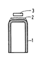
- the sole Figure shows diagrammatically a support 1, for example a cathode support.
- a metal layer 2 consisting of aluminium is applied to this support 1 by means of flame spraying.
- the outer appearance of this layer at its exposed surface automatically becomes rough.
- the unevennesses are shown in the Figure on an exaggerated scale for the sake of clarity.
- this semiconductor body 3 can now be pressed in known manner against the aluminium layer 2 whilst supplying heat to this aluminium layer so that a so-called thermo-compression bond is then established. Due to the rough surface of the aluminium layer 2, this layer is sufficiently deformed so that a good adherence between the semiconductor body and the support is obtained without it being necessary for the aluminium layer to be subjected to an additional processing step beforehand after it has been applied to the support.
Description
- The invention relates to a method of providing a semiconductor body on a support with the interposition of a metal layer of aluminium, in which the adherence is effected in that the semiconductor body and the support are pressed against each other during the supply of heat at the area of the metal layer.
- In such a method, an aluminium layer is provided on the support, mostly by a galvanic process or the like. A continuous smooth aluminium layer is then obtained. In order to promote the adherence between the semiconductor body and the support by means of the aluminium layer, this layer is provided with notches or the like, however, so that a favourable influence is exerted on the deformability of the aluminium layer when establishing the thermocompression bond between the semiconductor body and the support. If, for example, a semiconductor body must be provided on a support, as is in the case inter alia when providing pn emitters in electron tubes, an additional processing step is required for thus roughening the smooth aluminium layer.
- The invention has for its object to provide a method of the kind mentioned above, in which the disadvantage indicated above can be avoided.
- According to the invention, this can be achieved in that the metal layer of aluminium is applied to the support by flame spraying.
- When the aluminium layer is applied by means of flame spraying, a layer having an irregular surface will automatically be formed, as a result of which it is no longer necessary to roughen this surface by etching or notching or the like before the smiconductor body is provided.
- The invention will now be described more fully with reference to the accompanying Figures, which shows diagrammatically a support with a provided aluminium layer and a semiconductor to be provided thereon.
- The sole Figure shows diagrammatically a support 1, for example a cathode support. A metal layer 2 consisting of aluminium is applied to this support 1 by means of flame spraying. When such an aluminium layer 2 is applied by flame spraying, the outer appearance of this layer at its exposed surface automatically becomes rough. The unevennesses are shown in the Figure on an exaggerated scale for the sake of clarity.
- In order to secure a
semiconductor body 3 on the support 1, thissemiconductor body 3 can now be pressed in known manner against the aluminium layer 2 whilst supplying heat to this aluminium layer so that a so-called thermo-compression bond is then established. Due to the rough surface of the aluminium layer 2, this layer is sufficiently deformed so that a good adherence between the semiconductor body and the support is obtained without it being necessary for the aluminium layer to be subjected to an additional processing step beforehand after it has been applied to the support.
Claims (1)
- A method of providing a semiconductor body on a support with the interposition of a metal layer of aluminium, in which the adherence is effected in that the semiconductor body and the support are pressed against each other during the supply of heat at the area of the metal layer, characterized in that the metal layer of aluminium is applied to the support by flame spraying and in that the surface of the semiconductor body on which the support is pressed has no metal layer upon it.
Applications Claiming Priority (2)
| Application Number | Priority Date | Filing Date | Title |
|---|---|---|---|
| NL8800902A NL8800902A (en) | 1988-04-08 | 1988-04-08 | METHOD FOR APPLYING A SEMICONDUCTOR BODY TO A CARRIER. |
| NL8800902 | 1988-04-08 |
Publications (2)
| Publication Number | Publication Date |
|---|---|
| EP0336514A1 EP0336514A1 (en) | 1989-10-11 |
| EP0336514B1 true EP0336514B1 (en) | 1996-07-03 |
Family
ID=19852090
Family Applications (1)
| Application Number | Title | Priority Date | Filing Date |
|---|---|---|---|
| EP89200843A Expired - Lifetime EP0336514B1 (en) | 1988-04-08 | 1989-04-03 | Method of providing a semiconductor body on a support |
Country Status (5)
| Country | Link |
|---|---|
| US (1) | US4961528A (en) |
| EP (1) | EP0336514B1 (en) |
| JP (1) | JP2697890B2 (en) |
| DE (1) | DE68926754T2 (en) |
| NL (1) | NL8800902A (en) |
Families Citing this family (4)
| Publication number | Priority date | Publication date | Assignee | Title |
|---|---|---|---|---|
| US5526977A (en) * | 1994-12-15 | 1996-06-18 | Hayes Wheels International, Inc. | Method for fabricating a bimetal vehicle wheel |
| US5816478A (en) * | 1995-06-05 | 1998-10-06 | Motorola, Inc. | Fluxless flip-chip bond and a method for making |
| US6090643A (en) * | 1998-08-17 | 2000-07-18 | Teccor Electronics, L.P. | Semiconductor chip-substrate attachment structure |
| US6279811B1 (en) * | 2000-05-12 | 2001-08-28 | Mcgraw-Edison Company | Solder application technique |
Family Cites Families (14)
| Publication number | Priority date | Publication date | Assignee | Title |
|---|---|---|---|---|
| CH527487A (en) * | 1971-07-29 | 1972-08-31 | Alusuisse | Method for manufacturing a busbar |
| GB1426874A (en) * | 1972-05-03 | 1976-03-03 | Mullard Ltd | Method of sealing electrical component envelopes |
| IT1111635B (en) * | 1977-10-25 | 1986-01-13 | Bfg Glassgroup | UNITS CONTAINING GLASS ELEMENTS |
| SU703871A2 (en) * | 1977-10-28 | 1979-12-17 | Предприятие П/Я Х-5737 | Method of joining different materials |
| JPS55132048A (en) * | 1979-04-03 | 1980-10-14 | Toshiba Corp | Semiconductor device |
| SU854627A1 (en) * | 1979-09-11 | 1981-08-15 | Предприятие П/Я М-5409 | Method of soldering graphite to aluminium |
| GB2067117B (en) * | 1980-01-02 | 1983-07-06 | Secr Defence | Bonding semi-conductor bodies to aluminium thick-film circuits |
| DE3071367D1 (en) * | 1980-09-29 | 1986-03-06 | Toshiba Kk | A semiconductor device with a semiconductor element soldered on a metal substrate |
| US4448853A (en) * | 1981-04-15 | 1984-05-15 | Bbc Brown, Boveri & Company, Limited | Layered active brazing material and method for producing it |
| JPS5994569A (en) * | 1982-11-24 | 1984-05-31 | Toshiba Corp | Diffusion joining method |
| US4729504A (en) * | 1985-06-01 | 1988-03-08 | Mizuo Edamura | Method of bonding ceramics and metal, or bonding similar ceramics among themselves; or bonding dissimilar ceramics |
| US4817853A (en) * | 1986-11-26 | 1989-04-04 | Sundstrand Corporation | Composite, method of forming a composite, and article of manufacture |
| US4757934A (en) * | 1987-02-06 | 1988-07-19 | Motorola, Inc. | Low stress heat sinking for semiconductors |
| US4905886A (en) * | 1988-07-20 | 1990-03-06 | Grumman Aerospace Corporation | Method for diffusion bonding of metals and alloys using thermal spray deposition |
-
1988
- 1988-04-08 NL NL8800902A patent/NL8800902A/en not_active Application Discontinuation
-
1989
- 1989-03-21 US US07/326,583 patent/US4961528A/en not_active Expired - Fee Related
- 1989-04-03 EP EP89200843A patent/EP0336514B1/en not_active Expired - Lifetime
- 1989-04-03 DE DE68926754T patent/DE68926754T2/en not_active Expired - Fee Related
- 1989-04-05 JP JP1084912A patent/JP2697890B2/en not_active Expired - Lifetime
Non-Patent Citations (8)
| Title |
|---|
| "Ullmans Encyklopädie der Technischen Chemie, Weilheim 1978, page 168; * |
| McGraw Hill: "Encyclopaedia of Science and Technologie" 1982, Vol.4, page 808; * |
| McGraw-Hill Encyclopedia of Science and Technology 1982, vol. 4, page 808 * |
| McGraw-Hill Encyclopedia of Science and Technology 1982, vol. 8, page 398 * |
| McGraw-Hill: "Encyclopädie of Science and Technologie" 1982, Vol. 8, page 398. * |
| Ullmanns Encyclopädie der technischen Chemie, vol. 12, Verlag Chemie, Weinheim, DE, 1978, page 168 * |
| Winnacker-Küchler: "Chemische Technologie", vol. 4: "Metalle"; Carl Hanser Verlag, München, DE, 1986, pages 684 to 686 * |
| Winnaker-Küchler: "Chemische Technologie", Bd.4, Carl Hanser Verlag, München1986, pages 684 to 686; * |
Also Published As
| Publication number | Publication date |
|---|---|
| DE68926754D1 (en) | 1996-08-08 |
| DE68926754T2 (en) | 1997-01-23 |
| US4961528A (en) | 1990-10-09 |
| EP0336514A1 (en) | 1989-10-11 |
| JPH0212805A (en) | 1990-01-17 |
| NL8800902A (en) | 1989-11-01 |
| JP2697890B2 (en) | 1998-01-14 |
Similar Documents
| Publication | Publication Date | Title |
|---|---|---|
| US4393576A (en) | Method of producing electrical contacts on a silicon solar cell | |
| US5767568A (en) | Semiconductor device | |
| EP0738014A3 (en) | Manufacturing method of semiconductor device having capacitor | |
| TW358992B (en) | Semiconductor device and method of fabricating the same | |
| WO2001016402A8 (en) | Electrolytic copper foil with carrier foil and method for manufacturing the same and copper-clad laminate using the electrolytic copper foil with carrier foil | |
| EP0229850A4 (en) | Connection terminals between substrates and method of producing the same. | |
| US3593412A (en) | Bonding system for semiconductor device | |
| TW340243B (en) | Manufacturing method of semiconductor elements | |
| EP0336514B1 (en) | Method of providing a semiconductor body on a support | |
| EP0928022A3 (en) | Resin package fabrication process | |
| EP0895447A3 (en) | A circuit board, a method for manufacturing same, and a method of electroless plating | |
| TW345742B (en) | Method for producing integrated circuit capacitor | |
| WO1992000399A3 (en) | Method for forming a surface coating | |
| EP0337540B1 (en) | Combination of a support and a semiconductor body and method of manufacturing such a combination | |
| EP0884112A3 (en) | Resin-composite aluminum profiles, heat insulating aluminum profiles, and method and apparatus for production thereof | |
| CA2027067A1 (en) | Method for forming a continuous oxide superconductor layer having different thickness portions for superconductor device | |
| EP0128102A3 (en) | Impregnation of aluminum interconnects with copper | |
| MY120359A (en) | Method for manufacturing electronic parts | |
| US6358382B1 (en) | Retaining ring and target and method for producing same | |
| EP1043111A3 (en) | Method of manufacturing beryllium-copper alloy hot isostatic press (Hip) bonded body and hip-bonded body | |
| TW337610B (en) | Structure with reduced stress between a spin-on-glass layer and a metal layer and process for producing the same | |
| SU1109293A1 (en) | Process for manufacturing multilayer panels by diffusion welding | |
| TW324835B (en) | Method for mountong semiconductor | |
| TW353814B (en) | Metallic wiring substrate and producing method thereof | |
| HK1017387A1 (en) | Process for manufacturing inductive counting systems |
Legal Events
| Date | Code | Title | Description |
|---|---|---|---|
| PUAI | Public reference made under article 153(3) epc to a published international application that has entered the european phase |
Free format text: ORIGINAL CODE: 0009012 |
|
| AK | Designated contracting states |
Kind code of ref document: A1 Designated state(s): DE FR GB |
|
| 17P | Request for examination filed |
Effective date: 19900406 |
|
| 17Q | First examination report despatched |
Effective date: 19920331 |
|
| GRAH | Despatch of communication of intention to grant a patent |
Free format text: ORIGINAL CODE: EPIDOS IGRA |
|
| GRAA | (expected) grant |
Free format text: ORIGINAL CODE: 0009210 |
|
| AK | Designated contracting states |
Kind code of ref document: B1 Designated state(s): DE FR GB |
|
| REF | Corresponds to: |
Ref document number: 68926754 Country of ref document: DE Date of ref document: 19960808 |
|
| ET | Fr: translation filed | ||
| PGFP | Annual fee paid to national office [announced via postgrant information from national office to epo] |
Ref country code: GB Payment date: 19970401 Year of fee payment: 9 |
|
| PGFP | Annual fee paid to national office [announced via postgrant information from national office to epo] |
Ref country code: FR Payment date: 19970422 Year of fee payment: 9 |
|
| PLBE | No opposition filed within time limit |
Free format text: ORIGINAL CODE: 0009261 |
|
| STAA | Information on the status of an ep patent application or granted ep patent |
Free format text: STATUS: NO OPPOSITION FILED WITHIN TIME LIMIT |
|
| PGFP | Annual fee paid to national office [announced via postgrant information from national office to epo] |
Ref country code: DE Payment date: 19970624 Year of fee payment: 9 |
|
| 26N | No opposition filed | ||
| PG25 | Lapsed in a contracting state [announced via postgrant information from national office to epo] |
Ref country code: GB Free format text: LAPSE BECAUSE OF NON-PAYMENT OF DUE FEES Effective date: 19980403 |
|
| PG25 | Lapsed in a contracting state [announced via postgrant information from national office to epo] |
Ref country code: FR Free format text: THE PATENT HAS BEEN ANNULLED BY A DECISION OF A NATIONAL AUTHORITY Effective date: 19980430 |
|
| GBPC | Gb: european patent ceased through non-payment of renewal fee |
Effective date: 19980403 |
|
| PG25 | Lapsed in a contracting state [announced via postgrant information from national office to epo] |
Ref country code: DE Free format text: LAPSE BECAUSE OF NON-PAYMENT OF DUE FEES Effective date: 19990202 |
|
| REG | Reference to a national code |
Ref country code: FR Ref legal event code: ST |
|
| APAH | Appeal reference modified |
Free format text: ORIGINAL CODE: EPIDOSCREFNO |