EP0338742A2 - Direct digital synthesizer with selectably randomized accumulator - Google Patents
Direct digital synthesizer with selectably randomized accumulator Download PDFInfo
- Publication number
- EP0338742A2 EP0338742A2 EP89303760A EP89303760A EP0338742A2 EP 0338742 A2 EP0338742 A2 EP 0338742A2 EP 89303760 A EP89303760 A EP 89303760A EP 89303760 A EP89303760 A EP 89303760A EP 0338742 A2 EP0338742 A2 EP 0338742A2
- Authority
- EP
- European Patent Office
- Prior art keywords
- accumulator
- output
- circuitry
- adder
- frequency
- Prior art date
- Legal status (The legal status is an assumption and is not a legal conclusion. Google has not performed a legal analysis and makes no representation as to the accuracy of the status listed.)
- Granted
Links
Images
Classifications
-
- H—ELECTRICITY
- H03—ELECTRONIC CIRCUITRY
- H03C—MODULATION
- H03C3/00—Angle modulation
-
- G—PHYSICS
- G06—COMPUTING; CALCULATING OR COUNTING
- G06F—ELECTRIC DIGITAL DATA PROCESSING
- G06F1/00—Details not covered by groups G06F3/00 - G06F13/00 and G06F21/00
- G06F1/02—Digital function generators
- G06F1/03—Digital function generators working, at least partly, by table look-up
- G06F1/035—Reduction of table size
- G06F1/0353—Reduction of table size by using symmetrical properties of the function, e.g. using most significant bits for quadrant control
-
- G—PHYSICS
- G06—COMPUTING; CALCULATING OR COUNTING
- G06F—ELECTRIC DIGITAL DATA PROCESSING
- G06F2101/00—Indexing scheme relating to the type of digital function generated
- G06F2101/04—Trigonometric functions
-
- G—PHYSICS
- G06—COMPUTING; CALCULATING OR COUNTING
- G06F—ELECTRIC DIGITAL DATA PROCESSING
- G06F2211/00—Indexing scheme relating to details of data-processing equipment not covered by groups G06F3/00 - G06F13/00
- G06F2211/902—Spectral purity improvement for digital function generators by adding a dither signal, e.g. noise
Definitions
- the invention relates generally to digital frequency synthesizer apparatus, and more particularly to such apparatus employing an accumulator for synthesizing a selected frequency of a number of preselected frequencies in conjunction with a randomizer which adds random or pseudorandom values to a selectable few of the least significant bits of the accumulator.
- Direct Digital Frequency Synthesis is a digital technique of frequency synthesis that is often used in phase and frequency modulation and frequency hopping schemes in spread spectrum communications. This technique is advantageous because of the speed at which frequency can be changed, the small frequency step size possible, and the digital control of phase or frequency available.
- An apparatus employing this technique is referred to as a Direct Digital Synthesizer or "DDS.”
- the output frequency of a DDS is determined by an input digital frequency control word.
- This frequency control word can be generated by a digital processor.
- Many modulation schemes can be implemented, for example, FSK, FM, PM, DPSK, etc.
- the output frequency can be frequency modulated according to the information digitized by the processor (FSK modulation).
- FSK modulation the window of modulated frequencies can hop, thereby moving the window of modulated frequencies in a coded scheme to avoid jamming or decoding by unauthorized transceivers. It is the agility and the frequency resolution of the DDS that makes it superior to other synthesizers in such an application and gives an unauthorized transceiver less time to lock on the correct frequency and then jam or decode it. Naturally, the authorized receiver must hop to the correct frequency to receive the modulated information.
- the receiver's digital processor generates the correct digital control word for the receiver's DDS and subsequent down-conversion, demodulation, and decoding.
- the heart of the Direct Digital Synthesizer is the accumulator.
- the accumulator is a digital integrator consisting of a latch and full adder with the output sum and the input digital control word as inputs to the adder.
- the frequency word determines the step size by which the accumulated sum is incremented. Each step represents a step or increment in phase; thus, larger frequency words result in larger steps in phase.
- the rate of overflow of the accumulator determines the output frequency.
- the output frequency is a fraction of the clock frequency; thus its spurious performance has similarities to a fractional divider. However, some frequencies are not submultiples of the clock frequency, and the accumulator overflow occurs with varying remainders left in the accumulator.
- the residue left in the accumulator varies the output periods such that a sequence of different output periods result.
- the average of this sequence of periods is the desired period and, thus, determines the output frequency.
- spurious line frequencies or "spurs" unique to each output frequency are created. Such spurs represent departure of the output waveform from a precisely periodic signal.
- the spurious levels will be significant.
- the conventional method used to suppress these spurious frequencies utilizes a sine approximation technique. This technique essentially consists of the accumulator, a sine look-up table in Read Only Memory (ROM), a digital analog converter (DAC), and an output filter. The instantaneous error from an ideal sinusoidal frequency of constant period is reduced; therefore, the spurious levels are suppressed.
- Wheatley U.S. Patent No. 4,410,954 discloses an apparatus for feeding a value corresponding to a selected phase increment at a clock rate to an adder, which is in mutual cooperation with an accumulator. The resultant periodic overflow of the accumulator corresponds to the selected frequency of interest. Additional cooperating apparatus is provided for generating a random sequence of values. The difference between any one of these values and the selected phase increment is less than the selected phase increment. Jitter logic is responsive to the overflow output of the accumulator to add or subtract a sequential one of the random values to or from the phase increment value as an input to the accumulator for at least one clock interval occurring within the duration between successive overflows of the accumulator.
- the Wheatley dithered DDS has a binary output; therefore, it has the advantage that no ROM or DAC is needed.
- the Wheatley method randomly varies or dithers the accumulator at each overflow or alternate overflows such that the edges or just one edge of the binary output are dithered.
- the Wheatley circuit thus reduces spurs by summing a random value with a uniform distribution up to the selected phase increment or "input vector.”
- the Wheatley operation introduces flat phase noise, although, in many applications, the introduced flat phase noise is within the phase noise performance margin and hence does not limit system performance, whereas the spurious performance attributable to spurs in the absence of spur reduction would limit system performance.
- a second disadvantage of the Wheatley circuit is the lack of flexibility in selecting between the amount of spur reduction and phase noise. Since the dither is uniform up to the input vector, a trade-off between spur reduction and phase noise is established. With Wheatley's circuit, selectability between these two performance criteria can be achieved only through selection of the clock rate, a relatively inflexible approach.
- DDS direct digital synthesizer
- an accumulator applicable in a DDS is employed in conjunction with a randomizer that adds random or pseudorandom values to a selectable few of the least significant bits of the accumulator to introduce flat or nearly flat frequency deviation density in the vicinity of significant spurs for spurious frequency suppression, instead of dithering enough bits of the accumulator to introduce flat phase noise as in prior art.
- the frequency deviation density at the spur's offset in frequency from the carrier effectively spreads the energy of the spur; therefore, by this technique all in-band spurs are equally reduced.
- the invention particularly departs significantly from the approach taught by Wheatley.
- the random value is uniformly distributed over a range which is not up to and just less than the input vector as taught by Wheatley, but is rather much less than the input vector for a given set of system specifications.
- the random value added to the accumulator is not necessarily subtracted out and can be allowed to circulate in the accumulator. Permitting the random value to circulate in the accumulator results in a known offset in output frequency. This offset can be subtracted from the input digital frequency control word (input vector) in applications where it proves objectionable.
- An additional advantage is that, if the bits dithered are below the lowest input vector for a given output bandwidth, the dithering no longer needs to be sensitive to the input vector. This significantly reduces the complexity of the hardware since the comparator and memory (stack) in the prior art Wheatley circuit are no longer required.
- the accumulator can be sectioned into additional pipelined stages, and the dither can be implemented without decreasing throughput. In fact, the accumulator can be lengthened while maintaining the same number of LSB's dithered. As a result, the spurs are spread into as low a level as before, but the phase noise introduced by dithering is reduced.
- the levels of all in-band sampling spurs are reduced, including the spurs close-in to the fundamental, which the prior art is ineffective in reducing.
- the dither introduces a frequency deviation of the signal which is less than the frequency offset of the closest spur to the fundamental. Consequently, the frequency deviation density at the offset frequencies of the spurs is constant, and all in-band spurs are reduced by the same amount including the close-in spurs.
- the number of bits dithered is selectable and the accumulator can be any length, a wide range of spur levels and phase noise trade-offs are possible.
- the number of bits dithered may be selected by hardwiring or by processor or other digital control.
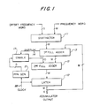
- FIG. 1 A dithered accumulator circuit according to the preferred embodiment is shown in FIG. 1.
- This circuit employs a subtractor 11 which receives an M-bit frequency word or "input vector" on a first input and subtracts from it a D-bit offset frequency word supplied on a second input.
- the output of the subtractor 11 is supplied as one input to a first full adder 13, which receives a second input from the output of a latch 19.
- the first full adder 13 outputs an M-bit word to one input of a second full adder 15 and an overflow bit to an enable gate 17.
- the second full adder 15 receives a second D-bit input from the enable gate 17 and outputs an M-bit output to the latch 19.
- the accumulator output comprises K bits where K ⁇ M.
- a pseudorandom number (PRN) generator 21 provides a D-bit pseudorandom number to the enable gate 17.
- the pseudorandom number generator 21 and the latch 19 receive a clock input on a clock line 22.
- the accumulator may be viewed as an integrator which integrates phase increments, ⁇ 0 ⁇ , at its input, represented by the frequency control word, to yield an output K representing phase 0 ⁇ .
- the accumulator consists of an adder and a latch, analogous to the first full adder 13 and the latch 19.
- the embodiment of the invention includes a second full adder 15, enable gate 17 and pseudorandom number generator 21.
- the second full adder 15 adds the pseudorandom number from the PRN generator 21 to the output of the first full adder 13.
- the pseudorandom number is added only when an overflow occurs from the first full adder 13. Such an overflow is signalled over a line 14 from the first full adder to the enable gate 17, which then gates the pseudorandom number to the second full adder 15.
- the pseudorandom number added to the output of the first full adder 13 is selected to satisfy the following equation: Where f m ′ is the frequency offset in the spur closest to the fundamental, f CLK is the clock frequency on line 22, which updates the latch 19 and clocks the number generator 21, D is the number of bits in the PRN generator 21 and in the offset frequency word, and M is the number of bits in the input vector. To satisfy this equation, the number of bits “D” in general must be very small compared to "M.” If "D" becomes too large, the right-hand side of the equation becomes much greater than the offset in the frequency spectrum of the first spur, f m ′ and effectiveness in reducing close-in spurs is decreased.
- the second full adder 15 When the pseudorandom number is added in by the second full adder 15, a slight frequency offset occurs. Depending on system specifications and the amount of dither added in, it may be unnecessary to compensate for this offset. In such case, the subtractor 11 is not required. For example, if only one or two bits are dithered, i.e., D «M, it will cause a very small offset in the output frequency. It may be noted that the second full adder 15 can be placed elsewhere in the circuit, for example in the place of the subtractor 11.
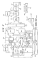
- FIG. 2 illustrates the incorporation of the preferred embodiment into a pipelined DDS circuit.
- the circuitry within the dashed line 66 comprises the dithering circuitry 66 according to the invention, while the remaining circuitry comprises a typical sine look-up DDS.
- This embodiment employs an accumulator sectioned into stages in order to maintain throughput of the pipelined system.
- the dithering circuitry 66 receives a frequency word which is shifted serially into a shift register 53 clocked by a clock on a line 68.
- a twenty-bit frequency word is used as an example.
- the twenty-bit frequency word is input in parallel to a latch 51.
- the latch 51 is activated by a control line when a strobe (LOAD), e.g., from a digital processor, is supplied to a clocked timing circuit 57, which synchronizes the edge of the load strobe with the DDS system clock (CLK).
- LOAD strobe
- CLK DDS system clock
- the four least significant bits of the output of the latch 51 are transmitted to one input of a four bit adder 49, while the other sixteen bits contained in the latch 51 are transmitted to one input of a sixteen bit adder 50.
- Six carry generate and propagate outputs of the sixteen bit adder 50 are outputted to a look ahead carry generator 37, which supplies an overflow bit on a line 38 to one input of a dither generator 43.
- the other input of the dither generator 43 is connected to receive the output 42 of the four bit adder 49 and has a four bit output 46 connected to a latch 41.
- the four bit output of the latch 41 is connected as the input to the four bit adder 49.
- the four bit adder 49, sixteen bit adder 50 and look ahead carry generator 37 comprise the first full adder 13 of FIG. 1. Accordingly, the carry-out line 44 of the four bit adder 49 is connected to the carry-in input of the sixteen bit adder 50 and to the carry generator 37.
- the dither generator 43 includes the pseudorandom number generator 21, the enable gate 17 and the second full adder 15 illustrated in FIG. 1. Thus, the first full adder 13 of FIG.
- the sixteen bit adder 50 outputs to a sixteen bit latch 31. This latch 31 and the latch 41 perform the function of the latch 19 in FIG. 1.
- the circuitry for configuring the addresses includes a buffer 33, exclusive-or gates 35 for performing the one's complement, and a latch 39.
- the twelve most significant bits of the latch 31 are supplied to the first input of the one's complement circuit 35.
- the output of the latch 31 is fed back to the second input of the sixteen bit adder 50.
- the two least significant bits are supplied as an input to the buffer 33, which provides a large fanout to thirteen bits.
- the twelve significant bits of the output of the buffer 33 form the second input into the comparator 35.
- the one's complement circuit 35 comprises an exclusive-or (EX-OR) of respective pairs of the twelve incoming bits on first and second input lines from the latch 31 and the buffer 33.
- the upper four bits of the output of the one's complement circuit 35 are supplied to the first four bit positions of a twenty bit latch 39 and to the second four bit positions of the latch 39.
- the second four bits output by the one's complement circuit 35 are supplied to the next four bit positions of the latch 39 and to the next four bit positions of the latch 39.
- the last four bits of the twenty bit latch 39 are filled by the last four bits output by the comparator circuit 35.
- the twenty output bits of the latch 39 are connected to address the respective ROM's 45, 47.
- the two read-only memory circuits 45, 47 supply a fifteen bit output to the latch 55.
- the latch 55 further receives the most significant bit from the latch 39 and transfers that most significant bit, which is the sign bit, to a buffer 59.
- the outputs of the table look-up operation respectively, eleven bits from ROM 45 and four bits from ROM 47, are added by an eleven-bit adder 60 which outputs nine bits to a one's complement circuit 61.
- the one's complement circuit 61 receives a nine bit input from the buffer 59, and outputs nine bits to a latch 63.
- Latch 63 also receives the sign bit from the buffer 59.
- the latch 63 supplies a ten bit digital output to a digital to analog converter 67.
- the one's complement circuit 61 supplies the appropriate sign to the output since only one quadrant of the sinewave is stored in the read-only memory circuits 45, 47.
- a buffer tree timing generator 65 is also supplied to provide appropriate clock signals to the circuitry.
- the desired output of the DDS is a sinusoidal signal; therefore, the closer the output approximates the sinewave the better the output spectral purity will be.
- the digital approach of FIG. 2 is to use a sine look-up table in ROM which is addressed by the output of the accumulator 66. The ROM output is then input to a DAC for an approximation to the desired output sinewave. The accuracy of the approximated output will depend on the phase information contained in the accumulator, truncation in the sine algorithm and DAC, and other DAC errors.
- the sine approximation technique used in the embodiment of FIG. 2 is unmodified from the DDS LSI design of Sunderland et al.
- Sunderland's DDS sine algorithm utilizes a well-known technique of ROM reduction by storing only one quadrant of the symmetrical sinewave in memory.
- his DDS design utilizes a unique trigonometric reduction to substantially reduce the memory requirements further.
- the two terms on the Right Hand Side of equation (3) represent the separation of the ROM into the two parts shown in FIG. 2: a coarse ROM 45 (of size 256x11) and a fine ROM 47 (of size 256x4).
- the two terms are added together by the eleven bit adder 60 and combined with the sign bit for a twelve bit offset binary output to the DAC 67, which is truncated to ten bits in the embodiment shown.
- the one's complement circuit 35 preceding the ROM's 45, 47 decodes the quadrant, while the one's complement circuit 61 following the eleven bit adder 60 decodes the sign.
- phase information propagates through the DDS from the accumulator latch 31, to the ROM latch 39, to the ROM latch 55, to the DAC latch 63 with each step, from latch to latch, representing a pipelined stage.
- Each stage must settle within a clock period, and the throughput is determined by the clock period, the number of pipelined stages, and the settling time of the DAC 67.
- the twenty bit accumulator 66 of FIG. 2 is sectioned into a sixteen bit high accumulator 50 and four bit low accumulator 49.
- the carry of the low accumulator 49 into the LSB of the high accumulator 50 is truncated in the sine approximation algorithm and DAC 67: the twelve bits retained in the sine algorithm represents the truncation of the least significant four bits of the sixteen bit high accumulator 50.
- a DAC 67 with ten bits of resolution represents additional truncation. Therefore, the carry from the low accumulator 49 can lag behind the high accumulator 50 by one clock cycle without affecting the significance of the bits in the sine algorithm. Similarly, additional accumulator sections can be added to the accumulator.
- the low accumulator 49 is parallel to the high accumulator 50 and requires only a four bit adder, the low accumulator 49 is an advantageous place to inject dither without decreasing the DDS throughput.
- a pseudorandom value can be added to the low accumulator 49 to inject dither at each overflow of the high accumulator 50. But the previous random number which Wheatley subtracted from the accumulator may require a borrow from the high accumulator. If the previous random number is not subtracted out, the average of the random value will offset the output frequency just as though this average value had been added to the frequency control word. Since the pseudorandom number generator has a known average value, it can simply be subtracted from the frequency control word.
- a twenty bit subtractor is required. To avoid the twenty bit subtractor, the carry which is added to the high accumulator 50 can be effectively subtracted out later by removing a "1" from the LSB of the high accumulator register when such a condition occurs. Care must be taken not to subtract this bit out too soon, or the random phase values may not accumulate to the extent necessary to generate the carry into the significant bits which address the sine ROM's 45, 47.
- the random value is added to the accumulator sum before the accumulator latch 41, but it can be added anywhere in the accumulator loop or at the input vector. It is assumed that the overflow from the low accumulator 49 would not affect more than the least significant bit of the high accumulator 50. If the input vector to the low accumulator 49 is not zero, the possibility of carries into the two least significant bits of the high accumulator 50 could be required in one clock period. One way of avoiding this problem is to extend the accumulator, such that the lowest section of the accumulator 49, which is dithered, is lower in significance than the LSB of the input vector. The condition for the greatest spurs occurs when only a few of the MSBs are high and the LSBs of the accumulator are zero.
- the DDS implementation In order to determine the requirements for the random number generator 21, the DDS implementation must be considered. At exactly half the clock frequency, the alias will coincide with the output frequency. The alias occurs at the frequency determined by subtracting the output frequency from the clock frequency. The output frequency must be less than the alias by a margin necessary for the transition region of the output alias filter (a low pass filter to filter out the alias). Therefore, the random number generator 21 must have a propagation delay which is at most slightly less than twice the clock period at the highest possible DDS output frequency.
- a suitable random number generator is a design by Rader et al. disclosed in the article "A Fast Method of Generating Digital Random Numbers," The Bell System Technical Journal, November 1970.
- This design has a delay equal to the settling time of a flip-flop and the propagation delay of an exclusive-or gate.
- the DAC 67 is the final stage in the disclosed DDS. Following the DAC 67 is a filter for smoothing the output sinewave and reducing the alias amplitude (not shown in FIG. 2). The performance of the DAC 67 is of concern since the spurious performance of the DDS can be affected.
- the circuitry disclosed in FIG. 2 is all digital and can be implemented in Very High Speed Integrated circuit (VHSIC) technology with clock rates in the gigahertz.
- VHSIC Very High Speed Integrated circuit
- the DAC 67 must settle to within a specified accuracy to the desired level within one clock period.
- the spectral performance of the DDS is degraded by DAC errors.
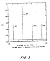
- FIG. 3 shows spurs 101, 103, 105, typically present about the fundamental 107 in the output of a DDS with an undithered accumulator.
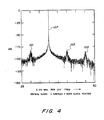
- the preferred embodiment functions to suppress the amplitude of such spurs 101, 103, 105 as shown in FIG. 4.
- Suppression of the close-in spurs 101, 103 is a particular advantage of the invention over the prior art.
- the spectrum of FIG. 4 exhibits decreasing phase noise with frequency offset from the output frequency and therefore has a substantially flat frequency deviation density and reduces all spurs including those close-in.
Abstract
Description
- The invention relates generally to digital frequency synthesizer apparatus, and more particularly to such apparatus employing an accumulator for synthesizing a selected frequency of a number of preselected frequencies in conjunction with a randomizer which adds random or pseudorandom values to a selectable few of the least significant bits of the accumulator.
- In the design of radio communications systems, a continuing goal has been the design of a simple, low-cost frequency synthesizer that can provide a large library of discrete frequencies over a very wide frequency spectrum. Design efforts toward this goal have introduced an associated spectrum of spurious outputs, the minimization of which has not been entirely successful or satisfactory.
- Prior art approaches have typically been too complex for commercial feasibility. Most such prior-art solutions employ digital logic and have required the use of hybrid devices such as digital-to-analog (D/A) converters, as well as table look-up devices such as sine/cosine Read Only Memories (ROM's). A primary purpose of these additional elements has been to reduce the poor output spectral quality. Such associated poor output spectral quality is mainly evidenced by the presence of a large number of unwanted or spurious line spectral components referred to commonly as "spurs."
- Direct Digital Frequency Synthesis is a digital technique of frequency synthesis that is often used in phase and frequency modulation and frequency hopping schemes in spread spectrum communications. This technique is advantageous because of the speed at which frequency can be changed, the small frequency step size possible, and the digital control of phase or frequency available. An apparatus employing this technique is referred to as a Direct Digital Synthesizer or "DDS."
- The output frequency of a DDS is determined by an input digital frequency control word. This frequency control word can be generated by a digital processor. Many modulation schemes can be implemented, for example, FSK, FM, PM, DPSK, etc. Thus, for example, the output frequency can be frequency modulated according to the information digitized by the processor (FSK modulation). In addition to the FSK modulation, the window of modulated frequencies can hop, thereby moving the window of modulated frequencies in a coded scheme to avoid jamming or decoding by unauthorized transceivers. It is the agility and the frequency resolution of the DDS that makes it superior to other synthesizers in such an application and gives an unauthorized transceiver less time to lock on the correct frequency and then jam or decode it. Naturally, the authorized receiver must hop to the correct frequency to receive the modulated information. The receiver's digital processor generates the correct digital control word for the receiver's DDS and subsequent down-conversion, demodulation, and decoding.
- The heart of the Direct Digital Synthesizer is the accumulator. The accumulator is a digital integrator consisting of a latch and full adder with the output sum and the input digital control word as inputs to the adder. The frequency word determines the step size by which the accumulated sum is incremented. Each step represents a step or increment in phase; thus, larger frequency words result in larger steps in phase. In addition, the rate of overflow of the accumulator determines the output frequency. The output frequency is a fraction of the clock frequency; thus its spurious performance has similarities to a fractional divider. However, some frequencies are not submultiples of the clock frequency, and the accumulator overflow occurs with varying remainders left in the accumulator. The residue left in the accumulator varies the output periods such that a sequence of different output periods result. The average of this sequence of periods is the desired period and, thus, determines the output frequency. However, since this sequence of periods is also different from an ideal repetition of the exact period, spurious line frequencies or "spurs" unique to each output frequency are created. Such spurs represent departure of the output waveform from a precisely periodic signal.
- If the overflow of the accumulator is used to generate a binary output, the spurious levels will be significant. The conventional method used to suppress these spurious frequencies utilizes a sine approximation technique. This technique essentially consists of the accumulator, a sine look-up table in Read Only Memory (ROM), a digital analog converter (DAC), and an output filter. The instantaneous error from an ideal sinusoidal frequency of constant period is reduced; therefore, the spurious levels are suppressed.
- An alternative to such solutions is disclosed in Wheatley U.S. Patent No. 4,410,954. That patent discloses an apparatus for feeding a value corresponding to a selected phase increment at a clock rate to an adder, which is in mutual cooperation with an accumulator. The resultant periodic overflow of the accumulator corresponds to the selected frequency of interest. Additional cooperating apparatus is provided for generating a random sequence of values. The difference between any one of these values and the selected phase increment is less than the selected phase increment. Jitter logic is responsive to the overflow output of the accumulator to add or subtract a sequential one of the random values to or from the phase increment value as an input to the accumulator for at least one clock interval occurring within the duration between successive overflows of the accumulator. The Wheatley dithered DDS has a binary output; therefore, it has the advantage that no ROM or DAC is needed.
- The Wheatley method randomly varies or dithers the accumulator at each overflow or alternate overflows such that the edges or just one edge of the binary output are dithered. The Wheatley circuit thus reduces spurs by summing a random value with a uniform distribution up to the selected phase increment or "input vector." However, the Wheatley operation introduces flat phase noise, although, in many applications, the introduced flat phase noise is within the phase noise performance margin and hence does not limit system performance, whereas the spurious performance attributable to spurs in the absence of spur reduction would limit system performance.
- One disadvantage of the Wheatley circuit is that the frequency deviation density decreases with decreasing frequency offset. Hence, the deviation density is inadequate to reduce close-in spurs, i.e., those spurs near the desired frequency output.
- A second disadvantage of the Wheatley circuit is the lack of flexibility in selecting between the amount of spur reduction and phase noise. Since the dither is uniform up to the input vector, a trade-off between spur reduction and phase noise is established. With Wheatley's circuit, selectability between these two performance criteria can be achieved only through selection of the clock rate, a relatively inflexible approach.
- It is therefore an object of the invention to improve direct digital synthesizer (DDS) circuitry.
- It is another object of the invention to improve DDS circuits employing an accumulator as a frequency generator.
- It is yet another object of the invention to provide a DDS employing an accumulator frequency generator in which close-in spurs are effectively reduced.
- According to the invention, an accumulator applicable in a DDS is employed in conjunction with a randomizer that adds random or pseudorandom values to a selectable few of the least significant bits of the accumulator to introduce flat or nearly flat frequency deviation density in the vicinity of significant spurs for spurious frequency suppression, instead of dithering enough bits of the accumulator to introduce flat phase noise as in prior art. The frequency deviation density at the spur's offset in frequency from the carrier effectively spreads the energy of the spur; therefore, by this technique all in-band spurs are equally reduced.
- The invention particularly departs significantly from the approach taught by Wheatley. The random value is uniformly distributed over a range which is not up to and just less than the input vector as taught by Wheatley, but is rather much less than the input vector for a given set of system specifications. In addition, the random value added to the accumulator is not necessarily subtracted out and can be allowed to circulate in the accumulator. Permitting the random value to circulate in the accumulator results in a known offset in output frequency. This offset can be subtracted from the input digital frequency control word (input vector) in applications where it proves objectionable. An additional advantage is that, if the bits dithered are below the lowest input vector for a given output bandwidth, the dithering no longer needs to be sensitive to the input vector. This significantly reduces the complexity of the hardware since the comparator and memory (stack) in the prior art Wheatley circuit are no longer required. Additionally, in a sine DDS design, if the significance of the low bits are truncated in the sine approximation algorithm, the accumulator can be sectioned into additional pipelined stages, and the dither can be implemented without decreasing throughput. In fact, the accumulator can be lengthened while maintaining the same number of LSB's dithered. As a result, the spurs are spread into as low a level as before, but the phase noise introduced by dithering is reduced.
- For a direct digital synthesizer employing the invention, the levels of all in-band sampling spurs are reduced, including the spurs close-in to the fundamental, which the prior art is ineffective in reducing. The dither introduces a frequency deviation of the signal which is less than the frequency offset of the closest spur to the fundamental. Consequently, the frequency deviation density at the offset frequencies of the spurs is constant, and all in-band spurs are reduced by the same amount including the close-in spurs.
- In addition, since the number of bits dithered is selectable and the accumulator can be any length, a wide range of spur levels and phase noise trade-offs are possible. The number of bits dithered may be selected by hardwiring or by processor or other digital control.
- The just-summarized invention will now be described in conjunction with the drawings of which:
- FIG. 1 is a block diagram of accumulator circuitry according to the preferred embodiment of the invention;
- FIG. 2 is a circuit block diagram of a DDS circuit employing the preferred embodiment of the invention;
- FIG. 3 illustrates spurs present about the fundamental in the output of an undithered accumulator; and
- FIG. 4 illustrates suppression of spurs according to the preferred embodiment.
- A dithered accumulator circuit according to the preferred embodiment is shown in FIG. 1. This circuit employs a
subtractor 11 which receives an M-bit frequency word or "input vector" on a first input and subtracts from it a D-bit offset frequency word supplied on a second input. The output of thesubtractor 11 is supplied as one input to a firstfull adder 13, which receives a second input from the output of alatch 19. The firstfull adder 13 outputs an M-bit word to one input of a secondfull adder 15 and an overflow bit to an enable gate 17. The secondfull adder 15 receives a second D-bit input from the enable gate 17 and outputs an M-bit output to thelatch 19. The accumulator output comprises K bits where K ≦ M. A pseudorandom number (PRN)generator 21 provides a D-bit pseudorandom number to the enable gate 17. Thepseudorandom number generator 21 and thelatch 19 receive a clock input on aclock line 22. The accumulator may be viewed as an integrator which integrates phase increments, Δ0̸, at its input, represented by the frequency control word, to yield an output K representing phase 0̸. - In typical prior art DDS circuits, the accumulator consists of an adder and a latch, analogous to the first
full adder 13 and thelatch 19. The embodiment of the invention includes a secondfull adder 15, enable gate 17 andpseudorandom number generator 21. As will be appreciated, the secondfull adder 15 adds the pseudorandom number from thePRN generator 21 to the output of the firstfull adder 13. The pseudorandom number is added only when an overflow occurs from the firstfull adder 13. Such an overflow is signalled over aline 14 from the first full adder to the enable gate 17, which then gates the pseudorandom number to the secondfull adder 15. The pseudorandom number added to the output of the firstfull adder 13 is selected to satisfy the following equation:
line 22, which updates thelatch 19 and clocks thenumber generator 21, D is the number of bits in thePRN generator 21 and in the offset frequency word, and M is the number of bits in the input vector. To satisfy this equation, the number of bits "D" in general must be very small compared to "M." If "D" becomes too large, the right-hand side of the equation becomes much greater than the offset in the frequency spectrum of the first spur, fm′ and effectiveness in reducing close-in spurs is decreased. - When the pseudorandom number is added in by the second
full adder 15, a slight frequency offset occurs. Depending on system specifications and the amount of dither added in, it may be unnecessary to compensate for this offset. In such case, thesubtractor 11 is not required. For example, if only one or two bits are dithered, i.e., D«M, it will cause a very small offset in the output frequency. It may be noted that the secondfull adder 15 can be placed elsewhere in the circuit, for example in the place of thesubtractor 11. - Selection of the number of bits "D" to be very small satisfies the relationship of equation (1) and therefore results in the desired substantially flat frequency deviation density for suppression of close-in spurs. It is also possible to achieve such flat frequency deviation density by arranging the circuitry to decode certain conditions where worst case spurs occur and respond to such conditions to randomize the accumulator.
- FIG. 2 illustrates the incorporation of the preferred embodiment into a pipelined DDS circuit. The circuitry within the dashed
line 66 comprises the ditheringcircuitry 66 according to the invention, while the remaining circuitry comprises a typical sine look-up DDS. This embodiment employs an accumulator sectioned into stages in order to maintain throughput of the pipelined system. - The dithering
circuitry 66 receives a frequency word which is shifted serially into a shift register 53 clocked by a clock on a line 68. In the illustration shown, a twenty-bit frequency word is used as an example. The twenty-bit frequency word is input in parallel to alatch 51. Thelatch 51 is activated by a control line when a strobe (LOAD), e.g., from a digital processor, is supplied to a clockedtiming circuit 57, which synchronizes the edge of the load strobe with the DDS system clock (CLK). The four least significant bits of the output of thelatch 51 are transmitted to one input of a fourbit adder 49, while the other sixteen bits contained in thelatch 51 are transmitted to one input of a sixteenbit adder 50. Six carry generate and propagate outputs of the sixteenbit adder 50 are outputted to a look ahead carrygenerator 37, which supplies an overflow bit on aline 38 to one input of adither generator 43. The other input of thedither generator 43 is connected to receive theoutput 42 of the fourbit adder 49 and has a fourbit output 46 connected to alatch 41. The four bit output of thelatch 41 is connected as the input to the fourbit adder 49. - In the embodiment of the
dither circuit 66 shown in FIG. 2, the fourbit adder 49, sixteenbit adder 50 and look ahead carrygenerator 37 comprise the firstfull adder 13 of FIG. 1. Accordingly, the carry-outline 44 of the fourbit adder 49 is connected to the carry-in input of the sixteenbit adder 50 and to thecarry generator 37. Thedither generator 43 includes thepseudorandom number generator 21, the enable gate 17 and the secondfull adder 15 illustrated in FIG. 1. Thus, the firstfull adder 13 of FIG. 1 is sectioned into twoparts dither generator 43 is latched into thelatch 41 and then added into the fourbit adder 49 for accumulation of the lower section of the accumulator represented by the part of the M bits fromlatch 19 which lead back to the input of the firstfull adder 13 of FIG. 1. The sixteenbit adder 50 outputs to a sixteenbit latch 31. Thislatch 31 and thelatch 41 perform the function of thelatch 19 in FIG. 1. - Those skilled in the art will recognize the circuitry of FIG. 2 outside of dashed
line 66 as typical DDS circuitry employing a sine approximation technique and quadrant decoding method to generate addresses for a sine look-up table stored in read only memory (ROM)circuits gates 35 for performing the one's complement, and alatch 39. The twelve most significant bits of thelatch 31 are supplied to the first input of the one'scomplement circuit 35. The output of thelatch 31 is fed back to the second input of the sixteenbit adder 50. The two least significant bits are supplied as an input to the buffer 33, which provides a large fanout to thirteen bits. The twelve significant bits of the output of the buffer 33 form the second input into thecomparator 35. The one'scomplement circuit 35 comprises an exclusive-or (EX-OR) of respective pairs of the twelve incoming bits on first and second input lines from thelatch 31 and the buffer 33. The upper four bits of the output of the one'scomplement circuit 35 are supplied to the first four bit positions of a twentybit latch 39 and to the second four bit positions of thelatch 39. The second four bits output by the one'scomplement circuit 35 are supplied to the next four bit positions of thelatch 39 and to the next four bit positions of thelatch 39. The last four bits of the twentybit latch 39 are filled by the last four bits output by thecomparator circuit 35. - According to the quadrant decoding method, the twenty output bits of the
latch 39 are connected to address the respective ROM's 45, 47. The two read-only memory circuits latch 55. Thelatch 55 further receives the most significant bit from thelatch 39 and transfers that most significant bit, which is the sign bit, to abuffer 59. The outputs of the table look-up operation, respectively, eleven bits fromROM 45 and four bits fromROM 47, are added by an eleven-bit adder 60 which outputs nine bits to a one'scomplement circuit 61. The one'scomplement circuit 61 receives a nine bit input from thebuffer 59, and outputs nine bits to alatch 63.Latch 63 also receives the sign bit from thebuffer 59. Thelatch 63 supplies a ten bit digital output to a digital toanalog converter 67. As those skilled in the art will recognize, the one'scomplement circuit 61 supplies the appropriate sign to the output since only one quadrant of the sinewave is stored in the read-only memory circuits tree timing generator 65 is also supplied to provide appropriate clock signals to the circuitry. - The desired output of the DDS is a sinusoidal signal; therefore, the closer the output approximates the sinewave the better the output spectral purity will be. The digital approach of FIG. 2 is to use a sine look-up table in ROM which is addressed by the output of the
accumulator 66. The ROM output is then input to a DAC for an approximation to the desired output sinewave. The accuracy of the approximated output will depend on the phase information contained in the accumulator, truncation in the sine algorithm and DAC, and other DAC errors. - The sine approximation technique used in the embodiment of FIG. 2 is unmodified from the DDS LSI design of Sunderland et al. Sunderland's DDS sine algorithm utilizes a well-known technique of ROM reduction by storing only one quadrant of the symmetrical sinewave in memory. In addition, his DDS design utilizes a unique trigonometric reduction to substantially reduce the memory requirements further. The argument of the sine function is separated into three terms, and the following trigonometric identity is applied:
sin (A + B + C) = sin (A + B) cos C + cos A cos B sin C - sin A sin B sin C (2)
Approximations are made, and the equation becomes
sin (A + B + C) ≅ sin (A + B) + cos A sin C (3)
Compensation is added to the terms B and C to reduce the errors introduced by the approximation. The reader is referred to Sunderland et al., "CMOS/SOS Frequency Synthesizer LSI Circuit for Spread Spectrum Communications," IEEE Journal of Solid-State Circuits, Vol. SC-19, No. 4, August 1984, for further details of this approximation. The two terms on the Right Hand Side of equation (3) represent the separation of the ROM into the two parts shown in FIG. 2: a coarse ROM 45 (of size 256x11) and a fine ROM 47 (of size 256x4). The two terms are added together by the elevenbit adder 60 and combined with the sign bit for a twelve bit offset binary output to theDAC 67, which is truncated to ten bits in the embodiment shown. The one'scomplement circuit 35 preceding the ROM's 45, 47 decodes the quadrant, while the one'scomplement circuit 61 following the elevenbit adder 60 decodes the sign. The phase information propagates through the DDS from theaccumulator latch 31, to theROM latch 39, to theROM latch 55, to theDAC latch 63 with each step, from latch to latch, representing a pipelined stage. Each stage must settle within a clock period, and the throughput is determined by the clock period, the number of pipelined stages, and the settling time of theDAC 67. - The twenty
bit accumulator 66 of FIG. 2 is sectioned into a sixteen bithigh accumulator 50 and four bitlow accumulator 49. The carry of thelow accumulator 49 into the LSB of thehigh accumulator 50 is truncated in the sine approximation algorithm and DAC 67: the twelve bits retained in the sine algorithm represents the truncation of the least significant four bits of the sixteen bithigh accumulator 50. ADAC 67 with ten bits of resolution represents additional truncation. Therefore, the carry from thelow accumulator 49 can lag behind thehigh accumulator 50 by one clock cycle without affecting the significance of the bits in the sine algorithm. Similarly, additional accumulator sections can be added to the accumulator. - Since the
low accumulator 49 is parallel to thehigh accumulator 50 and requires only a four bit adder, thelow accumulator 49 is an advantageous place to inject dither without decreasing the DDS throughput. A pseudorandom value can be added to thelow accumulator 49 to inject dither at each overflow of thehigh accumulator 50. But the previous random number which Wheatley subtracted from the accumulator may require a borrow from the high accumulator. If the previous random number is not subtracted out, the average of the random value will offset the output frequency just as though this average value had been added to the frequency control word. Since the pseudorandom number generator has a known average value, it can simply be subtracted from the frequency control word. If the processor is not capable of this, a twenty bit subtractor is required. To avoid the twenty bit subtractor, the carry which is added to thehigh accumulator 50 can be effectively subtracted out later by removing a "1" from the LSB of the high accumulator register when such a condition occurs. Care must be taken not to subtract this bit out too soon, or the random phase values may not accumulate to the extent necessary to generate the carry into the significant bits which address the sine ROM's 45, 47. - The random value is added to the accumulator sum before the
accumulator latch 41, but it can be added anywhere in the accumulator loop or at the input vector. It is assumed that the overflow from thelow accumulator 49 would not affect more than the least significant bit of thehigh accumulator 50. If the input vector to thelow accumulator 49 is not zero, the possibility of carries into the two least significant bits of thehigh accumulator 50 could be required in one clock period. One way of avoiding this problem is to extend the accumulator, such that the lowest section of theaccumulator 49, which is dithered, is lower in significance than the LSB of the input vector. The condition for the greatest spurs occurs when only a few of the MSBs are high and the LSBs of the accumulator are zero. - In order to determine the requirements for the
random number generator 21, the DDS implementation must be considered. At exactly half the clock frequency, the alias will coincide with the output frequency. The alias occurs at the frequency determined by subtracting the output frequency from the clock frequency. The output frequency must be less than the alias by a margin necessary for the transition region of the output alias filter (a low pass filter to filter out the alias). Therefore, therandom number generator 21 must have a propagation delay which is at most slightly less than twice the clock period at the highest possible DDS output frequency. A suitable random number generator is a design by Rader et al. disclosed in the article "A Fast Method of Generating Digital Random Numbers," The Bell System Technical Journal, November 1970. This design has a delay equal to the settling time of a flip-flop and the propagation delay of an exclusive-or gate. Rader lists the sequence period for register lengths from L=1 to 25. A longer sequence period represents a better pseudorandom number approximation to a true random number. Rader shows a period of 159783 for L=13, which requires a reasonable amount of hardware, and it has a good autocorrelation function of noise generation. The distribution is uniform, and any number of bits required (up to thirteen) for dithering can be selected from it to dither the accumulator of the DDS. - The
DAC 67 is the final stage in the disclosed DDS. Following theDAC 67 is a filter for smoothing the output sinewave and reducing the alias amplitude (not shown in FIG. 2). The performance of theDAC 67 is of concern since the spurious performance of the DDS can be affected. The circuitry disclosed in FIG. 2 is all digital and can be implemented in Very High Speed Integrated circuit (VHSIC) technology with clock rates in the gigahertz. TheDAC 67, however, must settle to within a specified accuracy to the desired level within one clock period. In addition, the spectral performance of the DDS is degraded by DAC errors. - At the state-of-the-art, Hewlett-Packard Laboratories has developed a twelve bit GaAs DAC capable of conversion rates of 1 gigaword/s. The packaging required for linearity performance at full speed requires microwave techniques. Such a design demonstrates the advancements being made in DAC technology and will certainly have application in advanced DDS designs. However, conversion rates of typical off-the-shelf ten bit DACs can range up to 100 megawords/s, which has proved satisfactory in simulations of the circuit of FIG. 2.
- The operation of the preferred embodiment in suppressing spurs may be graphically illustrated using FIGS. 3 and 4. FIG. 3 shows spurs 101, 103, 105, typically present about the fundamental 107 in the output of a DDS with an undithered accumulator. The preferred embodiment functions to suppress the amplitude of
such spurs spurs - The foregoing discussion has illustrated a dithered accumulator circuit and its application to reduce spurs in the output of a DDS circuit. Those skilled in the art will appreciate that many adaptations and variations of the disclosed embodiments may be made without departing from the scope and spirit of the invention. Therefore, it is to be understood that, within the scope of the appended claims, the invention may be practiced other than as specifically described herein.
Claims (9)
said first adder (13) includes an overflow output;
said circuitry further comprises a second adder (15) coupled between and to the first adder (13) and the latch (19); and
said circuitry further comprises enable means for receiving the overflow output of the first adder (13) and for receiving the pseudorandom number and applying said pseudorandom number to the second adder upon receiving the overflow from said first adder (13).
said frequency control value comprises a binary frequency control word;
said second adder (15) adds the pseudorandom number to a selected few of the least significant bits of said binary frequency control word; and
said latch (19) comprises means for storing a binary word and updating said binary word in accordance with a selected clock rate.

the lower order accumulator means (49) receives a selected number of the lower order bits of said frequency control word;
the circuitry further includes dither generator means (43) for dithering a selected few of said low order bits; and
the higher order accumulator means (50) receives a selected number of the higher order bits of said frequency control word and the output of said low order accumulator means (49) for generating the output.
the circuitry further comprises an input latch means (51) for latching said frequency control word and supplying said frequency control word to said lower order accumulator means (49); and
the circuitry further comprises lower order latch means for latching the output of said lower order accumulator means (49) and supplying it to said higher order accumulator means (50).
Applications Claiming Priority (2)
| Application Number | Priority Date | Filing Date | Title |
|---|---|---|---|
| US184642 | 1988-04-22 | ||
| US07/184,642 US4951237A (en) | 1988-04-22 | 1988-04-22 | Direct digital synthesizer with selectably randomized accumulator |
Publications (3)
| Publication Number | Publication Date |
|---|---|
| EP0338742A2 true EP0338742A2 (en) | 1989-10-25 |
| EP0338742A3 EP0338742A3 (en) | 1991-10-30 |
| EP0338742B1 EP0338742B1 (en) | 1995-01-04 |
Family
ID=22677744
Family Applications (1)
| Application Number | Title | Priority Date | Filing Date |
|---|---|---|---|
| EP89303760A Expired - Lifetime EP0338742B1 (en) | 1988-04-22 | 1989-04-17 | Direct digital synthesizer with selectably randomized accumulator |
Country Status (4)
| Country | Link |
|---|---|
| US (1) | US4951237A (en) |
| EP (1) | EP0338742B1 (en) |
| JP (1) | JP2659022B2 (en) |
| IL (1) | IL89846A (en) |
Cited By (10)
| Publication number | Priority date | Publication date | Assignee | Title |
|---|---|---|---|---|
| EP0454917A1 (en) * | 1990-05-02 | 1991-11-06 | Hewlett-Packard Limited | Frequency synthesiser |
| WO1995017039A1 (en) * | 1993-12-14 | 1995-06-22 | Forschungszentrum Jülich GmbH | Narrow band, arbitrary hf modulation and noise generator |
| EP0823700A2 (en) * | 1996-08-06 | 1998-02-11 | Nds Limited | Digital syntesizer |
| WO2000054401A1 (en) * | 1999-03-11 | 2000-09-14 | Siemens Aktiengesellschaft | Method for generating a signal with adjustable frequency using a dither signal generator |
| WO2001018637A1 (en) * | 1999-09-02 | 2001-03-15 | Siemens Aktiengesellschaft | Improvement of the spectral characteristics in direct digital frequencies synthesis |
| WO2004082146A2 (en) * | 2004-02-10 | 2004-09-23 | Raytheon Company | Digital-phase to digital amplitude translator with first bit off priority coded output for input to unit weighed digital to analog converter |
| EP1351397A3 (en) * | 2001-11-27 | 2005-03-02 | Texas Instruments Incorporated | All-digital frequency synthesis with capacitive re-introduction of dithered tuning information |
| WO2005062736A2 (en) * | 2003-12-11 | 2005-07-14 | Advanced Radio Corporation | Wideband dds synthesizer |
| US7302237B2 (en) | 2002-07-23 | 2007-11-27 | Mercury Computer Systems, Inc. | Wideband signal generators, measurement devices, methods of signal generation, and methods of signal analysis |
| US7525351B2 (en) | 2003-10-30 | 2009-04-28 | Marvell International Technology Ltd. | Fixed frequency clock output having a variable high frequency input clock and an unrelated fixed frequency reference signal |
Families Citing this family (27)
| Publication number | Priority date | Publication date | Assignee | Title |
|---|---|---|---|---|
| US5386398A (en) * | 1990-12-28 | 1995-01-31 | Massachusetts Institute Of Technology | Display of partly randomized time |
| JPH05218895A (en) * | 1992-01-31 | 1993-08-27 | Nec Corp | Receiver |
| US5235613A (en) * | 1992-03-02 | 1993-08-10 | The Boeing Company | Frequency hopping method and apparatus |
| US5329260A (en) * | 1992-07-17 | 1994-07-12 | Ii Morrow Inc. | Numerically-controlled modulated oscillator and modulation method |
| US5305362A (en) * | 1992-12-10 | 1994-04-19 | Hewlett-Packard Company | Spur reduction for multiple modulator based synthesis |
| JPH06224879A (en) * | 1993-01-22 | 1994-08-12 | Mitsui Mining & Smelting Co Ltd | Transmitter for spread spectrum communication and lsi for the same |
| JPH0763124B2 (en) * | 1993-02-24 | 1995-07-05 | 日本電気株式会社 | Direct digital frequency synthesizer |
| US5291428A (en) * | 1993-03-02 | 1994-03-01 | Harris Corporation | Apparatus for reducing spurious frequency components in the output signal of a direct digital synthesizer |
| US5598437A (en) * | 1993-07-16 | 1997-01-28 | Litton Systems, Inc. | Multichannel frequency and phase variable radio frequency simulator |
| US5467294A (en) * | 1994-03-09 | 1995-11-14 | Hu; Vince | High speed, low power direct digital synthesizer |
| US5521533A (en) * | 1994-09-16 | 1996-05-28 | Rockwell International | Apparatus and method for spurious signal reduction in direct-digital synthesizers |
| JP3268138B2 (en) * | 1994-09-29 | 2002-03-25 | 三菱電機株式会社 | Communication device, frequency synthesizer and synthesis method |
| US5598440A (en) * | 1994-11-08 | 1997-01-28 | Mpb Technologies Inc. | DDS driven DDS synthesizer for generating sinewave waveforms with reduced spurious signal levels |
| SE506694C2 (en) * | 1994-12-12 | 1998-02-02 | Ericsson Telefon Ab L M | Device and method for reducing undesirable frequency components in digital frequency generation |
| US5602874A (en) * | 1994-12-29 | 1997-02-11 | Motorola, Inc. | Method and apparatus for reducing quantization noise |
| US5841808A (en) * | 1995-03-23 | 1998-11-24 | Mcdonnell Douglas Corporation | Spread spectrum chip rate tracking system |
| US5691931A (en) * | 1995-06-07 | 1997-11-25 | Hitachi America, Ltd. | Low power adder for accumulation |
| US5673212A (en) * | 1995-09-01 | 1997-09-30 | Motorola, Inc. | Method and apparatus for numerically controlled oscillator with partitioned phase accumulator |
| US6748407B1 (en) * | 1999-02-03 | 2004-06-08 | Nec Corporation | Direct digital synthesizer |
| WO2001008311A1 (en) * | 1999-07-21 | 2001-02-01 | Siemens Aktiengesellschaft | Clock signal generator |
| US6353649B1 (en) * | 2000-06-02 | 2002-03-05 | Motorola, Inc. | Time interpolating direct digital synthesizer |
| US7023368B1 (en) * | 2004-08-31 | 2006-04-04 | Euvis, Inc. | Digital-to-analog signal converting apparatus and method to extend usable spectrum over Nyquist frequency |
| EP1882304B1 (en) * | 2005-05-10 | 2018-08-15 | Texas Instruments Incorporated | Fast hopping frequency synthesizer using an all digital phased locked loop (adpll) |
| US7599977B2 (en) * | 2005-08-16 | 2009-10-06 | Reveal Imaging, Llc | Direct digital synthesizer system and related methods |
| US8594251B2 (en) | 2011-06-22 | 2013-11-26 | Broadcom Corporation | Long-term drift mitigation for radio frequency receivers utilizing a free-running crystal |
| US8542784B2 (en) * | 2011-06-22 | 2013-09-24 | Broadcom Corporation | Spur mitigation for radio frequency receivers utilizing a free-running crystal |
| JP2018506101A (en) * | 2014-12-31 | 2018-03-01 | メガチップス テクノロジー アメリカ コーポレーション | Clock generator and processor system |
Citations (4)
| Publication number | Priority date | Publication date | Assignee | Title |
|---|---|---|---|---|
| US4206425A (en) * | 1978-08-29 | 1980-06-03 | Rca Corporation | Digitized frequency synthesizer |
| US4410954A (en) * | 1980-10-08 | 1983-10-18 | Rockwell International Corporation | Digital frequency synthesizer with random jittering for reducing discrete spectral spurs |
| US4652832A (en) * | 1985-07-05 | 1987-03-24 | Motorola, Inc. | Frequency resolution in a digital oscillator |
| SU1584065A1 (en) * | 1988-05-23 | 1990-08-07 | Предприятие П/Я Г-4149 | Digital frequency synthesizer |
Family Cites Families (3)
| Publication number | Priority date | Publication date | Assignee | Title |
|---|---|---|---|---|
| US4752902A (en) * | 1985-07-08 | 1988-06-21 | Sciteq Electronics, Inc. | Digital frequency synthesizer |
| US4815018A (en) * | 1985-12-24 | 1989-03-21 | Hughes Aircraft Company | Spurless fractional divider direct digital frequency synthesizer and method |
| US4809205A (en) * | 1986-11-19 | 1989-02-28 | Rockwell International Corporation | Digital sine conversion circuit for use in direct digital synthesizers |
-
1988
- 1988-04-22 US US07/184,642 patent/US4951237A/en not_active Expired - Lifetime
-
1989
- 1989-04-04 IL IL89846A patent/IL89846A/en not_active IP Right Cessation
- 1989-04-17 EP EP89303760A patent/EP0338742B1/en not_active Expired - Lifetime
- 1989-04-21 JP JP1103307A patent/JP2659022B2/en not_active Expired - Lifetime
Patent Citations (4)
| Publication number | Priority date | Publication date | Assignee | Title |
|---|---|---|---|---|
| US4206425A (en) * | 1978-08-29 | 1980-06-03 | Rca Corporation | Digitized frequency synthesizer |
| US4410954A (en) * | 1980-10-08 | 1983-10-18 | Rockwell International Corporation | Digital frequency synthesizer with random jittering for reducing discrete spectral spurs |
| US4652832A (en) * | 1985-07-05 | 1987-03-24 | Motorola, Inc. | Frequency resolution in a digital oscillator |
| SU1584065A1 (en) * | 1988-05-23 | 1990-08-07 | Предприятие П/Я Г-4149 | Digital frequency synthesizer |
Cited By (14)
| Publication number | Priority date | Publication date | Assignee | Title |
|---|---|---|---|---|
| EP0454917A1 (en) * | 1990-05-02 | 1991-11-06 | Hewlett-Packard Limited | Frequency synthesiser |
| WO1995017039A1 (en) * | 1993-12-14 | 1995-06-22 | Forschungszentrum Jülich GmbH | Narrow band, arbitrary hf modulation and noise generator |
| EP0823700A2 (en) * | 1996-08-06 | 1998-02-11 | Nds Limited | Digital syntesizer |
| EP0823700A3 (en) * | 1996-08-06 | 1998-09-23 | Nds Limited | Digital syntesizer |
| WO2000054401A1 (en) * | 1999-03-11 | 2000-09-14 | Siemens Aktiengesellschaft | Method for generating a signal with adjustable frequency using a dither signal generator |
| WO2001018637A1 (en) * | 1999-09-02 | 2001-03-15 | Siemens Aktiengesellschaft | Improvement of the spectral characteristics in direct digital frequencies synthesis |
| EP1351397A3 (en) * | 2001-11-27 | 2005-03-02 | Texas Instruments Incorporated | All-digital frequency synthesis with capacitive re-introduction of dithered tuning information |
| US7302237B2 (en) | 2002-07-23 | 2007-11-27 | Mercury Computer Systems, Inc. | Wideband signal generators, measurement devices, methods of signal generation, and methods of signal analysis |
| DE102004033105B4 (en) * | 2003-10-30 | 2009-07-16 | Marvell International Technology Ltd. | A fixed frequency clock output having a variable high frequency input clock and a disjointed fixed frequency reference signal |
| US7525351B2 (en) | 2003-10-30 | 2009-04-28 | Marvell International Technology Ltd. | Fixed frequency clock output having a variable high frequency input clock and an unrelated fixed frequency reference signal |
| WO2005062736A2 (en) * | 2003-12-11 | 2005-07-14 | Advanced Radio Corporation | Wideband dds synthesizer |
| WO2005062736A3 (en) * | 2003-12-11 | 2006-09-14 | Advanced Radio Corp | Wideband dds synthesizer |
| WO2004082146A3 (en) * | 2004-02-10 | 2004-11-18 | Raytheon Co | Digital-phase to digital amplitude translator with first bit off priority coded output for input to unit weighed digital to analog converter |
| WO2004082146A2 (en) * | 2004-02-10 | 2004-09-23 | Raytheon Company | Digital-phase to digital amplitude translator with first bit off priority coded output for input to unit weighed digital to analog converter |
Also Published As
| Publication number | Publication date |
|---|---|
| EP0338742B1 (en) | 1995-01-04 |
| US4951237A (en) | 1990-08-21 |
| IL89846A (en) | 1992-07-15 |
| EP0338742A3 (en) | 1991-10-30 |
| JPH0263305A (en) | 1990-03-02 |
| JP2659022B2 (en) | 1997-09-30 |
Similar Documents
| Publication | Publication Date | Title |
|---|---|---|
| EP0338742B1 (en) | Direct digital synthesizer with selectably randomized accumulator | |
| US6717998B2 (en) | Frequency synthesizer apparatus equipped with fraction part control circuit, communication apparatus, frequency modulator apparatus, and frequency modulating method | |
| EP1469373B1 (en) | Direct digital frequency synthesizer for cellular wireless communication systems based on fast frequency-hopped spread spectrum technology | |
| US6707855B2 (en) | Digital delta sigma modulator in a fractional-N frequency synthesizer | |
| US10090845B1 (en) | Fraction-N digital PLL capable of canceling quantization noise from sigma-delta modulator | |
| US5563535A (en) | Direct digital frequency synthesizer using sigma-delta techniques | |
| US7385539B2 (en) | All-digital phase locked loop (ADPLL) system | |
| US5821816A (en) | Integer division variable frequency synthesis apparatus and method | |
| US7324030B2 (en) | Multiple stage delta sigma modulators | |
| US5598440A (en) | DDS driven DDS synthesizer for generating sinewave waveforms with reduced spurious signal levels | |
| JP4275502B2 (en) | Fractional N frequency synthesizer and fractional N frequency synthesizer method | |
| US11804847B2 (en) | Fractional frequency synthesis by sigma-delta modulating frequency of a reference clock | |
| US5986483A (en) | Direct digital frequency systhesizer | |
| US6785345B2 (en) | Frequency dithering for DDS spectral purity | |
| US6756927B2 (en) | Sigma-delta programming device for a PLL frequency synthesizer, configuration using the sigma-delta programming device, PLL frequency device, and method for programming a programmable device | |
| US5424664A (en) | Direct digital synthesizer with adjustable clock frequency | |
| US10560111B2 (en) | Nested cascaded mixed-radix digital delta-sigma modulator | |
| US7385537B2 (en) | Linear feedback shift register first-order noise generator | |
| Vankka | A direct digital synthesizer with a tunable error feedback structure | |
| CA2370254A1 (en) | Improvements relating to frequency synthesisers | |
| EP0452031A2 (en) | Signal generation using digital-to-analogue conversion | |
| US20230327681A1 (en) | Digital delta sigma modulator with inherent spur immunity after nonlinear distortion | |
| US6662002B2 (en) | Frequency conversion circuit and transmitter | |
| Sadatnoori | A Fourth-order MASH DDSM for Accurate Fractional Frequency Synthesizers | |
| WO2003001677A2 (en) | Digital-to-analog converter device and digital-to-analog conversion method |
Legal Events
| Date | Code | Title | Description |
|---|---|---|---|
| PUAI | Public reference made under article 153(3) epc to a published international application that has entered the european phase |
Free format text: ORIGINAL CODE: 0009012 |
|
| AK | Designated contracting states |
Kind code of ref document: A2 Designated state(s): FR GB |
|
| PUAL | Search report despatched |
Free format text: ORIGINAL CODE: 0009013 |
|
| AK | Designated contracting states |
Kind code of ref document: A3 Designated state(s): FR GB |
|
| 17P | Request for examination filed |
Effective date: 19920402 |
|
| 17Q | First examination report despatched |
Effective date: 19930913 |
|
| GRAA | (expected) grant |
Free format text: ORIGINAL CODE: 0009210 |
|
| AK | Designated contracting states |
Kind code of ref document: B1 Designated state(s): FR GB |
|
| ET | Fr: translation filed | ||
| PLBE | No opposition filed within time limit |
Free format text: ORIGINAL CODE: 0009261 |
|
| STAA | Information on the status of an ep patent application or granted ep patent |
Free format text: STATUS: NO OPPOSITION FILED WITHIN TIME LIMIT |
|
| 26N | No opposition filed | ||
| REG | Reference to a national code |
Ref country code: GB Ref legal event code: 732E |
|
| REG | Reference to a national code |
Ref country code: FR Ref legal event code: CD Ref country code: FR Ref legal event code: CA Ref country code: FR Ref legal event code: TP |
|
| REG | Reference to a national code |
Ref country code: GB Ref legal event code: IF02 |
|
| PGFP | Annual fee paid to national office [announced via postgrant information from national office to epo] |
Ref country code: GB Payment date: 20080320 Year of fee payment: 20 |
|
| PGFP | Annual fee paid to national office [announced via postgrant information from national office to epo] |
Ref country code: FR Payment date: 20080313 Year of fee payment: 20 |
|
| REG | Reference to a national code |
Ref country code: GB Ref legal event code: PE20 Expiry date: 20090416 |
|
| PG25 | Lapsed in a contracting state [announced via postgrant information from national office to epo] |
Ref country code: GB Free format text: LAPSE BECAUSE OF EXPIRATION OF PROTECTION Effective date: 20090416 |