EP0338757A2 - A cell stack for variable digit width serial architecture - Google Patents
A cell stack for variable digit width serial architecture Download PDFInfo
- Publication number
- EP0338757A2 EP0338757A2 EP89303799A EP89303799A EP0338757A2 EP 0338757 A2 EP0338757 A2 EP 0338757A2 EP 89303799 A EP89303799 A EP 89303799A EP 89303799 A EP89303799 A EP 89303799A EP 0338757 A2 EP0338757 A2 EP 0338757A2
- Authority
- EP
- European Patent Office
- Prior art keywords
- cell
- cells
- stack
- stacks
- disposed
- Prior art date
- Legal status (The legal status is an assumption and is not a legal conclusion. Google has not performed a legal analysis and makes no representation as to the accuracy of the status listed.)
- Granted
Links
Images


Classifications
-
- G—PHYSICS
- G06—COMPUTING; CALCULATING OR COUNTING
- G06F—ELECTRIC DIGITAL DATA PROCESSING
- G06F30/00—Computer-aided design [CAD]
- G06F30/30—Circuit design
Definitions
- a cell stack for digit serial digital circuit systems comprises a cap cell, a plurality of operation cells capable of carrying out single bit serial operations and a control cell.
- the cap cell, operation cells and the control cell are arranged in a vertical stack in which each cell is of approximately the same width so as to define a width for the overall cell stack.
- the cap cell is configured to provide power from one side of a power supply to the operation cells and to the control cell and to provide a means for supplying power to adjacently disposed cell stacks from one side of a power supply.
- the control cell is configured to provide power from a second side of the power supply to the operation cells and to provide a means for supplying power to adjacently disposed cell stacks.
- An aspect of the present invention seeks to facilitate the design of serial operators for use on integrated circuit devices.
Abstract
Description
- The present invention is generally directed to a cell stack architecture which is particularly useful for constructing variable digit width electronic circuits for digital signal processing. More particularly, the present invention is directed to a cell stack architecture which allows the construction of a number of basic cell stacks from libraries of computational circuit elements so as to permit a number of cell stacks to be easily assembled to carry out digit serial operations for any digit size within reasonable bounds. Cell stack arrays fabricated from the corresponding cell stack library are used to address a wide range of digital signal processing applications.
- A proper understanding of the present invention can only be had through an understanding of bit serial and digit serial digital signal processing (DSP) architecture. In bit serial computation, data streams arrive at various computational elements a single bit at a time rather than all at once as in a fully parallel architecture. Bit serial architectures generate a single bit of output in each fundamental clock cycle. The advantage of bit serial architecture is that it is very simple to implement and to design and consumes very little "chip real estate" in integrated circuit devices. Bit serial architectures have often been perceived as having a disadvantage not only of a long latency time, but also the disadvantage of a low throughput even after the pipeline delay latency period has elapsed.
- The present applicants have discerned that in any given digital signal processing problem, optimal results in terms of throughput and chip real estate actually require an architecture which draws both upon serial and upon parallel computational philosophies. To this end, applicants have proven that, in general, optimal design requires the utilization of digit serial architectural circuit designs. In these designs, bits re grouped together in digits having 2, 3, 4, 5, 6 or more bits and these "parallel" digits are processed in a serial fashion. Thus, in digit serial architecture, a data word is divided into a number of digits of fixed, but initially arbitrary width. Arithmetic data flow within the circuit is over digit-wide signal lines and is propagated with the least significant digit first. Thus, data arrives serially at each operator, one digit at a time. Arithmetic and logic operators perform digit-serial calculations on this data and provide digit-serial output. In order to exploit this architecture fully, it is necessary to accommodate arbitrary digit widths up to some reasonable maximum. say NMAX. Typically, NMAX is 12 or 16 but is not limited thereto. It is noted though that once an optimal digit width is determined for a particular signal processing system which is to be implemented on one or more integrated circuit chips, the digit width is fixed for circuit components appearing on that chip.
- In the design of circuit chips to carry out digital serial processing applications, it has become very desirable to employ combinations of hardware and software generally referred to as "silicon compilers". In general, the role of a silicon compiler is to accept from an operator specified signal processing functions and to produce from these specifications a plurality of integrated circuit masks which, when employed in the proper sequence and in accordance with accepted integrated circuit processing methodologies, produce an electronic integrated circuit chip implementing the specified signal processing function in a given semiconductor technology and architecture. The architecture of relevance herein is the serial architecture and, much more particularly, the digit serial architecture. Silicon compilers exist which permit the operator to specify the signal processing function in terms of a high level algebraic equation which is received by the silicon compiler and operated on thereby to produce the mask-set which will operate to generate an electronic integrated circuit chip which implements the specified high level algebraic function.
- In order to carry out these objectives, it is necessary for silicon compilers to have available to them a library of cells which are capable of carrying out operations on data which is as wide as the desired digit size. In order to make it possible for silicon compilers to carry out these objectives, the library of basic cells which are required to implement these digit serial operations, cannot be too large. Accordingly, the present invention is directed to a schema of cell stack construction which is achieved by stacking bit slices to generate operators for any digit size. More particularly, the present invention is directed to the formation of a cell library for a silicon compiler which permits that compiler to construct digit serial operators for any reasonable digit size specified by the operator.
- As indicated above, throughput and chip size limitations can in fact be optimized by an operator selecting an appropriate digit size. However, it should be noted that while the present invention is particularly directed to the construction of cell libraries for silicon compilers, applicants' invention is also directed to the cell stacks themselves that are generated from the masks produced by silicon compilers and the like which employ the design criteria disclosed herein.
- It is noted that serial computation per se is not a new idea. Bit serial design has been studied, especially as a vehicle for the automatic generation of chips using silicon compilers. Such compilers include the FIRST compiler discussed in the text "VLSI Signal Processing: A Bit-Serial Approach" published by the Addison-Wesley Publishing Company, Inc. of Reading, Massachusetts, 1985. CATHEDRAL is another such silicon compiler and is described, for example, in the article titled "Custom Design of a VLSI PCM-FDM Transmultiplexer from System Specification to Circuit Layout Using a Computer-Aided Design System" as appearing in the IEEE Journal of Solid State Circuits, Volume SC-21, No. 1, February 1986 on pages 73-85. Another silicon compiler is described by one of the inventors herein and others in the article "A Silicon Compiler for Digital Signal Processing: Methodology, Implementation and Applications" appearing in the IEEE Proceedings Special Issue on Hardware and Software for Digital Signal Processing, Volume 75, No. 9, September 1987.
- Attempts have also been made to improve upon the bit serial design approach. For example, Irwin and Owens describe a modified bit serial approach in their article titled "Digit-Pipelined Arithmetic as Illustrated by the Paste-Up System: A Tutorial" appearing in Computer, April 1987 on pages 61-73. Another modified bit serial approach is described in the article by S.G. Smith et al. titled "Techniques to Increase the Computational Throughput of Bit-Serial Architectures" appearing in the Proceedings of ICASSP 87 on page 543 thereof (April 1987). Yet another modification of the bit serial approach is described by S.G. Smith and P.B. Denyer in an article titled "Radix-4 Modules for Bit-Serial Computation" submitted to the Proceedings of the IEEE, Part E, dated October 1986. Serial computational methods are also described in a text by Smith and Denyer published by Kluer Press (1987). It has generally been recognized that the drawback of bit serial computation is its relatively low throughput. However, purely parallel computational methodologies, while allowing high throughput, are very expensive in chip area. The compromise of using a digit serial architecture has been mentioned occasionally in the works indicated above. Most particularly, the work of Denyer and Smith considers two-bit-wide data paths. Another approach which uses two-bit-wide serial data paths is discussed by Irwin and Owens in their article cited above. Their approach, however, is to use the most significant digit first redundant data representation. This makes their computational elements fundamentally different from other serial computational approaches. The most significant digit first design philosophy does not lend itself readily to bit slicing and it is therefore not clear that their design architecture could be successfully extended to higher digit widths. Thus, it seems that efforts being currently expended in the serial computational area are directed at the situation of two bit wide data paths and does not address the general problem. However. it is extremely desirable to be able easily to vary the digit width so as thereby to examine the tradeoff between space usage and throughput for a number of different digit widths. Furthermore theoretical and experimental data have shown that the most efficient usage of chip area is generally achieved for higher digit widths in the range of from 4 to 8. This is an optimal situation which has heretofore not been appreciated in the serial computation arts.
- In accordance with a preferred embodiment of the present invention, a cell stack for digit serial digital circuit systems comprises a cap cell, a plurality of operation cells capable of carrying out single bit serial operations and a control cell. The cap cell, operation cells and the control cell are arranged in a vertical stack in which each cell is of approximately the same width so as to define a width for the overall cell stack. The cap cell is configured to provide power from one side of a power supply to the operation cells and to the control cell and to provide a means for supplying power to adjacently disposed cell stacks from one side of a power supply. The control cell is configured to provide power from a second side of the power supply to the operation cells and to provide a means for supplying power to adjacently disposed cell stacks. In preferred embodiments of the present invention, the control cell contains control circuitry and is operable to receive at least one timing and/or control signal to control the operations carried out by the operation cells. The cell stack height is essentially constant for any specified digit size. Cell stacks may be configured to perform such operations as digit serial addition, subtraction, complementation and various logical operations. The cell stacks are readily connectable in an array which possesses the same height as the individual cell stacks. Arrays of cell stacks are constructed to carry out operations such as digit serial multiplication. The cell stacks of the present invention are readily implementable in terms of a variety of semiconductor technologies and offer a significant advantage of design flexibility and layout efficiency.
- An aspect of the present invention seeks to provide a cell library for a silicon complier.
- Another aspect of the present invention seeks to facilitate the design of digit serial computational systems.
- Still another aspect of the present invention seeks to produce efficient digital signal processing circuits in the sense that these circuits consume a small amount of area on an integrated circuit chip device.
- Yet another aspect of the present invention seeks to allow a small number of operator cells and stacks of cells to be designed which may be arranged together to form libraries of arithmetic and logical operations.
- A still further aspect of the present invention seeks to permit the design of digital signal processing circuits with any desired digit size.
- Also an aspect of the present invention seeks to permit the design of digital signal processing circuits which exhibit an optimal digit width.
- Yet another aspect of the present invention seeks to increase the throughput from serial digital architectures.
- An aspect of the present invention seeks to facilitate the design of serial operators for use on integrated circuit devices.
- The invention, both as to organization and method of practice, may be better understood by reference to the following illustrative description taken in connection with the accompanying drawings, in which:
- Figure 1 is a block diagram illustrating the layout for a basic cell stack template in accordance with the present invention;
- Figure 2 is a block diagram view illustrating the architecture shown in Figure 1 employed to implement a digit serial adder having a digit width of 4 bits;
- Figures 3 is a block diagram illustrating an array of cell stacks connected in accordance with the present invention;
- Figure 4 is a block diagram similar to Figure 1 except more particularly illustrating an alternative cell stack template in which each operation cell is divided into two distinct parts located in a different stack position;
- Figure 5 is a schematic diagram illustrating an alternative stack design such as that shown in Figure 4 and which is most particularly useful for carrying out signal routing in digit serial multiplication;
- Figure 6 is an approximate rendering of a cell stack in accordance with the present invention which is particularly useful for carrying out 4-bit serial addition operations;
- Figure 7 is a block diagram illustrating a delay stack in which some of the control cell height has been given over to one or more operation cell functions.
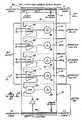
- Figure 1 illustrates, in block diagram form, one embodiment of a cell stack structure in accordance with the present invention. In particular,
cell stack 10 is seen to comprise acap cell 12 disposed at the top of a vertical stack of cells. At the bottom of the vertical stack there ispresent control cell 14. Betweencap cell 12 andcontrol cell 14 there are disposed a plurality, n, ofoperation cells 16. The number of operation cells is seen to be dependent upon the selected digit size. Each of theoperation cells 16 is operable to carry out one or more single bit operations.Cap cell 12,operation cells 16 andcontrol cell 14 are arranged in a vertical stack in which each cell is approximately the same width.Cap cell 12 is employed to carry the VSS power bus and may be used to make minor routing connections.Control cell 14 carries the VDD power bus. These power busses are typically the different polarity power conductors from a power connection which is made to the chip on whichcell stack 10 is incorporated. The cap cell and the control cell are preferably configured so as to be capable of providing a continuous conductive path connecting adjacently disposed cell stacks so that adjacently disposed cell stacks are connected to the desired power supply conductors.Control cell 14 typically carries out tasks such as delaying and resetting carry signals, buffering and inverting clock signals and performs any other necessary logic control. The function of each control cell generally varies from cell stack to cell stack. - For all cell stacks which conform to the basic template shown in Figure 1, the height of these stacks is constant. Thus, if A and B are two such cell stacks, the control cells for stacks A and B are equal in height. Similarly, the bit slices (operation cell areas) of stacks A and B are equal in height as are the cap cells. The width of the cell stacks may be different for different cell stack functions. As a result of this structure, the total cell stack height of all n bit digit serial operators is the same. The height of a cell stack is given by the following formula:
total_height = cap_height + n slice_height + control_height (1) Furthermore, power and clock signals, preferably being at standard locations in the control and cap cells provide matched connections between adjacently disposed cell stacks. Because of this, cell stacks may be placed side by side in rows of cell stacks of equal height. However, it is also possible to provide a small routing path between adjacently disposed cell stacks. This is desirable so that cells may be placed and routed with efficient standard cell place-and-route methods. - While Figure 1 shows cap cells disposed at the top of a vertical stack and control cells disposed at the bottom of this same stack, it is noted that this is not the only possible arrangement of these three different types of cells within a stack. However, it is the preferred embodiment. It is, however, noted that it would be readily possible to interchange the placement of the control cells and cap cells without significantly affecting the practice of the present invention. Similar objectives could also be obtained simply by disposing the stack cells shown in Figure 1 in an inverted position. However, in this case, the general signal flow path from one side of the stack to the other is reversed. In fact, this reversal may provide advantages in overall chip layout in which an overall signal flowpath is provided on a chip in a zigzag fashion.
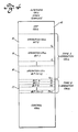
- A particular embodiment of the present invention is illustrated in Figure 2. Figure 2 illustrates, in block diagram form, a cell stack for a 4-bit digit serial adder. In particular,
cap cell 12 is seen to containpower bus 22 which is configured to readily connect adjacent cell stacks and also to provide power tooperation cells 16 and to controlcell 14. Likewise,cap cell 12 includesclock line 26 which again is readily suppliable to adjacent cells and is operable to supply clock timing signals to each ofoperation cells 16.Control cell 14 is seen to include VDDpower bus conductor 24 which is likewise readily connectable to adjacent cellstacks. Power bus 24 also supplies power, of the opposite polarity with respect topower bus 22, tooperation cells 16. - In the particular embodiment shown, a 4-bit digit serial adder is described. In particular, each
operation cell 16 includesfull adder 28 receiving digit serial inputs Ai and Bi. Here, i ranges from 0 to 3. The output of eachfull adder 28 is supplied to adelay block 32, the output of which provides digit serial output data to lines labeled XOUT₀ through XOUT₃, as shown. The carry-out signals fromfull adders 28 are supplied as inputs to the next higher significant bit. It is noted that each operation cell is the same. It is noted also that each operation cell individually performs a bit operation, but that collectively, these cells perform a 4-bit digit serial addition operation. - The digit serial adder shown in Figure 2 also includes
control cell 14 particularly configured to control the flow of carry information (at the digit level). In particular, it is seen thatcontrol cell 14 receives control signal information which is inverted byinverter 38 and supplied to ANDgate 36 which also receives high order digit carry information from thefull adder 28 which receives input signals A₃ and B₃. In operation, the control section supplies the carryout signal from the most significant bit of the digit, delays it one cycle throughdelay block 34 and returns it to the least significant digit bit in the next clock cycle. It resets it to 0 if necessary. The carry signal into the low order digit bit position is reset to 0 at the start of each data word. This reset operation is controlled by the special signal line labeled CONTROL in Figure 2 which is high only in the last digit of each data word. - In general, data words are divided into a plurality of digits, each of size n. For example, if the word size is W and the digit size is n, there will, in general, be W/n passages of information through the adder cell stack to effect the addition of two words of W bits each. It is also noted that, in Figure 2, carry
signal 21, while shown disposed in the cell stack, may also be disposed in the routing channel between adjacently disposed cell stacks (seereference numeral 45 in the discussion of Figure 3 below). - In Figure 2, it is noted that data signals are supplied from the left and outputs are taken from the righthand side of the cell stack. However, it is noted that bit operation cells may be laid out in reverse fashion with data signals being directed to the left. In fact, it may be desirable to employ both kinds of cell stacks on the same chip. That is to say, on a given chip employing the present invention, data sinals are not limited to flowing from either the left to the right or from the right to the left in a given cell stack. However, consistency in flow direction is generally advisable between adjacent disposed and connected cell stacks.
- Figure 3 illustrates a
cell stack array 50 assembled from a plurality of cell stacks 10 in accordance with the present invention. Figure 3 particularly illustrates some of the advantages of the present invention. In particular,different cell stacks 10 from a relatively small library of cell stack operators are seen to be readily configured in adjacent locations. It is seen that power busses 22 and 24 are readily connected between adjacent cell stacks 10. The same is true for theclock signal 26. Furthermore,clock signal line 26 is shown as being present incap cell 12, it is noted that it also possible to dispose a clock signal line incontrol cell 14. - A particular advantage of the cell stack configuration of the present embodiments is that the cell library does not have to contain and maintain a large number of different cell stack operators for different digit sizes. The digit size is entirely controllable simply by changing the stack height and by including the appropriate number of bit
slice operation cells 16. Thus, the configuration of the present embodiments provides an extremely flexible design without sacrificing layout efficiency. - It is noted that each of the cell stacks shown in
array 50 in Figure 3 may actually comprise different kinds of digit serial operators. Accordingly, the cell stacks are typically of varying widths even though a constant width is illustrated in Figure 3. Nonetheless, the cell stack height is substantially constant. In those signal processing applications in which data may be passed directly from one operator stack to the next, it is possible to dispose the cell stacks in substantially abutting relationships. However, in those situations in which it is desirable to re-route signal or control signal lines between cell stacks, it is desirable to employrouting channel 45 which is disposed between adjacent cell stacks. For example,signal line 21 shown in Figure 2 may in fact be disposed in one of these routing channels rather than being disposed within the operation cells. In this case, it is a matter of design choice which of the two locations forsignal line 21 is selected. It is also noted that while the stacks are oriented vertically in Figure 3, it is nonetheless possible to dispose adjacent stacks horizontally below one another. - Figure 4 illustrates an alternative cell stack template in accordance with the present invention. The template illustrated in block diagram form is similar to the template shown in Figure 1 discussed above. However, the template illustrated in Figure 4 is particularly applicable in those situations in which bit serial multiplication is performed. In particular, in Figure 4, instead of having one operation cell per bit, two such cells Ci (type 1) and Di (type 2) are employed. The cells Ci and Di are disposed in the separate stack groups in different stack positions, as shown in Figure 4. The cells Di form a stack group which performs an interleaving (rerouting) of signals (see Figure 5), whereas cells Ci (type 1) carry out single bit operations. This is done in such a way that the height h₁ of a bit slice of
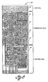
type 1 plus the height h₂ of a bit slice oftype 2 equals the height H of an operator cell in the standard template; that is, H = h₁ + h₂. One particular configuration of these interleaving data line patterns is shown in Figure 5. For example, in the construction of a multiplier for a pair of 12 bit data words, 12 cell stacks such as those shown in Figure 4 may be employed and disposed in an adjacent relationship, as in Figure 3, to perform a multiplication function. Routing of signals in the multiplication function is achieved by appropriately interleaving bit signal lines, as suggested in Figure 5. Thus, it is possible in a cell stack to employ two types of operation cells (type 1 and type 2). Nonetheless, the stack height remains the same between adjacently disposed cell stacks. Only the original design is modified to increase the operation cell number to account for the presence oftype 2operation cell 17, such as that shown in Figures 4 and 5. - Figure 6 is illustrative of an actual cell stack employed to carry out 4-bit digit serial operations such as those illustrated in block diagram form in Figure 2. It is noted, however, that Figure 6 is illustrative only and, because of the scale and the detail present in the electrical circuitry shown, the resultant depiction is generally only suggestive of the connections, layouts and transistors present. In particular, the cell stack shown performs not only additions, but also subtraction, complementation and comparison operations. Nonetheless,
cap cell 12,control cell 14 andoperation cells 16 are clearly visible in the structure seen in Figure 6. - Figure 7 illustrates yet another embodiment of the present invention. In particular, Figure 7 illustrates a cell stack template for a digit serial operator which implements a delay function. In this particular embodiment, a portion of
control cell 14 is given over to extra operation cells which extend into the control cell area. This is desirable in the situation shown in which the cell stack operation is one of delay. However, in such circumstances, control cell circuitry is generally simple and does not require the full control cell area otherwise allocated. - The circuits produced from the basic cell stack library are largely self controlled. In general, all that is necessary is that each cell stack knows when each new data word begins. Since, because of latency, the beginning of the data word varies in time from cell stack to cell stack in the circuit, each cell stack must be notified at a different time at the beginning of the data word. In order to achieve this function, control on a chip is generally centralized in a MASTER CONTROLLER cell stack which is built from bit slices according to the standard template. The MASTER CONTROLLER cell stack accepts a single input called MASTER CONTROL which may be an input to the chip directly or else may be generated internally. This MASTER CONTROL signal is generally high for one clock cycle of each sample (usually in the most significant digit, but possibly in the least significant digit) and otherwise low. Also, some cells may receive more than one differently delayed control signal. The MASTER CONTROLLER stack itself produces delayed versions of this signal. The delayed versions are the same as the input except that the high cycle is shifted in time. The properly delayed MASTER CONTROL signal is now routed to each cell stack on the chip. If the word size is W and the digit size is n, then there are W/n distinct MASTER CONTROL signals because of the periodicity of this signal. In a typical incidence, W = 16 and n = 4. In this case, there will therefore be only 4 MASTER CONTROL signals being routed around the chip. Thus, the overhead in the circuit given over to centralized control is minimal.
- It has been shown to be possible, following the cell stack architecture of the present invention, to construct libraries of cells which are easily assembled by software from a basic library of subcells, the cell stacks carry a full range of digit serial operators for arbitrary digit width. Digit widths greater than 16 are, however, generally not advisable because of the great cost of routing a circuit built from such cells. Variations on the basic template sometimes mean that cell stacks so constructed will not abut correctly with cell stacks which follow the standard template. However, this can be accommodated by corrective routing in the channels between adjacent cell stacks. The most important variation used is that instead of having a single operation cell per bit slice, each slice of an operator consists of two different cells, but still in such a way that the sum of the heights of the two subcells equals the height of a bit slice cell in a standard template. An example of this is the multiplier operator cell stack discussed above.
- From the above, it is seen that the cell stack architecture of the present embodiments is particularly usable in conjunction with silicon compilers. More particularly, however, it is seen that the present embodiments provide such compilers with the ability to employ cell libraries comprising operator cell stacks for a variable number of digit sizes. This makes optimization of digit size possible. Thus, for a given chip size, it is now possible to be able to efficiently design and lay out digital signal processing circuitry which is not fully bit serial and is not fully parallel, but utilizes an optimal digit size. It is also seen that the present embodiments provide ease of layout and high efficiency in terms of chip area utilization. It is further seen that the variable width cell stacks of the present experiments permit a silicon compiler to produce chip masks for optimum throughput circuitry for a given chip size by giving the operator a choice of digit size, a variable that has hitherto been unavailable for use in this fashion.
Claims (19)
a cap cell;
a plurality of operation cells, each of which is operable to carry out one or more single bit operations; and
a control cell;
said cap cell, said operation cells and said control cell being arranged in a stack in which each cell is approximately the same width;
said cap being configured to provide power from a first polarity supply to said operation cells and to provide a conductive path connecting adjacently disposed cell stacks so that said adjacently disposed cell stacks are connected to said first polarity supply;
said control cell being configured to provide power from a second polarity supply to said operation cells and to provide a conductive path connecting adjacently disposed cell stacks so that said adjacently disposed cell stacks are connected to said second polarity supply.
Applications Claiming Priority (2)
| Application Number | Priority Date | Filing Date | Title |
|---|---|---|---|
| US07/182,602 US4951221A (en) | 1988-04-18 | 1988-04-18 | Cell stack for variable digit width serial architecture |
| US182602 | 1994-01-14 |
Publications (3)
| Publication Number | Publication Date |
|---|---|
| EP0338757A2 true EP0338757A2 (en) | 1989-10-25 |
| EP0338757A3 EP0338757A3 (en) | 1992-01-15 |
| EP0338757B1 EP0338757B1 (en) | 1996-01-03 |
Family
ID=22669188
Family Applications (1)
| Application Number | Title | Priority Date | Filing Date |
|---|---|---|---|
| EP89303799A Expired - Lifetime EP0338757B1 (en) | 1988-04-18 | 1989-04-17 | A cell stack for variable digit width serial architecture |
Country Status (4)
| Country | Link |
|---|---|
| US (1) | US4951221A (en) |
| EP (1) | EP0338757B1 (en) |
| JP (1) | JPH0216631A (en) |
| DE (1) | DE68925303T2 (en) |
Families Citing this family (13)
| Publication number | Priority date | Publication date | Assignee | Title |
|---|---|---|---|---|
| US5084834A (en) * | 1988-04-18 | 1992-01-28 | General Electric Company | Digit-serial linear combining apparatus |
| US5283753A (en) * | 1991-07-25 | 1994-02-01 | Motorola, Inc. | Firm function block for a programmable block architected heterogeneous integrated circuit |
| JP3479538B2 (en) * | 1991-12-26 | 2003-12-15 | テキサス インスツルメンツ インコーポレイテツド | Method of manufacturing semiconductor integrated circuit |
| JP3224885B2 (en) * | 1993-01-14 | 2001-11-05 | 三菱電機株式会社 | Integrated circuit device and design method thereof |
| US5623684A (en) * | 1994-05-17 | 1997-04-22 | Commquest Technologies, Inc. | Application specific processor architecture comprising pre-designed reconfigurable application elements interconnected via a bus with high-level statements controlling configuration and data routing |
| JP3599368B2 (en) * | 1994-05-20 | 2004-12-08 | 株式会社ルネサステクノロジ | Parallel processing microprocessor |
| US5867400A (en) * | 1995-05-17 | 1999-02-02 | International Business Machines Corporation | Application specific processor and design method for same |
| US5838583A (en) * | 1996-04-12 | 1998-11-17 | Cadence Design Systems, Inc. | Optimized placement and routing of datapaths |
| US6090151A (en) * | 1997-07-01 | 2000-07-18 | Motorola, Inc. | Electronic device parameter estimator and method therefor |
| US6230175B1 (en) | 1997-11-11 | 2001-05-08 | Matsushita Electric Industrial Co., Ltd. | Reconfigurable digit-serial arithmetic system having a plurality of digit-serial arithmetic units |
| US6502231B1 (en) | 2001-05-31 | 2002-12-31 | Applied Micro Circuits Corporation | Integrated circuit template cell system and method |
| GB2376819A (en) * | 2001-06-21 | 2002-12-24 | Ericsson Telefon Ab L M | Electronic circuit having series connected circuit blocks |
| JP2004153138A (en) * | 2002-10-31 | 2004-05-27 | Renesas Technology Corp | Semiconductor integrated circuit |
Citations (1)
| Publication number | Priority date | Publication date | Assignee | Title |
|---|---|---|---|---|
| EP0182041A2 (en) * | 1984-11-15 | 1986-05-28 | International Business Machines Corporation | Integrated circuit chip with "bit-stacked" functional blocks |
Family Cites Families (5)
| Publication number | Priority date | Publication date | Assignee | Title |
|---|---|---|---|---|
| US4739474A (en) * | 1983-03-10 | 1988-04-19 | Martin Marietta Corporation | Geometric-arithmetic parallel processor |
| US4584653A (en) * | 1983-03-22 | 1986-04-22 | Fujitsu Limited | Method for manufacturing a gate array integrated circuit device |
| US4621339A (en) * | 1983-06-13 | 1986-11-04 | Duke University | SIMD machine using cube connected cycles network architecture for vector processing |
| US4701860A (en) * | 1985-03-07 | 1987-10-20 | Harris Corporation | Integrated circuit architecture formed of parametric macro-cells |
| US4791590A (en) * | 1985-11-19 | 1988-12-13 | Cornell Research Foundation, Inc. | High performance signal processor |
-
1988
- 1988-04-18 US US07/182,602 patent/US4951221A/en not_active Expired - Lifetime
-
1989
- 1989-04-17 DE DE68925303T patent/DE68925303T2/en not_active Expired - Fee Related
- 1989-04-17 EP EP89303799A patent/EP0338757B1/en not_active Expired - Lifetime
- 1989-04-17 JP JP1095469A patent/JPH0216631A/en active Pending
Patent Citations (1)
| Publication number | Priority date | Publication date | Assignee | Title |
|---|---|---|---|---|
| EP0182041A2 (en) * | 1984-11-15 | 1986-05-28 | International Business Machines Corporation | Integrated circuit chip with "bit-stacked" functional blocks |
Non-Patent Citations (3)
| Title |
|---|
| 25TH ACM/IEEE DESIGN AUTOMATION CONFERENCE June 1988, ANAHEIM CONVENTION CENTER US pages 646 - 649; R.I. HARTLEY: 'a digit-serial silicon compiler' whole document * |
| PROCEEDINGS OF THE IEEE 1986 CUSTOM INTEGRATED CIRCUITS CONFERENCE May 1986, NEW YORK US pages 10 - 14; R.C MASON ET AL: 'a bit-modular cell library optimised for data-path applications' * |
| PROCEEDINGS OF THE IEEE. vol. 75, no. 9, September 1987, NEW YORK US pages 1272 - 1281; F.F.YASSA ET AL: 'silicon compiler for digital signal processing : methodology, implementation, and applications' * |
Also Published As
| Publication number | Publication date |
|---|---|
| DE68925303T2 (en) | 1996-08-29 |
| DE68925303D1 (en) | 1996-02-15 |
| US4951221A (en) | 1990-08-21 |
| JPH0216631A (en) | 1990-01-19 |
| EP0338757A3 (en) | 1992-01-15 |
| EP0338757B1 (en) | 1996-01-03 |
Similar Documents
| Publication | Publication Date | Title |
|---|---|---|
| US5243238A (en) | Configurable cellular array | |
| Hartley et al. | Digit-serial processing techniques | |
| US7346644B1 (en) | Devices and methods with programmable logic and digital signal processing regions | |
| US6771094B1 (en) | Devices and methods with programmable logic and digital signal processing regions | |
| Mirsky et al. | MATRIX: a reconfigurable computing architecture with configurable instruction distribution and deployable resources | |
| US8058899B2 (en) | Logic cell array and bus system | |
| US6553395B2 (en) | Reconfigurable processor devices | |
| Jacobs et al. | A fully asynchronous digital signal processor using self-timed circuits | |
| US7595659B2 (en) | Logic cell array and bus system | |
| Singh et al. | PITIA: an FPGA for throughput-intensive applications | |
| EP0338757B1 (en) | A cell stack for variable digit width serial architecture | |
| EP0908887A3 (en) | Semiconductor integrated circuit device | |
| US20070124565A1 (en) | Reconfigurable processing array having hierarchical communication network | |
| US7119576B1 (en) | Devices and methods with programmable logic and digital signal processing regions | |
| EP0079127A1 (en) | Programmable system component | |
| US6769007B2 (en) | Adder circuit with a regular structure | |
| CN213042269U (en) | Computing chip, computing force plate and digital currency mining machine | |
| Bekhale et al. | Reconfiguration strategies for VLSI processor arrays and trees using a modified Diogenes approach | |
| Ebeling et al. | Triptych: A new FPGA architecture | |
| CN114442996A (en) | Computing chip, computing force plate and digital currency mining machine | |
| Pang | Architectures for pipelined Wallace tree multiplier-accumulators | |
| Louie et al. | A variable-precision square root implementation for field programmable gate arrays | |
| Hartley et al. | Rapid prototyping using high density interconnects | |
| US9626325B2 (en) | Array processor having a segmented bus system | |
| KR950009773B1 (en) | Method of arranging unit circuit in a mesh type parallel computer |
Legal Events
| Date | Code | Title | Description |
|---|---|---|---|
| PUAI | Public reference made under article 153(3) epc to a published international application that has entered the european phase |
Free format text: ORIGINAL CODE: 0009012 |
|
| AK | Designated contracting states |
Kind code of ref document: A2 Designated state(s): DE FR GB IT NL |
|
| PUAL | Search report despatched |
Free format text: ORIGINAL CODE: 0009013 |
|
| AK | Designated contracting states |
Kind code of ref document: A3 Designated state(s): DE FR GB IT NL |
|
| 17P | Request for examination filed |
Effective date: 19911220 |
|
| 17Q | First examination report despatched |
Effective date: 19940601 |
|
| GRAA | (expected) grant |
Free format text: ORIGINAL CODE: 0009210 |
|
| RAP1 | Party data changed (applicant data changed or rights of an application transferred) |
Owner name: HARRIS CORPORATION |
|
| AK | Designated contracting states |
Kind code of ref document: B1 Designated state(s): DE FR GB IT NL |
|
| PG25 | Lapsed in a contracting state [announced via postgrant information from national office to epo] |
Ref country code: NL Free format text: LAPSE BECAUSE OF FAILURE TO SUBMIT A TRANSLATION OF THE DESCRIPTION OR TO PAY THE FEE WITHIN THE PRESCRIBED TIME-LIMIT Effective date: 19960103 |
|
| ET | Fr: translation filed | ||
| REF | Corresponds to: |
Ref document number: 68925303 Country of ref document: DE Date of ref document: 19960215 |
|
| ITF | It: translation for a ep patent filed |
Owner name: MODIANO & ASSOCIATI S.R.L. |
|
| NLT2 | Nl: modifications (of names), taken from the european patent patent bulletin |
Owner name: HARRIS CORPORATION |
|
| NLV1 | Nl: lapsed or annulled due to failure to fulfill the requirements of art. 29p and 29m of the patents act | ||
| PLBE | No opposition filed within time limit |
Free format text: ORIGINAL CODE: 0009261 |
|
| STAA | Information on the status of an ep patent application or granted ep patent |
Free format text: STATUS: NO OPPOSITION FILED WITHIN TIME LIMIT |
|
| 26N | No opposition filed | ||
| PGFP | Annual fee paid to national office [announced via postgrant information from national office to epo] |
Ref country code: FR Payment date: 19980319 Year of fee payment: 10 |
|
| PGFP | Annual fee paid to national office [announced via postgrant information from national office to epo] |
Ref country code: GB Payment date: 19980325 Year of fee payment: 10 |
|
| PGFP | Annual fee paid to national office [announced via postgrant information from national office to epo] |
Ref country code: DE Payment date: 19980326 Year of fee payment: 10 |
|
| PG25 | Lapsed in a contracting state [announced via postgrant information from national office to epo] |
Ref country code: GB Free format text: LAPSE BECAUSE OF NON-PAYMENT OF DUE FEES Effective date: 19990417 |
|
| GBPC | Gb: european patent ceased through non-payment of renewal fee |
Effective date: 19990417 |
|
| PG25 | Lapsed in a contracting state [announced via postgrant information from national office to epo] |
Ref country code: FR Free format text: LAPSE BECAUSE OF NON-PAYMENT OF DUE FEES Effective date: 19991231 |
|
| REG | Reference to a national code |
Ref country code: FR Ref legal event code: ST |
|
| PG25 | Lapsed in a contracting state [announced via postgrant information from national office to epo] |
Ref country code: DE Free format text: LAPSE BECAUSE OF NON-PAYMENT OF DUE FEES Effective date: 20000201 |
|
| PGFP | Annual fee paid to national office [announced via postgrant information from national office to epo] |
Ref country code: IT Payment date: 20080429 Year of fee payment: 20 |