EP0341989A2 - Apparatus for simultaneously outputting plural image signals derived from a video signal, comprising a single digital-to- analogue converter - Google Patents
Apparatus for simultaneously outputting plural image signals derived from a video signal, comprising a single digital-to- analogue converter Download PDFInfo
- Publication number
- EP0341989A2 EP0341989A2 EP89304701A EP89304701A EP0341989A2 EP 0341989 A2 EP0341989 A2 EP 0341989A2 EP 89304701 A EP89304701 A EP 89304701A EP 89304701 A EP89304701 A EP 89304701A EP 0341989 A2 EP0341989 A2 EP 0341989A2
- Authority
- EP
- European Patent Office
- Prior art keywords
- signal
- analog
- digital
- circuit
- holding
- Prior art date
- Legal status (The legal status is an assumption and is not a legal conclusion. Google has not performed a legal analysis and makes no representation as to the accuracy of the status listed.)
- Granted
Links
Images


Classifications
-
- H—ELECTRICITY
- H04—ELECTRIC COMMUNICATION TECHNIQUE
- H04N—PICTORIAL COMMUNICATION, e.g. TELEVISION
- H04N9/00—Details of colour television systems
- H04N9/64—Circuits for processing colour signals
Definitions
- the invention relates to an output apparatus for image signals, and more particularly to an output apparatus for image signals applicable to a TV (television), a VTR (video-tape-recorder), a VTR camera etc. from which plural output signals are supplied to a following stage.
- the conventional output apparatus for image signals comprises an image signal processing circuit for digital-processing input image signals to provide a luminance signal and a composite video signal, and D/A converters for converting the digital luminance and composite video signals to analog luminance and composite video signals, respectively.
- the digital luminance signal is used as a black-and white-video signal for a view finder, and the composite video signal is used as a main output.
- Such an image signal processing circuit is described on pages 372 to 378 of "IEEE Transactions on Consumer Electronics, Vol. CE-32, No. 3, August 1986".
- the conventional output apparatus for image signals is difficult to be included in a single integration circuit because the number of D/A converters is increased to result in the increase of the number of input and output terminals. As a result, the size of the conventional output apparatus for image signals becomes large.
- an output apparatus for image signals comprises, an image signal processing circuit for providing a digital luminance signal, and at least one signal selected from a digital color signal and a digital composite video signal in accordance with a digital processing of image signals supplied from a signal input terminal; a multiplexing circuit for multiplexing said digital luminance signal and said at least one signal to be positioned alternately on a time axis; a D/A converter for converting a digital output signal of said multiplexing circuit to an analog multiplexed signal; and at least two signal holding circuits for holding said analog multiplexed signal which is separated into an analog luminance signal and an analog signal corresponding to said at least one signal, one of said at least two signal holding circuits being connected to a signal output terminal and holding said analog luminance signal, and the other of said at least two signal holding circuits being connected to another signal output terminal and holding said analog signal.
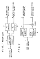
- Fig. 1 shows the output apparatus for image signals which comprises an image signal processing circuit 2 for digital-processing image signals supplied to an image signal input terminal 1 to provide a luminans signal and a composite video signal, a D/A converter 11 for converting the digital luminans signal to an analog luminans signal which is supplied to an luminous signal output terminal 7, and a D/A converter 12 for converting the digital composite video signal to an analog composite video signal which is supplied to a composite video signal output terminal 8.
- an image signal processing circuit 2 for digital-processing image signals supplied to an image signal input terminal 1 to provide a luminans signal and a composite video signal
- a D/A converter 11 for converting the digital luminans signal to an analog luminans signal which is supplied to an luminous signal output terminal 7
- a D/A converter 12 for converting the digital composite video signal to an analog composite video signal which is supplied to a composite video signal output terminal 8.
- Fig. 2 shows the image signal processing circuit 2 which comprises a luminance signal processing circuit 13 for digital-calculating luminance signals to provide the digital luminance signal which is a black-and white-monitoring signal, a color signal processing circuit 14 for digital-calculating color signals to provide the digital color signal, an adder 17 for adding the digital luminance signal and the color signal to provide the digital composite video signal, and output terminals 15 and 16, respectively, connected to the D/A converters 11 and 12.
- image signals are supplied to the image signal input terminal 1, and then processed in the image signal processing circuit 2.
- the luminance signal is supplied from the luminance signal processing circuit 13 to the adder 17 and through the luminance signal output terminal 15 to the D/A converter 11, and the color signal is supplied from the color signal processing circuit 14 to the adder 17.
- the luminance signal and the color signal are added to provide the composite video signal which is supplied therefrom through the composite video signal output terminal 16 to the D/A converter 12.
- the digital luminance signal and the digital composite video signal are converted to the analog luminance signal and the analog composite video signal, respectively.
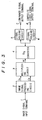
- the output apparatus for image signals comprises an image signal processing circuit 2 for digital-processing image signals supplied to an image signal input terminal 1, a multiplexing circuit 3 for multiplexing a digital luminance signal and a digital composite video signal, respectively, supplied from the image signal processing circuit 2, a D/A converter 4 for converting the digital luminance signal and the digital composite video signal in time-division to an analog luminance signal and an analog composite video signal, and signal holding circuits 5 and 6 for holding the analog luminance and composite video signals which are supplied to luminance and composite video signal output terminals 7 and 8, respectively.
- image signals are supplied to the image signal input terminal 1, and then processed in the image signal processing circuit 2, for instance, as explained in Fig. 2, so that a luminance signal Y D (Y1, Y2, ... ) and a composite video signal C D (C1, C2, ...) are supplied in serial digital data trains to the multiplexing circuit 3 as shown in Fig. 4.
- Each of the digital data Y1, Y2 ... and C1, C2 ... is of several bits forming a serial or parallel signal.
- the luminance and composite video signals Y D and C D are multiplexed serially in the multiplexing circuit 3 to provide a multiplexed signal M in which the two signals are positioned alternately one after another as shown in Fig. 4.
- the multiplexed signal M is converted from digital to analog in the D/A converter 4, so that the analog luminance signal Y A (Y1, Y2, ... ) and the analog composite video signal C A (C1, C2, ... ) are supplied alternately to the signal holding circuits 5 and 6 in which the two signals are held correspondingly.
- the analog luminance signal Y A and the analog composite video signal C A are supplied through the output terminals 7 and 8 to a following stage, respectively, as shown in Fig. 4.
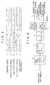
- Fig. 5 shows an output apparatus for image signals in a second embodiment according to the invention.
- the output apparatus for image signals like parts are indicated by like reference numerals in Fig. 3, provided that the image signal processing circuit 2 does not include the aforementioned adder 17, but the luminance signal processing circuit 13 and the color signal processing circuit 14 as shown in Fig. 2.
- the output apparatus for image signals comprises an adder 10 provided between outputs of the signal holding circuits 5 and 6 and connected to the composite video signal output terminal 8. Furthermore, the signal holding circuits 5 and 6 are connected to luminance and color signal output terminals 7 and 9.
- image signals are supplied to the image signal input terminal 1, and then processed in the image signal processing circuit 2 to provide a digital luminance signal and a digital color signal which are multiplexed serially in the multiplexing circuit 3 to provide a digital multiplexed signal.
- the digital multiplexed signal is converted in the D/A converter 4 to an analog multiplexed signal which is separated into an analog luminance signal and an analog color signal sequentially, and the analog luminance signal is held in the signal holding circuit 5, while the analog color signal is held in the signal holding circuit 6.
- the analog luminance and color signals supplied from the signal holding circuits 5 and 6 are added in the adder 10 to provide a composite video signal supplied to the composite video signal output terminal 8.
- the analog luminance and color signals are directly supplied to the luminance and color signal output terminals 7 and 9, respectively.
- the object of the invention in which the number of D/A converters is decreased is realized.
- a following disadvantage is desired to be overcome in the invention. This will be explained in the output apparatus for image signals in the second embodiment.
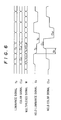
- Fig. 6 shows the digital luminance signal Y D , the digital color signal CL D , the digital multiplexed signal M, the analog luminance signal Y A , and the analog color signal CL A .
- the digital luminance signal Y1 corresponds to the digital color signal CL1 in a relation of signal produced in an image at the same time, and the digital luminance signal Y2 to the digital color signal CL2.
- These signals Y1, CL1, Y2, CL2, ... are multiplexed serially to provide the digital multiplexed signal M, such that the corresponding signals Y1 and CL1, Y2 and CL2, ... are arranged at different positions on a time axis.
- Fig. 7 shows an output apparatus for image signals in the third embodiment in which like parts are indicated by like reference numerals in Fig. 5, provided that the adder 10 is not provided therein, but a delay circuit 29 is provided between the image signal processing circuit 2 and the multiplexing circuit 3, and a filter 30 is provided between the signal holding circuit 6 and the color signal output terminal 9.
- image signals are supplied to the image signal input terminal 1, and then processed in the image signal processing circuit 2 to provide a digital luminance signal Y D1 (Y1, Y2, ... ) and a digital color signal CL D (CL1, CL1, ... ), wherein the data Y1, Y2... correspond to the data CL1, CL2 ..., respectively, on a time axis, as shown in Fig. 8.
- the digital luminance signal Y D1 is delayed in the delay circuit 29 by a time equal to the length of three data, so that a digital luminance signal Y D2 (Y1, Y2, ... ) is obtained as shown in Fig. 8.
- the digital luminance signal Y D2 and the digital color signal CL D are multiplexed in the multiplexing circuit 3 to provide a digital multiplexed signal which is then converted to an analog multiplexed signal, so that the analog multiplexed signal is separated into an analog luminance signal Y A and an analog color signal CL A1 which are then held in the signal holding circuits 5 and 6, respectively, in the same manner as explained in the first and second embodiments.
- the luminance data Y1, Y2, ... are delayed by a time equal to the length of one datum in the multiplexing circuit 3 and the D/A converter 4, while the color data CL1, CL2 ... are delayed by a time equal to the length of one and half data as shown in Fig. 8.
- a time difference of two and half data occurs between the analog luminance signal Y A and the analog color signal CL A1 .
- the analog color signal CL A1 is passed through the filter 30 to receive a band limitation of the color signal. Consequently, the analog color signal CL A1 is delayed by a time equal to the length of two and half data, so that the analog luminance signal Y A and the analog color signal CL A2 are supplied to the luminance signal output terminal 7 and the color signal output terminal 9, respectively, which are restored with a synchronous time relation as shown in Fig. 8.
- the delay time of the filter 30 is a time equal to the length of two and half data in the third embodiment, it may be changed dependent on a circuitry structure.
- the delay time of the delay circuit 29 may be changed in compliance with a changed delay time of the filter 30. Since the delay circuit 29 is of a digital type, it is easy to provide a predetermined amount of a time delay based on a unit which is one datum.
- a time which is delayed in the filter 30 deviates in a period less than the length of one datum, for instance, where a time which is half a datum deviates in a delay of three data, such a deviation can not be compensated by the delay circuit 29.
- a signal holding unit as shown in Fig. 9 is used for the compensation of the delay time deviation.
- Fig. 9 shows the signal holding unit which comprises first and second sample holding circuits 33 and 34, and an inverter 16, wherein an input of the first sample holding circuit 33 is connected to a signal input terminal 31, an output of the first sample holding circuit 33 is connected to an input of the second sample holding circuit 34, and an output of the second sample holding circuit 34 is connected to a signal output terminal 35. Furthermore, the first sample holding circuit 33 operates in accordance with clocks supplied from a clock input terminal 32, and the second sample holding circuit 34 operates in accordance with inverted clocks supplied from the inverter 36 which is connected to the clock input terminal 32.
- signals which are supplied to the signal input terminal 31 are to be held in the first sample holding circuit 33 in accordance with the clocks applied to the clock input terminal 32, and signals which are held in the first sample holding circuit 33 are to be held in the second sample holding circuit 34 in accordance with the inverted clocks supplied from the inverter 36, so that signals at the signal output terminal 35 are delayed by a half clock rate as compared to those which appear at the signal output terminal 35 where only the first sample holding circuit 33 is provided.
- a time equal to a half datum period is delayed under a condition that one clock rate is one datum period.
- Fig. 10 shows a timing chart in operation, wherein the signal holding unit of Fig. 9 is used as the signal holding circuit 5 in the output apparatus for image signals of Fig. 7, which includes the filter 30 having a delay time equal to the length of three data.
- the analog color signal CL A2 is delayed behind the analog color signal CL A1 by a delay time of the filter 30 equal to three data, and is delayed behind the analog luminance signal Y A1 supplied from the D/A converter 7 by a half datum period.
- the analog luminance signal Y A2 passed through the signal holding circuit 5 (the same as the signal holding unit as shown in Fig. 9) is delayed by a half datume period, so that the analog luminance signal Y A2 appearing at the signal output terminal 7 is corrected to coincide with the analog color signal CL A2 on a time axis.
- Fig. 11 shows an output apparatus for image signals in a fourth embodiment according to the invention.
- the output apparatus for image signals is the same as that in the third embodiment, except that an adder 10 is further provided.
- First and second inputs of the adder 10 are connected to outputs of the signal holding circuit 5 and the filter 30, respectively, and an output of the adder is connected to a composite video signal output terminal 8.
- an analog luminance signal of the signal holding circuit 5 and an analog color signal of the filter 30 are supplied to the luminance signal output terminal 7 and the color signal output terminal 9, respectively, and are added in the adder 10 to provide a composite video signal which is supplied to the composite video signal output terminal 8.
- transmitting and receiving of image signals are carried out in image apparatus by use of a composite video signal.
- a time deviation between a luminance signal and a color signal must be suppressed, and band limitations for the both signals become strict.
- the invention is very advantageous.
Abstract
Description
- The invention relates to an output apparatus for image signals, and more particularly to an output apparatus for image signals applicable to a TV (television), a VTR (video-tape-recorder), a VTR camera etc. from which plural output signals are supplied to a following stage.
- One type of a conventional output apparatus for image signals is described on pages 21 and 22 of "the television institute's technical report, TEBS 96-5 May 24, 1984". The conventional output apparatus for image signals comprises an image signal processing circuit for digital-processing input image signals to provide a luminance signal and a composite video signal, and D/A converters for converting the digital luminance and composite video signals to analog luminance and composite video signals, respectively. In a VTR camera, for instance, the digital luminance signal is used as a black-and white-video signal for a view finder, and the composite video signal is used as a main output. Such an image signal processing circuit is described on pages 372 to 378 of "IEEE Transactions on Consumer Electronics, Vol. CE-32, No. 3, August 1986".
- In the conventional output apparatus for image signals, however, there is a disadvantage that D/A converters must be provided by the number equal to that of output signals such as the luminance signal, and the composite video signal. Therefore, the cost of the conventional output apparatus for image signals is difficult to be decreased because a D/A converter is high in cost as compared to other circuits. It tends that the number of D/A converters is increased because output signals such as signals separated from a luminance signal and a color modulated signal, a line sequential signal etc. are produced in addition to the black-and white-monitoring signal and the composite video signal as described before.
- There is a further disadvantage that the conventional output apparatus for image signals is difficult to be included in a single integration circuit because the number of D/A converters is increased to result in the increase of the number of input and output terminals. As a result, the size of the conventional output apparatus for image signals becomes large.
- Accordingly, it is an object of the invention to provide an output apparatus for image signals in which the number of D/A converters is decreased, thereby resulting in the decrease of the cost.
- It is a further object of the invention to provide an output apparatus for image signals, the size of which is suppressed to be large.
- According to the invention, an output apparatus for image signals: comprises,
an image signal processing circuit for providing a digital luminance signal, and at least one signal selected from a digital color signal and a digital composite video signal in accordance with a digital processing of image signals supplied from a signal input terminal;
a multiplexing circuit for multiplexing said digital luminance signal and said at least one signal to be positioned alternately on a time axis;
a D/A converter for converting a digital output signal of said multiplexing circuit to an analog multiplexed signal; and
at least two signal holding circuits for holding said analog multiplexed signal which is separated into an analog luminance signal and an analog signal corresponding to said at least one signal, one of said at least two signal holding circuits being connected to a signal output terminal and holding said analog luminance signal, and the other of said at least two signal holding circuits being connected to another signal output terminal and holding said analog signal. - The invention will be explained in more detail in conjunction with appended drawings: wherein,
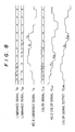
- Fig. 1 is a block diagram showing a conventional output apparatus for image signals,
- Fig. 2 is a block diagram showing an image signal processing circuit which is used in the conventional output apparatus for image signals as shown in Fig. 1,
- Fig. 3 is a block diagram showing an output apparatus for image signals in a first embodiment according to the invention,
- Fig. 4 is a timing chart explaining operation of the first embodiment,
- Fig. 5 is a block diagram showing an output apparatus for image signals in a second embodiment according to the invention,
- Fig. 6 is a timing chart explaining operation of the second embodiment,
- Fig. 7 is a block diagram showing an output apparatus for image signals in a third embodiment according to the invention,
- Fig. 8 is a timing chart explaining operation of the third embodiment,
- Fig. 9 is a block diagram showing a signal holding circuit which is used in the third embodiment,
- Fig. 10 is a timing chart explaining operation of the third embodiment in which the signal holding circuit is used as shown in Fig. 9, and
- Fig. 11 is a block diagram showing an output apparatus for image signals in a fourth embodiment according to the invention.
- Before explaining an output apparatus for image signals according to the invention, the aforementioned conventional output apparatus for image signals will be explained.
- Fig. 1 shows the output apparatus for image signals which comprises an image
signal processing circuit 2 for digital-processing image signals supplied to an image signal input terminal 1 to provide a luminans signal and a composite video signal, a D/A converter 11 for converting the digital luminans signal to an analog luminans signal which is supplied to an luminous signal output terminal 7, and a D/A converter 12 for converting the digital composite video signal to an analog composite video signal which is supplied to a composite videosignal output terminal 8. - Fig. 2 shows the image
signal processing circuit 2 which comprises a luminancesignal processing circuit 13 for digital-calculating luminance signals to provide the digital luminance signal which is a black-and white-monitoring signal, a colorsignal processing circuit 14 for digital-calculating color signals to provide the digital color signal, an adder 17 for adding the digital luminance signal and the color signal to provide the digital composite video signal, andoutput terminals A converters - In operation, image signals are supplied to the image signal input terminal 1, and then processed in the image
signal processing circuit 2. In the imagesignal processing circuit 2, the luminance signal is supplied from the luminancesignal processing circuit 13 to the adder 17 and through the luminancesignal output terminal 15 to the D/A converter 11, and the color signal is supplied from the colorsignal processing circuit 14 to the adder 17. In the adder 17, the luminance signal and the color signal are added to provide the composite video signal which is supplied therefrom through the composite videosignal output terminal 16 to the D/A converter 12. In the D/A converters - The aforementioned disadvantages of the conventional output apparatus for image signals are not explained here.
- Next, an output apparatus for image signals in a first embodiment according to the invention will be explained in Fig. 3. The output apparatus for image signals comprises an image
signal processing circuit 2 for digital-processing image signals supplied to an image signal input terminal 1, amultiplexing circuit 3 for multiplexing a digital luminance signal and a digital composite video signal, respectively, supplied from the imagesignal processing circuit 2, a D/A converter 4 for converting the digital luminance signal and the digital composite video signal in time-division to an analog luminance signal and an analog composite video signal, andsignal holding circuits signal output terminals 7 and 8, respectively. - In operation, image signals are supplied to the image signal input terminal 1, and then processed in the image
signal processing circuit 2, for instance, as explained in Fig. 2, so that a luminance signal YD (Y₁, Y₂, ... ) and a composite video signal CD (C₁, C₂, ...) are supplied in serial digital data trains to themultiplexing circuit 3 as shown in Fig. 4. Each of the digital data Y₁, Y₂ ... and C₁, C₂ ... is of several bits forming a serial or parallel signal. The luminance and composite video signals YD and CD are multiplexed serially in themultiplexing circuit 3 to provide a multiplexed signal M in which the two signals are positioned alternately one after another as shown in Fig. 4. The multiplexed signal M is converted from digital to analog in the D/A converter 4, so that the analog luminance signal YA (Y₁, Y₂, ... ) and the analog composite video signal CA (C₁, C₂, ... ) are supplied alternately to thesignal holding circuits output terminals 7 and 8 to a following stage, respectively, as shown in Fig. 4. - Fig. 5 shows an output apparatus for image signals in a second embodiment according to the invention. In the output apparatus for image signals, like parts are indicated by like reference numerals in Fig. 3, provided that the image
signal processing circuit 2 does not include the aforementioned adder 17, but the luminancesignal processing circuit 13 and the colorsignal processing circuit 14 as shown in Fig. 2. Instead, the output apparatus for image signals comprises anadder 10 provided between outputs of thesignal holding circuits signal output terminal 8. Furthermore, thesignal holding circuits signal output terminals 7 and 9. - In operation, image signals are supplied to the image signal input terminal 1, and then processed in the image
signal processing circuit 2 to provide a digital luminance signal and a digital color signal which are multiplexed serially in themultiplexing circuit 3 to provide a digital multiplexed signal. Then, the digital multiplexed signal is converted in the D/A converter 4 to an analog multiplexed signal which is separated into an analog luminance signal and an analog color signal sequentially, and the analog luminance signal is held in thesignal holding circuit 5, while the analog color signal is held in thesignal holding circuit 6. The analog luminance and color signals supplied from thesignal holding circuits adder 10 to provide a composite video signal supplied to the composite videosignal output terminal 8. At the same time, the analog luminance and color signals are directly supplied to the luminance and colorsignal output terminals 7 and 9, respectively. - In the first and second embodiments, the object of the invention in which the number of D/A converters is decreased is realized. In addition, a following disadvantage is desired to be overcome in the invention. This will be explained in the output apparatus for image signals in the second embodiment.
- Fig. 6 shows the digital luminance signal YD, the digital color signal CLD, the digital multiplexed signal M, the analog luminance signal YA, and the analog color signal CLA. In Fig. 6, the digital luminance signal Y₁ corresponds to the digital color signal CL₁ in a relation of signal produced in an image at the same time, and the digital luminance signal Y₂ to the digital color signal CL₂. These signals Y₁, CL₁, Y₂, CL₂, ... are multiplexed serially to provide the digital multiplexed signal M, such that the corresponding signals Y₁ and CL₁, Y₂ and CL₂, ... are arranged at different positions on a time axis. Consequently, a time deviation "td" which is equal to a time duration of the multiplexed luminance signal Y₁, Y₂, ... or the multiplexed color signal CL₁, CL₂ ... is resulted between the analog luminance signal Y₁, Y₂ ... and the analog color signal CL₁, CL₂, ....
- Furthermore, it is often adopted that a band limitation is applied to the color signal by use of a bandpass filter. In such a case, the time deviation "td" is increased due to a time delay induced in the bandpass filter. This disadvantage is overcome in a third embodiment which will be explained in Fig. 7. The same time delay is also observed in Fig. 4.
- Fig. 7 shows an output apparatus for image signals in the third embodiment in which like parts are indicated by like reference numerals in Fig. 5, provided that the
adder 10 is not provided therein, but adelay circuit 29 is provided between the imagesignal processing circuit 2 and themultiplexing circuit 3, and afilter 30 is provided between thesignal holding circuit 6 and the colorsignal output terminal 9. - In operation, image signals are supplied to the image signal input terminal 1, and then processed in the image
signal processing circuit 2 to provide a digital luminance signal YD1 (Y₁, Y₂, ... ) and a digital color signal CLD (CL₁, CL₁, ... ), wherein the data Y₁, Y₂... correspond to the data CL₁, CL₂ ..., respectively, on a time axis, as shown in Fig. 8. The digital luminance signal YD1 is delayed in thedelay circuit 29 by a time equal to the length of three data, so that a digital luminance signal YD2 (Y₁, Y₂, ... ) is obtained as shown in Fig. 8. Thereafter, the digital luminance signal YD2 and the digital color signal CLD are multiplexed in themultiplexing circuit 3 to provide a digital multiplexed signal which is then converted to an analog multiplexed signal, so that the analog multiplexed signal is separated into an analog luminance signal YA and an analog color signal CLA1 which are then held in thesignal holding circuits multiplexing circuit 3 and the D/A converter 4, while the color data CL₁, CL₂ ... are delayed by a time equal to the length of one and half data as shown in Fig. 8. As a result, a time difference of two and half data occurs between the analog luminance signal YA and the analog color signal CLA1. The analog color signal CLA1 is passed through thefilter 30 to receive a band limitation of the color signal. Consequently, the analog color signal CLA1 is delayed by a time equal to the length of two and half data, so that the analog luminance signal YA and the analog color signal CLA2 are supplied to the luminance signal output terminal 7 and the colorsignal output terminal 9, respectively, which are restored with a synchronous time relation as shown in Fig. 8. - Although the delay time of the
filter 30 is a time equal to the length of two and half data in the third embodiment, it may be changed dependent on a circuitry structure. As a matter of course, the delay time of thedelay circuit 29 may be changed in compliance with a changed delay time of thefilter 30. Since thedelay circuit 29 is of a digital type, it is easy to provide a predetermined amount of a time delay based on a unit which is one datum. On the other hand, where a time which is delayed in thefilter 30 deviates in a period less than the length of one datum, for instance, where a time which is half a datum deviates in a delay of three data, such a deviation can not be compensated by thedelay circuit 29. In such a case, a signal holding unit as shown in Fig. 9 is used for the compensation of the delay time deviation. - Fig. 9 shows the signal holding unit which comprises first and second
sample holding circuits inverter 16, wherein an input of the firstsample holding circuit 33 is connected to asignal input terminal 31, an output of the firstsample holding circuit 33 is connected to an input of the secondsample holding circuit 34, and an output of the secondsample holding circuit 34 is connected to asignal output terminal 35. Furthermore, the firstsample holding circuit 33 operates in accordance with clocks supplied from aclock input terminal 32, and the secondsample holding circuit 34 operates in accordance with inverted clocks supplied from theinverter 36 which is connected to theclock input terminal 32. - In operation, signals which are supplied to the
signal input terminal 31 are to be held in the firstsample holding circuit 33 in accordance with the clocks applied to theclock input terminal 32, and signals which are held in the firstsample holding circuit 33 are to be held in the secondsample holding circuit 34 in accordance with the inverted clocks supplied from theinverter 36, so that signals at thesignal output terminal 35 are delayed by a half clock rate as compared to those which appear at thesignal output terminal 35 where only the firstsample holding circuit 33 is provided. - Where the signal holding unit as shown in Fig. 9 is adopted in the output apparatus for image signals as shown in Fig. 7, a time equal to a half datum period is delayed under a condition that one clock rate is one datum period.
- Fig. 10 shows a timing chart in operation, wherein the signal holding unit of Fig. 9 is used as the
signal holding circuit 5 in the output apparatus for image signals of Fig. 7, which includes thefilter 30 having a delay time equal to the length of three data. The analog color signal CLA2 is delayed behind the analog color signal CLA1 by a delay time of thefilter 30 equal to three data, and is delayed behind the analog luminance signal YA1 supplied from the D/A converter 7 by a half datum period. In this situation, the analog luminance signal YA2 passed through the signal holding circuit 5 (the same as the signal holding unit as shown in Fig. 9) is delayed by a half datume period, so that the analog luminance signal YA2 appearing at the signal output terminal 7 is corrected to coincide with the analog color signal CLA2 on a time axis. - Fig. 11 shows an output apparatus for image signals in a fourth embodiment according to the invention. The output apparatus for image signals is the same as that in the third embodiment, except that an
adder 10 is further provided. First and second inputs of theadder 10 are connected to outputs of thesignal holding circuit 5 and thefilter 30, respectively, and an output of the adder is connected to a composite videosignal output terminal 8. - In operation, an analog luminance signal of the
signal holding circuit 5 and an analog color signal of thefilter 30 are supplied to the luminance signal output terminal 7 and the colorsignal output terminal 9, respectively, and are added in theadder 10 to provide a composite video signal which is supplied to the composite videosignal output terminal 8. - In general, transmitting and receiving of image signals are carried out in image apparatus by use of a composite video signal. In such a case, a time deviation between a luminance signal and a color signal must be suppressed, and band limitations for the both signals become strict. In these points, the invention is very advantageous.
- Although the invention has been described with respect to specific embodiment for complete and clear disclosure, the appended claims are not to thus limited but are to be construed as embodying all modification and alternative constructions that may occur to one skilled in the art which fairly fall within the basic teaching herein set forth.
Claims (3)
an image signal processing circuit for providing a digital luminance signal, and at least one signal selected from a digital color signal and a digital composite video signal in accordance with a digital processing of image signals supplied from a signal input terminal;
a multiplexing circuit for multiplexing said digital luminance signal and said at least one signal to be positioned alternately on a time axis;
a D/A converter for converting a digital output signal of said multiplexing circuit to an analog multiplexed signal; and
at least two signal holding circuits for holding said analog multiplexed signal which is separated into an analog luminance signal and an analog signal corresponding to said at least one signal, one of said at least two signal holding circuits being connected to a signal output terminal and holding said analog luminance signal, and the other of said at least two signal holding circuits being connected to another signal output terminal and holding said analog signal.
a delay circuit provided between one of outputs of said image signal processing circuit and one of inputs of said multiplexing circuit, said delay circuit delaying a digital signal supplied from said one of outputs to said one of inputs by a predetermined time; and
a filter provided between an output of a signal holding circuit selected from said at least two signal holding circuits and a signal output terminal corresponding to said output of said signal holding circuit, said filter performing a band limitation of an analog signal supplied from said output of said signal holding circuit to said signal output terminal corresponding thereto, and delaying said analog signal by a predetermined time.
wherein at least one of said at least two signal holding circuits includes first and second sample holding circuits connected in a cascade pattern to each other, said first sample holding circuit being driven by a predetermined frequency of clock signals, and said second sample holding circuit being driven by inverted clock signals of said clock signals.
Applications Claiming Priority (4)
| Application Number | Priority Date | Filing Date | Title |
|---|---|---|---|
| JP115877/88 | 1988-05-11 | ||
| JP63115877A JPH01286596A (en) | 1988-05-11 | 1988-05-11 | Picture signal output device |
| JP126561/88 | 1988-05-23 | ||
| JP12656188A JPH0761167B2 (en) | 1988-05-23 | 1988-05-23 | Signal processor |
Publications (3)
| Publication Number | Publication Date |
|---|---|
| EP0341989A2 true EP0341989A2 (en) | 1989-11-15 |
| EP0341989A3 EP0341989A3 (en) | 1992-06-24 |
| EP0341989B1 EP0341989B1 (en) | 1996-09-04 |
Family
ID=26454301
Family Applications (1)
| Application Number | Title | Priority Date | Filing Date |
|---|---|---|---|
| EP89304701A Expired - Lifetime EP0341989B1 (en) | 1988-05-11 | 1989-05-09 | Apparatus for simultaneously outputting plural image signals derived from a video signal, comprising a single digital-to- analogue converter |
Country Status (3)
| Country | Link |
|---|---|
| US (1) | US5055917A (en) |
| EP (1) | EP0341989B1 (en) |
| DE (1) | DE68927071T2 (en) |
Cited By (1)
| Publication number | Priority date | Publication date | Assignee | Title |
|---|---|---|---|---|
| EP1119195A2 (en) * | 1994-10-25 | 2001-07-25 | Sony Corporation | Digital reproducing apparatus |
Families Citing this family (1)
| Publication number | Priority date | Publication date | Assignee | Title |
|---|---|---|---|---|
| US5166782A (en) * | 1990-06-22 | 1992-11-24 | Sony Corporation | Video camera |
Citations (6)
| Publication number | Priority date | Publication date | Assignee | Title |
|---|---|---|---|---|
| US4219838A (en) * | 1979-03-07 | 1980-08-26 | Cbs Inc. | Horizontal blanking corrector for television signals |
| US4549201A (en) * | 1982-10-29 | 1985-10-22 | Victor Company Of Japan, Limited | Circuit arrangement for digitizing and storing color video signal |
| WO1986001967A1 (en) * | 1984-09-21 | 1986-03-27 | Scientific Atlanta, Inc. | Frequency generation for multiplexed analog component color television encoding and decoding |
| US4689661A (en) * | 1980-10-27 | 1987-08-25 | Rai - Radiotelevisione Italiana | Method of simultaneously transmitting a plurality of television signals on a single radio link and apparatus adapted to carry out said method |
| US4758880A (en) * | 1987-03-27 | 1988-07-19 | The Grass Valley Group, Inc. | Video matte generator |
| EP0287316A2 (en) * | 1987-04-14 | 1988-10-19 | Sony Corporation | Recording colour image and audio signals |
Family Cites Families (6)
| Publication number | Priority date | Publication date | Assignee | Title |
|---|---|---|---|---|
| US4651195A (en) * | 1983-04-04 | 1987-03-17 | Robot Research, Inc. | Monochrome-compatible color slow scan television system |
| US4554576A (en) * | 1983-04-21 | 1985-11-19 | Rca Corporation | Auto flesh circuitry as for a digital TV receiver |
| US4672427A (en) * | 1985-02-08 | 1987-06-09 | American Telephone And Telegraph Company | Processing of analog video signals in digital transmission systems |
| US4807055A (en) * | 1985-09-11 | 1989-02-21 | Pioneer Electronic Corporation | Multi-speed magnetic recording playback |
| US4772938A (en) * | 1986-10-03 | 1988-09-20 | Eastman Kodak Company | Color video signal frame store |
| BE1000258A6 (en) * | 1987-01-16 | 1988-09-27 | Bell Telephone Mfg | Information transfer system. |
-
1989
- 1989-05-09 DE DE68927071T patent/DE68927071T2/en not_active Expired - Fee Related
- 1989-05-09 EP EP89304701A patent/EP0341989B1/en not_active Expired - Lifetime
- 1989-05-11 US US07/350,493 patent/US5055917A/en not_active Expired - Fee Related
Patent Citations (6)
| Publication number | Priority date | Publication date | Assignee | Title |
|---|---|---|---|---|
| US4219838A (en) * | 1979-03-07 | 1980-08-26 | Cbs Inc. | Horizontal blanking corrector for television signals |
| US4689661A (en) * | 1980-10-27 | 1987-08-25 | Rai - Radiotelevisione Italiana | Method of simultaneously transmitting a plurality of television signals on a single radio link and apparatus adapted to carry out said method |
| US4549201A (en) * | 1982-10-29 | 1985-10-22 | Victor Company Of Japan, Limited | Circuit arrangement for digitizing and storing color video signal |
| WO1986001967A1 (en) * | 1984-09-21 | 1986-03-27 | Scientific Atlanta, Inc. | Frequency generation for multiplexed analog component color television encoding and decoding |
| US4758880A (en) * | 1987-03-27 | 1988-07-19 | The Grass Valley Group, Inc. | Video matte generator |
| EP0287316A2 (en) * | 1987-04-14 | 1988-10-19 | Sony Corporation | Recording colour image and audio signals |
Cited By (4)
| Publication number | Priority date | Publication date | Assignee | Title |
|---|---|---|---|---|
| EP1119195A2 (en) * | 1994-10-25 | 2001-07-25 | Sony Corporation | Digital reproducing apparatus |
| EP1130914A2 (en) * | 1994-10-25 | 2001-09-05 | Sony Corporation | Digital broadcast receiver |
| EP1130914A3 (en) * | 1994-10-25 | 2001-09-12 | Sony Corporation | Digital broadcast receiver |
| EP1119195A3 (en) * | 1994-10-25 | 2001-09-12 | Sony Corporation | Digital reproducing apparatus |
Also Published As
| Publication number | Publication date |
|---|---|
| DE68927071D1 (en) | 1996-10-10 |
| EP0341989B1 (en) | 1996-09-04 |
| US5055917A (en) | 1991-10-08 |
| EP0341989A3 (en) | 1992-06-24 |
| DE68927071T2 (en) | 1997-01-16 |
Similar Documents
| Publication | Publication Date | Title |
|---|---|---|
| EP0423921B1 (en) | System and method for conversion of digital video signals | |
| JPH06268477A (en) | Sampling frequency converter | |
| US4549201A (en) | Circuit arrangement for digitizing and storing color video signal | |
| US4506286A (en) | PAL digital video signal processing arrangement | |
| EP0121994B2 (en) | Television signal processing apparatus | |
| US5055917A (en) | Output apparatus for image signals | |
| US4562456A (en) | Analog-to-digital conversion apparatus including a circuit to substitute calculated values when the dynamic range of the converter is exceeded | |
| US6377968B1 (en) | Digital filtering circuit | |
| US5475436A (en) | Sampling rate converting system for converting the sampling rate of a video signal | |
| US6822694B2 (en) | Signal processing apparatus | |
| US4398209A (en) | Method and apparatus for digital control of a separately coded color television signal | |
| US4942457A (en) | Circuit arrangement for processing video components | |
| US5296928A (en) | Composite synchronizing signal separation circuit | |
| US5132785A (en) | Data selector for demodulating chrominance signal | |
| KR890011450A (en) | Luminance / Color Separation Circuit of Composite Color Video Signal | |
| JP3063480B2 (en) | Digital color signal processing method | |
| EP0416465B1 (en) | Synchronization compensating circuit for use in scanning type display circuit | |
| JPH02199984A (en) | Memory control method for video signal | |
| JP3067036B2 (en) | Sampling rate conversion circuit | |
| KR910007391B1 (en) | Selection control circuit of brightness and chrominance signal | |
| KR0141117B1 (en) | Signal interpolation method | |
| US5426536A (en) | Synchronizing signal generating device for plural television systems | |
| JPH07284117A (en) | Television receiver | |
| JPH07154818A (en) | Video signal synthesizing device | |
| JPH04129413A (en) | Sample rate conversion circuit |
Legal Events
| Date | Code | Title | Description |
|---|---|---|---|
| PUAI | Public reference made under article 153(3) epc to a published international application that has entered the european phase |
Free format text: ORIGINAL CODE: 0009012 |
|
| 17P | Request for examination filed |
Effective date: 19890518 |
|
| AK | Designated contracting states |
Kind code of ref document: A2 Designated state(s): DE FR GB |
|
| PUAL | Search report despatched |
Free format text: ORIGINAL CODE: 0009013 |
|
| AK | Designated contracting states |
Kind code of ref document: A3 Designated state(s): DE FR GB |
|
| 17Q | First examination report despatched |
Effective date: 19950117 |
|
| GRAH | Despatch of communication of intention to grant a patent |
Free format text: ORIGINAL CODE: EPIDOS IGRA |
|
| GRAH | Despatch of communication of intention to grant a patent |
Free format text: ORIGINAL CODE: EPIDOS IGRA |
|
| GRAA | (expected) grant |
Free format text: ORIGINAL CODE: 0009210 |
|
| AK | Designated contracting states |
Kind code of ref document: B1 Designated state(s): DE FR GB |
|
| REF | Corresponds to: |
Ref document number: 68927071 Country of ref document: DE Date of ref document: 19961010 |
|
| ET | Fr: translation filed | ||
| PLBE | No opposition filed within time limit |
Free format text: ORIGINAL CODE: 0009261 |
|
| STAA | Information on the status of an ep patent application or granted ep patent |
Free format text: STATUS: NO OPPOSITION FILED WITHIN TIME LIMIT |
|
| 26N | No opposition filed | ||
| REG | Reference to a national code |
Ref country code: GB Ref legal event code: IF02 |
|
| PGFP | Annual fee paid to national office [announced via postgrant information from national office to epo] |
Ref country code: GB Payment date: 20020508 Year of fee payment: 14 Ref country code: FR Payment date: 20020508 Year of fee payment: 14 |
|
| PGFP | Annual fee paid to national office [announced via postgrant information from national office to epo] |
Ref country code: DE Payment date: 20020516 Year of fee payment: 14 |
|
| PG25 | Lapsed in a contracting state [announced via postgrant information from national office to epo] |
Ref country code: GB Free format text: LAPSE BECAUSE OF NON-PAYMENT OF DUE FEES Effective date: 20030509 |
|
| PG25 | Lapsed in a contracting state [announced via postgrant information from national office to epo] |
Ref country code: DE Free format text: LAPSE BECAUSE OF NON-PAYMENT OF DUE FEES Effective date: 20031202 |
|
| GBPC | Gb: european patent ceased through non-payment of renewal fee |
Effective date: 20030509 |
|
| PG25 | Lapsed in a contracting state [announced via postgrant information from national office to epo] |
Ref country code: FR Free format text: LAPSE BECAUSE OF NON-PAYMENT OF DUE FEES Effective date: 20040130 |
|
| REG | Reference to a national code |
Ref country code: FR Ref legal event code: ST |