EP0342801A2 - Signal processing system for period-to-voltage conversion - Google Patents
Signal processing system for period-to-voltage conversion Download PDFInfo
- Publication number
- EP0342801A2 EP0342801A2 EP89304069A EP89304069A EP0342801A2 EP 0342801 A2 EP0342801 A2 EP 0342801A2 EP 89304069 A EP89304069 A EP 89304069A EP 89304069 A EP89304069 A EP 89304069A EP 0342801 A2 EP0342801 A2 EP 0342801A2
- Authority
- EP
- European Patent Office
- Prior art keywords
- signal
- circuit
- processing system
- triangular
- direct current
- Prior art date
- Legal status (The legal status is an assumption and is not a legal conclusion. Google has not performed a legal analysis and makes no representation as to the accuracy of the status listed.)
- Withdrawn
Links
Images


Classifications
-
- H—ELECTRICITY
- H03—ELECTRONIC CIRCUITRY
- H03K—PULSE TECHNIQUE
- H03K4/00—Generating pulses having essentially a finite slope or stepped portions
- H03K4/06—Generating pulses having essentially a finite slope or stepped portions having triangular shape
- H03K4/066—Generating pulses having essentially a finite slope or stepped portions having triangular shape using a Miller-integrator
-
- H—ELECTRICITY
- H03—ELECTRONIC CIRCUITRY
- H03K—PULSE TECHNIQUE
- H03K9/00—Demodulating pulses which have been modulated with a continuously-variable signal
- H03K9/06—Demodulating pulses which have been modulated with a continuously-variable signal of frequency- or rate-modulated pulses
Definitions
- the present invention relates generally to a signal processing system for performing period-to-voltage conversion for converting rectangular pulse train form signal into a voltage signal having a signal level variable depending upon a period of the rectangular pulses. More specifically, the invention relates to a signal processing technology for avoiding influence of noise in period-to-voltage conversion.
- Japanese Patent First (unexamined) Publications (Tokkai) Showa 53-87276 and 56-57961 discloses signal processing system performing the period-to-voltage operation.
- the system disclosed in Tokkai Showa 53-87276 is provided with a wave shaping circuit for shaping input signal into a constant level rectangular pulse train.
- the period of each rectangular pulse is detected by a period detector circuit.
- the period detector circuit detects leading edge of the rectangular pulse to produce a pulse signal.
- a saw tooth signal generator receives the pulse signal generated by the period detector circuit ot be reset and generate a saw tooth wave signal having a peak level variable depending upon resetting interval.
- the saw tooth wave signal of the saw tooth signal generator is fed to a sample/hold circuit which samples the saw tooth signal and hold the saw tooth signal level at the occurrence of the reset pulse of the period detector circuit.
- the output of the sample/hold circuit is fed to a low-pass filter which removes a lipple contained in the sample/hold output.
- the low-pass filter output is fed as the period-to-voltage converted output.
- the period detector circuit normally comprises a resistor, capacitor, a diode and logic circuit.
- the saw tooth generator circuit comprises a bootstrap circuit
- the sample/hold circuit comprises an input pulse synchronization type sample/hold circuit.
- the saw tooth signal generator circuit causes abrupt voltage drop as reset by the reset pulse to cause abrupt variation of current to create noise.
- the noise created by the saw tooth signal generator circuit tends to be propagate to associated circuits to cause malfunction of the associated circuit components in the worst case.
- the saw tooth signal generator and the sample/hold circuit has to be accurately synchronized to each other for obtaining accurate converting operation.
- Tokkai Showa 56-57961 discloses a period-to-voltage converter circuit which converts the rectangular wave form input signal into saw tooth wave signal.
- the saw tooth wave signal is converted into direct current signal by an averaging circuit.
- This circuit also has the drawback of generation of OFF-set noise which is contained in the former publication.
- Another object of the invention is to provide a signal processing system for performing period-to-voltage conversion with simplified circuit construction and lower cost.
- a signal processing system employs a triangular signal generator for generating an alternating polarity of triangular signal having positive and negative peak level variable depending upon pulse period of rectangular pulse signal.
- a direct current voltage signal is generated to have a voltage level proportional to the amplitude of the triangular signal.
- a signal processing system for converting a constant amplitude and variable period periodic signal into a voltage signal, comprises: a triangular signal generator circuit receiving the periodic signal and converting the periodic signal into a triangular signal having an amplitude corresponding to the period of the periodic signal; and a direct current generator circuit for receiving the triangular signal to produce a direct current voltage signal having a voltage level variable in proportion to the amplitude of the triangular signal.
- the signal processing system performs period-to-voltage conversion for a rectangular pulse train.
- the triangular signal generator circuit comprises an integrator circuit for integrating periodic signal to generate triangular pulse signal.
- the direct current generator circuit comprises a peak detector circuit for detecting a peak level of the triangular signal and producing a direct current signal having a signal level corresponding to the peak level of the triangular signal.
- the direct current generator circuit further comprises an amplifier for receiving the direct current signal from the peak detector circuit and amplifying the direct current with a predetermined output characteristics for outputting the direct current voltage signal.
- the amplifier circuit may further operates to remove lipple component supper imposing on the direct current signal of the peak detector circuit.
- the output characteristics is variable according to a predetermined schedule.
- the peak detector circuit may include a switching transistor having a predetermined base-emitter voltage drop and means for compensating the base emitter voltage drop.
- the compensating means may comprise a normally conductive transistor arranged in complementary fashion with respect to the switching transistor.
- the direct current generator circuit comprises a full-wave rectification circuit receiving the triangular signal and producing a full-wave rectified signal, and an amplifier circuit for amplifying the full-wave rectified signal to output the direct current voltage signal.
- the full-wave rectification circuit may comprise a half-wave rectification circuit and a summing amplifier.
- a signal processing system for converting a constant amplitude and variable period periodic signal into a voltage signal, comprises: a first converter means receiving the periodic signal and converting the periodic signal into a first converted signal having a continuous signal level increasing cycle and signal level decreasing cycle and defining an upper and lower peak levels which appearing in each cycle of the periodic signal, the upper and lower peak levels defining an amplitude of the first converted signal, which amplitude is variable corresponding to the period of the periodic signal; and a second converter means for receiving the first converted signal and producing a direct current voltage signal having a voltage level variable in proportion to the amplitude of the triangular signal.
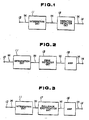
- a signal processing system generally comprises an integration circuit 11 and an amplitude detector circuit 12.
- the integrator circuit 11 is connected to an input terminal 13 which is connected to a signal source (not shown).
- the signal source supplies a constant amplitude and variable period of rectangular pulse train signal, in which each component pulse has a period variable for representing a data to indicate.
- the rectangular pulse train signal Vin(Va) is input to the integration circuit 11 via the input terminal 13.
- the integration circuit 11 continuously or periodically integrate the signal level of each component pulse of the rectangular pulse train signal to produce a triangular signal Vb.
- an amplitude of the triangular signal Vb represented by a difference between the positive peak level and the negative peak level is proportional of the period of the component pulses of the rectangular pulse train signal.
- the amplitude detector circuit 12 generates a direct current signal Vc having a signal level corresponding to the amplitude of the triangular signal Vb.
- the amplitude detector circuit 12 outputs the direct current signal Vc via an output terminal 14.
- the level of the triangular signal Vb vaires since the level of the triangular signal Vb vaires generally in linear fashion without causing abrupt change of the signal level. No noise will be created.
- Fig. 2 is a block diagram of the first embodiment of the signal processing system for practically implementing the present invention.
- the amplitude detector circuit 12 comprises a peak detector circuit 15 and an amplifier 16.
- the peak detector circuit 15 detects the peak level of the triangular signal Vb in order to output a peak signal Vd having a signal level corresponding to the detected peak level of the triangular signal Vb.
- the amplifier 16 receives the peak signal Vd to remove lipple component contained in the peak signal and produces the direct current signal having a signal level corresponding to the peak signal level.
- the amplitude detector circuit 12 comprises a full-wave rectification circuit 17 and the amplifier 16.
- the full-wave rectification circuit 17 outputs positive polarity triangular signal having amplitude corresponding top half of the triangular signal Vb.
- the amplifier 16 receives the full-wave rectified triangular signal to produce the direct current signal Vc having a signal level representative of the period of the component pulse.
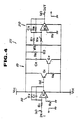
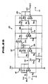
- Fig. 4 is a circuit of first implementation of the first embodiment of the signal processing system according to the present invention.
- the shown circuit comprises an integrator circuit 18, a peak detector circuit 19 and an amplifier circuit 20.
- the integration circuit 18 comprises an operational amplifier IC1, a capacitor C1 and resistors R1, R2 and R3.
- the operational amplifier IC1 can comprise a general purpose operational amplifer.
- the capacitor C1 and resistors R1 and R2 are for setting integration constant.
- the resistor R3 serves as a bias resistor for improving in-phase voltage removal ratio (CMRR.
- the peak detector circuit 19 comprises an NPN type transistor Q1, a PNP type transistor Q2, a capacitor C2 and resistors R4 and R5.
- the NPN type transistor Q1 and the PNP type transistor Q2 are provided complementary characteristics.
- the capacitor C2 serves for detecting the peak level of the triangular signal from the integrator circuit 18.
- the resistor R4 serves as a bias resistor and the resistor R5 serves as an output resistor.
- the amplifer circuit 20 comprises an operational amplifier IC2, a capacitor C3, a variable resistors R6 and VR1 and resistors R7, R8 and R9.
- the operational amplifier IC2 comprises a general purpose operational amplifier.
- the capacitor C3 serves for absorbing lipple component.
- the variable resistor R6 and the resistor R8 define amplification degree.
- the resistor R7 and the variable resistor VR1 serves for adjusting offset.
- the resistor R9 is provided to serve as a bias resistor for improving an in-phase voltage removal ratio (CMRR).
- CMRR in-phase voltage removal ratio
- the capacitor C3, the resistor R6 and R8 are cooperated to form a low-pass filter.
- the integrator circuit 18, the peak detector circuit 19 and the amplifier 20 is connected to a positive direct current source V CC and a negative direct source V EE .
- a rectangular pulse train source which can generate a rectangular pulse train including pulse component having constant amplitude and variable period.
- such rectangular pulse train generator comprises a displacement gauge disposed between a vehicle body and a suspension member supporting a road wheel in an automotive use.
- the displacement gauge includes a crystal oscillator circuit responsive to relative and physical displacement between the vehicle body and the suspension member to produce a periodic signal in a form of constant amplitude and variable period rectangular pulse train.
- the operation of the aforementioned circuit of Fig. 4 will be discussed herebelow in terms of period-to-voltage conversion for such periodic signal of the displacement gauge.
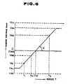
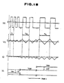
- Figs. 5 and 6 respectively showing timing chart of the operation of the signal processing system of Fig. 4 and a period-to-voltage conversion characteristics.
- the periodic signal has variable pulse period which represents relative distance between the vehicle body and the suspension member.
- the periodic signal is a rectangular pulse train having pulse component which carries signal level between a positive constant level and a negative constant level in one pulse cycle.
- the duty ratio of the positive constant level period and the negative constant level period is set at 50%.
- the period of pulse components vaires between T1, T2 and T3.
- the rectangular pulse train signal Va as the periodic signal is supplied to the inverting input terminal of the operation amplifier IC1 via an input terminal IN and the resistor R1.
- the operational amplifier IC1 forms a Miller intergrator together with the resistor R1 and the capacitor C1.
- the rectangular pulse train signal Va is integrated in the Miller integrator.
- the integrated output of the Miller integrator becomes a form of triangular wave symmetric in positive and negative phases with respect to the ground level GND.
- the direct current gain G1 of the operational amplifier IC1 is determined by the resistance of the resistors R1 and R2 according to the following equation (1).
- G1 - (R2/R1) (1)
- the level of the triangular signal Vb can be derived through the following equation (2).
- Vb - (1/(R1 x C1)) x ⁇ Vadt (2)
- the signal level of the triangular signal Vb decreases at a constant rate.
- the signal level of the triangular signal Vb increases at a constant rate.
- the amplitude of the triangular signal Vb becomes proportional to the length of the pulse period of respective pulse component.
- the peak detector circuit 19 is designed to detect the peak level of the triangular signal Vb and generate a negative level direct current signal Vd removing the lipple component.
- the triangular signal Vb is supplied to the base electrode of the NPN type transistor Q1.
- the collector of the transistor Q1 is connected to the positive power source V CC and the emitter electrode is connected to the negative power source V EE via a resistor R4.
- a junction between the emitter electrode of the transistor Q1 and the resistor R4 is connected to the base electrode of the PNP type transistor Q2.
- the transistor Q2 has the emitter electrode connected to the positive power sources V CC via a capacitor C2 and the collector electrode connected to the negative power source V EE .
- the NPN transistor Q1 is constantly maintained ON state.
- the NPN transistor Q1 has a base-emitter voltage drop V BE1 . Therefore, the potential at a junction E between the emitter electrode and the resistor R4R becomes Vb - V BE1 .
- the potential at the junction E is supplied to the PNP transistor Q2 which has a base-emitter voltage drop V BE2 .
- the transistor Q2 is maintained ON while the signal level of the triangular signal Vb is decreasing. By this a circuit between the positive power source V CC and the negative power source V EE via the capacitor C2 is established to charge the negative potential.
- the transistors Q1 and Q2 are provided complementary characteristics, the voltage drops V BE1 and V BE2 are equal to each other. Therefore, in the foregoing equation (4), the terms of voltage drops V BE1 and V BE2 are canceled. Therefore, the potential Vd at a junction F between the emitter electrode of the PNP transistor Q2 and the capacitor C2 thus becomes equal to the output level Vb.
- the triangular signal level Vb reaches the negative peak and thus turns to increase the signal level
- the base-emitter voltage drop V BE2 cannot be maintained to turn the PNP transistor Q2 OFF. Therefore, the capacitor C2 is not further charged to maintain the negative level charge level corresponding to the negative peak level of the triangular signal.
- the negative charge in the capacitor C2 is discharged through the resistor R5. Therefore, the charge level at a point C is gradually increased to reduce the negative level, as shown in Fig. 5(c).
- the capacity of the capacitor and resistance of the resistor R5 is selected to provide a predetermined time constant so that the negative peak level of the subsequent next pulse component.
- the resistor R4 serves for controlling the base current in the base electrode of the PNP transistor Q2 so that excessive collector current can be prevented. Therefore, by appropriately selecting the resistance of the resistor R4, the PNP transistor Q2 is protected from malfunctioning.
- the direct current signal Vd is supplied to an inverting input terminal of the operational amplifier IC2 via the variable resistor R6.
- the operational amplifier IC2 the direct current signal Vd is inverted and amplified. Therefore, the direct current form signal Vc which varies in alternative direction to the direction of variation of the direct current signal Vd, is output from the operational amplifier IC2, as shown in Fig. 5(d).
- the operational amplifier IC2 is provided an amplifier gain G2 which is determined by resistances of the resistors R6 and R8.
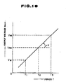
- the characteristics of the direct current signal Vc as a period-to-voltage conversion ouptut signal V out can be controlled by setting resistances of the variable resistors R6 and VR1 and the resistor R7.
- the resistors R6 and R8 and the capacitor C3 form the low-pass filter for removing lipple component.
- the shown circuit construction has NPN transistor Q1 and PNP transistor Q2 arranged in complementary characteristics, temperature dependent variation of characteristics can be successfully canceled. Furthermore, by the operation of the bias resistor R4, excess current to flow on the collector electrode of the PNP transistor Q2 can be prevented.
- the shown embodiment permits variation of output characteristics by appropriately selecting resistance of the variable resistors R6 and VR1 and the resistor R7, range of application of the shown construction of the signal processing system can be substantially widened. Furthermore, because of the effect as the low-pass filter which is implemented by the combination of the resistors R6 and R7 and the capacitor C3, suppression of lipple component in and linear characteristics of the ouput signal can be obtained.
- circuit can be fabricated in an integrated circuit so that it can be incorporated in the displacement gauge without occupying a substantial space.
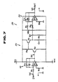
- Figs. 7 through 9 show the second implementation of the first embodiment of the signal processing system according to the invention.
- the peak detector circuit 31 is modified from the former embodiment in order to detect the positive peak level of the triangular signal Vb.
- the peak detector circuit 31 has the PNP transistor Q2 directly connected to the operational amplifier IC1 of the triangular signal generator circuit 18 which is of identical construction to the former embodiment.
- the peak detector circuit 31 also has the NPN transistor Q1 connected to a junction G between the emitter electrode of the PNP transistor Q2 and the resistor R4. Even in this arrangement, the complementary characteristics of base-emitter voltage drop of the transistors Q2 and Q1 can be established.
- the offset voltage in amplifier circuit 20 is modified to provide the characteristics of Fig. 9 by modifying the setting of the variable resistor VR1 and the resistor R7.
- a signal level of at a junction H between the emitter electrode of the NPN transistor Q1 and the capacitor C1 substantially corresponds to the signal level of the triangular signal Vb generated by the triangular signal generator circuit 18.
- the PNP transistor Q2 is normally or constantly maintained in ON state to supply the signal having a level (Vb + V BE2 ) to the NPN transistor Q2.
- the NPN transistor Q1 is maintained ON state while the signal level of the triangular signal is increasing.
- the capacitor C2 is charged by the power supplied from the positive power source V CC until the charged potential reaches the level corresponding to the positive peak level of the triangular signal.
- the triangular signal level decreases, the NPN transistor Q1 is maintained OFF to disconnect the capacitor C2 from the positive power source V CC .
- the potential charged in the capacitor C2 is gradually discharged through the resistor R5 to lower the positive signal level as shown in Fig. 8(c).
- the direct current signal Vd output from the peak detector circuit 31 is supplied to the amplifier circuit 20.
- the amplifier circuit 20 then output the direct current form voltage signal Vc as shown in Fig. 8(d).
- Figs. 10 and 11 shows the third implementation of the first embodiment of the signal processing system according to the invention.
- the shown embodiment is practically the modification of the foregoing embodiment of Figs. 4 through 6.
- the power is supplied only from the positive power source V CC . Therefore, the negative power source V EE in the former embodiment is replaced with the ground level GND.
- the shown embodiment is thus applicable for the rectangular pulse train which varies the signal level between a predetermined positive level and the ground level.
- resistors R10 and R11 are inserted between the positive power source V CC and the ground level GND so as to supply the common voltage for the non-inverting input terminal of the operational amplifiers IC1 and IC2.
- the shown embodiment is provided a capacitor C4 which serves as by-pass capacitor for by-passing noise component to be superimposed in the common voltage. Except for the signal polarities, the operation of the circuit for performing period-to-voltage conversion is substantially the same as that performed by the circuit of Fig. 4, as shown in Fig. 11.
- Figs. 12 and 13 shows the fourth implementation of the first embodiment of the signal processing system according to the invention.
- the shown embodiment is practically a modification of the foregoing embodiment of Figs. 7 through 8 and applicable for the rectangular pulse train having signal level varying between the predetermined positive level and the ground level.
- the circuit is provided single and positive power source V CC , as shown in Fig. 12.
- the shown embodiment is provided additional resistors R10 and R11 and the by-pass capacitor C4 in the same arrangement as that in the former embodiment of Figs. 10 and 11.
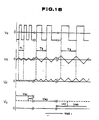
- the waveforms of the signals at respective points a, b, c and d are shown in Fig. 13.
- Figs. 14 to 16 show the first implementation of the second embodiment of the signal processing system according to the present invention.
- the shown embodiment employs the full-wave rectification circuit 32 for generating full-wave rectified negative polarity triangular signal.
- the full-wave rectification circuit 32 comprises a half-wave rectification circuit 33 and a summing amplifier 34.
- the half-wave rectification circuit 33 comprises resistors R4 and R5, a diode D2, a general purpose operational amplifer IC3.
- the diode D1 serves for preventing the operational amplifier IC3 from causing saturation of input and/or output voltage.
- the resistor R6 serves for improving CMRR of the operational amplifer IC3.
- the half-wave rectification circuit 33 further has a diode D1 which serves for preventing the operational amplifier IC3 from input/output voltage in excess of saturation voltage while the triangular signal level Vb is higher than zero.
- the summing amplifier 34 comprises resistors R7, R8 and R9 and a general purpose operational amplifer IC4.
- a resistor R10 is also provided for improving CMRR of the operational amplifier IC4.
- the triangular signal Vb of the triangular signal generator circuit 18 is supplied to the inverting input terminal of the operational amplifier IC3 via the resistor R4.
- the half-wave rectification circuit 33 generates half-wave rectified triangular signal Ve.
- the half-wave rectified triangular signal Ve is maintained zero while the triangular signal level is higher than or equal to zero and, assuming the resistances of the resistors R4 and R5 are equal to each other, varies according to variation of the triangular signal level Vb while the polarity of the triangular signal Vb is maintained negative.
- the triangular signal Vb is further supplied to the inverting input terminal of the operational amplifier IC4 via the resistor R7. Furthermore, the half-wave rectified triangular level Ve is also supplied to the invention input terminal of the operational amplifier IC4 via the resistor R8. The operational amplifier IC4 thus outputs the full-wave rectified signal Vd as shown in Fig. 15(c).
- the amplifier circuit 20 has the same construction to that in the first embodiment set forth above, and performs peak hold-operation for generating direct current form voltage signal Vc having signal level corresponding to the period of the pulse period of the rectangular pulse train.
- the amplifier circuit is provided variable output characteristics for varying output level in relation to the input level by adjusting setting of resistances of the variable resistors and associated resistors, as shown in Fig. 16.
- Figs. 17 through 19 show the second implementation of the second embodiment of the signal processing system according to the invention.
- the shown embodiment is practically derived as modification of the former embodiment of Figs. 14 through 16.
- the circuit of the second implementation is differentiated from the former embodiment at the alternation of polarities of the diodes D1 and D2.
- the polarity of the full-wave rectified signal Vc Namely, as seen from Fig. 18, the polarity of the full-wave rectified signal.
- the half-wave rectified triangular signal Ve generated by the half-wave rectification circuit 36 becomes has positive phase. Therefore, the full-wave rectified signal Vd as the output of the summing amplifier 34 becomes positive phase.
- Figs. 20 through 22 show the third implementation of the second embodiment of the signal processing system according to the invention.
- the shown embodiment is particularly applicable for the rectangular pulse train having signal level varying between the positive level and the ground level GND.
- the common voltage for respective operational amplifiers IC1, IC2, IC3 and IC4 are provided by resistors R15 and R16 which forms voltage divider for diving the positive power source voltage V CC to produce the common voltage.
- a noise by-pass capacitor C3 is also provided for removing noise component superimposing the common voltage.
- the full-wave rectification circuit 33 in the shown circuit of Fig. 20 generates negative polarity full-wave rectified signal.
- the circuit of Fig. 17 can be modified as shown in Fig. 23 as the fourth implementation of the second embodiment of the signal processing system according to the invention.
Landscapes
- Amplifiers (AREA)
- Measurement Of Current Or Voltage (AREA)
Abstract
Description
- The present invention relates generally to a signal processing system for performing period-to-voltage conversion for converting rectangular pulse train form signal into a voltage signal having a signal level variable depending upon a period of the rectangular pulses. More specifically, the invention relates to a signal processing technology for avoiding influence of noise in period-to-voltage conversion.
- In the recently automotive suspension technologies, there have been proposed various suspension control systems which can control suspension characteristics for damping and absorbing vibration energy for achieving both of riding comfort and driving stability. In order to accomplish this, it is essential to precisely monitor relative displacement between vehicle bodies and road wheels rotatably supported by means of suspension members, such as suspension arms, suspension links and so forth. Some of the sensors employed for monitoring the relative distance between the vehicle bodies and he road wheels are designed to produce signals having pulse widths variable depending upon the monitored distances. When such type of sensor is employed in a suspension control system, it becomes necessary to provide a period-to-voltage converter circuit for converting the relative distance indicative pulse period in to a voltage signal for indicating the data of relative distance by signal voltage level.
- For example, Japanese Patent First (unexamined) Publications (Tokkai) Showa 53-87276 and 56-57961 discloses signal processing system performing the period-to-voltage operation. The system disclosed in Tokkai Showa 53-87276, is provided with a wave shaping circuit for shaping input signal into a constant level rectangular pulse train. The period of each rectangular pulse is detected by a period detector circuit. The period detector circuit detects leading edge of the rectangular pulse to produce a pulse signal. A saw tooth signal generator receives the pulse signal generated by the period detector circuit ot be reset and generate a saw tooth wave signal having a peak level variable depending upon resetting interval. The saw tooth wave signal of the saw tooth signal generator is fed to a sample/hold circuit which samples the saw tooth signal and hold the saw tooth signal level at the occurrence of the reset pulse of the period detector circuit. The output of the sample/hold circuit is fed to a low-pass filter which removes a lipple contained in the sample/hold output. The low-pass filter output is fed as the period-to-voltage converted output.
- The period detector circuit normally comprises a resistor, capacitor, a diode and logic circuit. On the other hand, the saw tooth generator circuit comprises a bootstrap circuit, and the sample/hold circuit comprises an input pulse synchronization type sample/hold circuit. Such circuit construction encounters the problems set out herebelow.
- The saw tooth signal generator circuit causes abrupt voltage drop as reset by the reset pulse to cause abrupt variation of current to create noise. The noise created by the saw tooth signal generator circuit tends to be propagate to associated circuits to cause malfunction of the associated circuit components in the worst case. Furthermore, the saw tooth signal generator and the sample/hold circuit has to be accurately synchronized to each other for obtaining accurate converting operation. The clearly requires timing pulse and thus requires a clock generator which is capable of generating synchronization pulse. Such necessity of additional clock or synchronization pulse generator necessarily cause rising of the cost.
- On the other hand, Tokkai Showa 56-57961 discloses a period-to-voltage converter circuit which converts the rectangular wave form input signal into saw tooth wave signal. The saw tooth wave signal is converted into direct current signal by an averaging circuit. This circuit also has the drawback of generation of OFF-set noise which is contained in the former publication.
- Therefore, it is an object of the present invention to provide a signal processing system which can convert rectangular pulse period into a voltage signal with successful suppression of noise.
- Another object of the invention is to provide a signal processing system for performing period-to-voltage conversion with simplified circuit construction and lower cost.
- In order to accomplish aforementioned and other objects, a signal processing system, according to the present invention, employs a triangular signal generator for generating an alternating polarity of triangular signal having positive and negative peak level variable depending upon pulse period of rectangular pulse signal. A direct current voltage signal is generated to have a voltage level proportional to the amplitude of the triangular signal.
- According to one aspect of the invention, a signal processing system for converting a constant amplitude and variable period periodic signal into a voltage signal, comprises:
a triangular signal generator circuit receiving the periodic signal and converting the periodic signal into a triangular signal having an amplitude corresponding to the period of the periodic signal; and
a direct current generator circuit for receiving the triangular signal to produce a direct current voltage signal having a voltage level variable in proportion to the amplitude of the triangular signal. - The signal processing system performs period-to-voltage conversion for a rectangular pulse train. Preferably, the triangular signal generator circuit comprises an integrator circuit for integrating periodic signal to generate triangular pulse signal. On the other hand, the direct current generator circuit comprises a peak detector circuit for detecting a peak level of the triangular signal and producing a direct current signal having a signal level corresponding to the peak level of the triangular signal. The direct current generator circuit further comprises an amplifier for receiving the direct current signal from the peak detector circuit and amplifying the direct current with a predetermined output characteristics for outputting the direct current voltage signal.
- The amplifier circuit may further operates to remove lipple component supper imposing on the direct current signal of the peak detector circuit. In addition, the output characteristics is variable according to a predetermined schedule.
- The peak detector circuit may include a switching transistor having a predetermined base-emitter voltage drop and means for compensating the base emitter voltage drop. The compensating means may comprise a normally conductive transistor arranged in complementary fashion with respect to the switching transistor.
- In the alternative embodiment, the direct current generator circuit comprises a full-wave rectification circuit receiving the triangular signal and producing a full-wave rectified signal, and an amplifier circuit for amplifying the full-wave rectified signal to output the direct current voltage signal. The full-wave rectification circuit may comprise a half-wave rectification circuit and a summing amplifier. According to another aspect of the invention, a signal processing system for converting a constant amplitude and variable period periodic signal into a voltage signal, comprises:
a first converter means receiving the periodic signal and converting the periodic signal into a first converted signal having a continuous signal level increasing cycle and signal level decreasing cycle and defining an upper and lower peak levels which appearing in each cycle of the periodic signal, the upper and lower peak levels defining an amplitude of the first converted signal, which amplitude is variable corresponding to the period of the periodic signal; and
a second converter means for receiving the first converted signal and producing a direct current voltage signal having a voltage level variable in proportion to the amplitude of the triangular signal. - The present invention will be understood more fully from the detailed description given herebelow and from the accompanying drawings of the preferred embodiment of the invention, which, however, should not be taken to limit the invention to the specific embodiment but are for explanation and understanding only.
- In the drawings:
- Fig. 1 is a block diagram showing basic or fundamental idea of a signal processing system according to the present invention;
- Fig. 2 is a conceptual block diagram of the first embodiment of a signal processing system for practically implementing the present invention;
- Fig. 3 is a conceptual block diagram of the second embodiment of a signal processing system for practically implementing the present invention;
- Fig. 4 is a circuit diagram of a first practical implementation of the first embodiment of the signal processing system according to the invention;
- Fig. 5 is a timing chart showing waveforms of signals in the circuit of Fig. 4;
- Fig. 6 is a chart showing input and output of the circuit of Fig. 4;
- Fig. 7 is a circuit diagram of a second practical implementation of the first embodiment of the signal processing system according to the invention;
- Fig. 8 is a timing chart showing waveforms of signals in the circuit of Fig. 7;
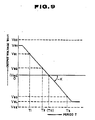
- Fig. 9 is a chart showing input and output of the circuit of Fig. 7;
- Fig. 10 is a circuit diagram of a third practical implementation of the first embodiment of the signal processing system according to the invention;
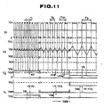
- Fig. 11 is a timing chart showing waveforms of signals in the circuit of Fig. 10;
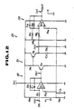
- Fig. 12 is a circuit diagram of a fourth practical implementation of the first embodiment of the signal processing system according to the invention;
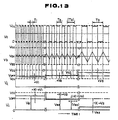
- Fig. 13 is a timing chart showing waveforms of signals in the circuit of Fig. 12;
- Fig. 14 is a circuit diagram of a first practical implementation of the second embodiment of the signal processing system according to the invention;
- Fig. 15 is a timing chart showing waveforms of signals in the circuit of Fig. 14;
- Fig. 16 is a chart showing input and output of the circuit of Fig. 4;
- Fig. 17 is a circuit diagram of a second practical implementation of the second embodiment of the signal processing system according to the invention;
- Fig. 18 is a timing chart showing waveforms of signals in the circuit of Fig. 17;
- Fig. 19 is a chart showing input and output of the circuit of Fig. 17;
- Fig. 20 is a circuit diagram of a third practical implementation of the second embodiment of the signal processing system according to the invention;
- Fig. 21 is a timing chart showing waveforms of signals in the circuit of Fig. 20;
- Fig. 22 is a chart showing input and output of the circuit of Fig. 20;
- Fig. 23 is a circuit diagram of a third practical implementation of the second embodiment of the signal processing system according to the invention;
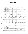
- Fig. 24 is a timing chart showing waveforms of signals in the circuit of Fig. 23 and
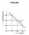
- Fig. 25 is a chart showing input and output of the circuit of Fig. 23
- Referring now to the drawings, particularly to Fig. 1, a signal processing system, according to the present invention generally comprises an integration circuit 11 and an amplitude detector circuit 12. The integrator circuit 11 is connected to an
input terminal 13 which is connected to a signal source (not shown). In the shown embodiment, the signal source supplies a constant amplitude and variable period of rectangular pulse train signal, in which each component pulse has a period variable for representing a data to indicate. The rectangular pulse train signal Vin(Va) is input to the integration circuit 11 via theinput terminal 13. The integration circuit 11 continuously or periodically integrate the signal level of each component pulse of the rectangular pulse train signal to produce a triangular signal Vb. Since the component pulses of the rectangular pulse train signal have constant amplitude, an amplitude of the triangular signal Vb represented by a difference between the positive peak level and the negative peak level is proportional of the period of the component pulses of the rectangular pulse train signal. The amplitude detector circuit 12 generates a direct current signal Vc having a signal level corresponding to the amplitude of the triangular signal Vb. The amplitude detector circuit 12 outputs the direct current signal Vc via an output terminal 14. - According to the present invention, since the level of the triangular signal Vb vaires generally in linear fashion without causing abrupt change of the signal level. No noise will be created.
- Fig. 2 is a block diagram of the first embodiment of the signal processing system for practically implementing the present invention. In this embodiment, the amplitude detector circuit 12 comprises a peak detector circuit 15 and an
amplifier 16. In the shown embodiment, the peak detector circuit 15 detects the peak level of the triangular signal Vb in order to output a peak signal Vd having a signal level corresponding to the detected peak level of the triangular signal Vb. Theamplifier 16 receives the peak signal Vd to remove lipple component contained in the peak signal and produces the direct current signal having a signal level corresponding to the peak signal level. - In the second embodiment of the signal processing system according to the invention, the amplitude detector circuit 12 comprises a full-wave rectification circuit 17 and the
amplifier 16. The full-wave rectification circuit 17 outputs positive polarity triangular signal having amplitude corresponding top half of the triangular signal Vb. Theamplifier 16 receives the full-wave rectified triangular signal to produce the direct current signal Vc having a signal level representative of the period of the component pulse. - Actual circuit constructions for implementing the aforementioned first and second embodiments of the signal processing system according to the invention will be discussed herebelow.
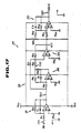
- Fig. 4 is a circuit of first implementation of the first embodiment of the signal processing system according to the present invention. The shown circuit comprises an
integrator circuit 18, apeak detector circuit 19 and anamplifier circuit 20. Theintegration circuit 18 comprises an operational amplifier IC₁, a capacitor C₁ and resistors R₁, R₂ and R₃. The operational amplifier IC₁ can comprise a general purpose operational amplifer. The capacitor C₁ and resistors R₁ and R₂ are for setting integration constant. The resistor R₃ serves as a bias resistor for improving in-phase voltage removal ratio (CMRR. - On the other hand, the
peak detector circuit 19 comprises an NPN type transistor Q₁, a PNP type transistor Q₂, a capacitor C₂ and resistors R₄ and R₅. The NPN type transistor Q₁ and the PNP type transistor Q₂ are provided complementary characteristics. The capacitor C₂ serves for detecting the peak level of the triangular signal from theintegrator circuit 18. The resistor R₄ serves as a bias resistor and the resistor R₅ serves as an output resistor. - The
amplifer circuit 20 comprises an operational amplifier IC₂, a capacitor C₃, a variable resistors R₆ and VR₁ and resistors R₇, R₈ and R₉. The operational amplifier IC₂ comprises a general purpose operational amplifier. The capacitor C₃ serves for absorbing lipple component. The variable resistor R₆ and the resistor R₈ define amplification degree. On the other hand, the resistor R₇ and the variable resistor VR₁ serves for adjusting offset. The resistor R₉ is provided to serve as a bias resistor for improving an in-phase voltage removal ratio (CMRR). In addition, the capacitor C₃, the resistor R₆ and R₈ are cooperated to form a low-pass filter. - The
integrator circuit 18, thepeak detector circuit 19 and theamplifier 20 is connected to a positive direct current source VCC and a negative direct source VEE. - To the period-to-voltage converting signal processing system of Fig. 4, a rectangular pulse train source which can generate a rectangular pulse train including pulse component having constant amplitude and variable period. For example, such rectangular pulse train generator comprises a displacement gauge disposed between a vehicle body and a suspension member supporting a road wheel in an automotive use. In this case, the displacement gauge includes a crystal oscillator circuit responsive to relative and physical displacement between the vehicle body and the suspension member to produce a periodic signal in a form of constant amplitude and variable period rectangular pulse train. The operation of the aforementioned circuit of Fig. 4 will be discussed herebelow in terms of period-to-voltage conversion for such periodic signal of the displacement gauge. In the following discussion, reference will be made for Figs. 5 and 6 which respectively showing timing chart of the operation of the signal processing system of Fig. 4 and a period-to-voltage conversion characteristics.
- As seen from Fig. 5(a), the periodic signal has variable pulse period which represents relative distance between the vehicle body and the suspension member. As seen, the periodic signal is a rectangular pulse train having pulse component which carries signal level between a positive constant level and a negative constant level in one pulse cycle. The duty ratio of the positive constant level period and the negative constant level period is set at 50%. In the shown example of Fig. 5, the period of pulse components vaires between T₁, T₂ and T₃. The rectangular pulse train signal Va as the periodic signal is supplied to the inverting input terminal of the operation amplifier IC₁ via an input terminal IN and the resistor R₁. The operational amplifier IC₁ forms a Miller intergrator together with the resistor R₁ and the capacitor C₁. The rectangular pulse train signal Va is integrated in the Miller integrator. The integrated output of the Miller integrator becomes a form of triangular wave symmetric in positive and negative phases with respect to the ground level GND. Here, the direct current gain G₁ of the operational amplifier IC₁ is determined by the resistance of the resistors R₁ and R₂ according to the following equation (1).
G₁ = - (R₂/R₁) (1)
On the other hand, the level of the triangular signal Vb can be derived through the following equation (2).
Vb = - (1/(R₁ x C₁)) x ∫Vadt (2)
Assuming that the input signal level Va is constant, the foregoing equaition (2) can be modified as:
Vb = - {Va/(R₁ x C₁)} x t + Va(0) (3)
As will be appreciated herefrom, when the input signal level Va is greater than a common voltage input at the non-inverting input terminal and serving as a reference voltage, the signal level of the triangular signal Vb decreases at a constant rate. Alternatively, when the input signal level Va is smaller than the common voltage, the signal level of the triangular signal Vb increases at a constant rate. Accrodingly, the amplitude of the triangular signal Vb becomes proportional to the length of the pulse period of respective pulse component. - The output of the operational amplifier as the triangular signal Vb is fed to the
peak detector circuit 19. In the shown embodiment, thepeak detector circuit 19 is designed to detect the peak level of the triangular signal Vb and generate a negative level direct current signal Vd removing the lipple component. For this, the triangular signal Vb is supplied to the base electrode of the NPN type transistor Q₁. The collector of the transistor Q₁ is connected to the positive power source VCC and the emitter electrode is connected to the negative power source VEE via a resistor R₄. A junction between the emitter electrode of the transistor Q₁ and the resistor R₄ is connected to the base electrode of the PNP type transistor Q₂. The transistor Q₂ has the emitter electrode connected to the positive power sources VCC via a capacitor C₂ and the collector electrode connected to the negative power source VEE. - The NPN transistor Q₁ is constantly maintained ON state. The NPN transistor Q₁ has a base-emitter voltage drop VBE1. Therefore, the potential at a junction E between the emitter electrode and the resistor R₄R becomes Vb - VBE1. The potential at the junction E is supplied to the PNP transistor Q₂ which has a base-emitter voltage drop VBE2. The transistor Q₂ is maintained ON while the signal level of the triangular signal Vb is decreasing. By this a circuit between the positive power source VCC and the negative power source VEE via the capacitor C₂ is established to charge the negative potential. The capacitor C₂ is charged at a charge level until the following equation (4) is satisfied: Vd = Vb - VBE1 + VBE2 (4)
wherein VBE2 is voltage drop between base electrode and emitter electrode of the transistor Q₂. - Because the transistors Q₁ and Q₂ are provided complementary characteristics, the voltage drops VBE1 and VBE2 are equal to each other. Therefore, in the foregoing equation (4), the terms of voltage drops VBE1 and VBE2 are canceled. Therefore, the potential Vd at a junction F between the emitter electrode of the PNP transistor Q₂ and the capacitor C₂ thus becomes equal to the output level Vb. When the triangular signal level Vb reaches the negative peak and thus turns to increase the signal level, the base-emitter voltage drop VBE2 cannot be maintained to turn the PNP transistor Q₂ OFF. Therefore, the capacitor C₂ is not further charged to maintain the negative level charge level corresponding to the negative peak level of the triangular signal. While the PNP transistor Q₂ is maintained in OFF position, the negative charge in the capacitor C₂ is discharged through the resistor R₅. Therefore, the charge level at a point C is gradually increased to reduce the negative level, as shown in Fig. 5(c). The capacity of the capacitor and resistance of the resistor R₅ is selected to provide a predetermined time constant so that the negative peak level of the subsequent next pulse component.
- It should be appreciated that, in the shown embodiment, the resistor R₄ serves for controlling the base current in the base electrode of the PNP transistor Q₂ so that excessive collector current can be prevented. Therefore, by appropriately selecting the resistance of the resistor R₄, the PNP transistor Q₂ is protected from malfunctioning.
- The direct current signal Vd representative of the negative peak level of the triangular signal Vb, which has negative level corresponding to the negative peak of the triangular signal, is output from the
peak detector circuit 19. The direct current signal Vd is supplied to an inverting input terminal of the operational amplifier IC₂ via the variable resistor R₆. By the operational amplifier IC₂, the direct current signal Vd is inverted and amplified. Therefore, the direct current form signal Vc which varies in alternative direction to the direction of variation of the direct current signal Vd, is output from the operational amplifier IC₂, as shown in Fig. 5(d). - In the shown embodiment, the operational amplifier IC₂ is provided an amplifier gain G₂ which is determined by resistances of the resistors R₆ and R₈. The gain G₂ is determined by the following equation:
G₂ = - (R₈/R₆)
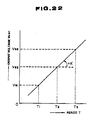
en from Fig. 5(d), the direct current signal Vd is offset by a predetermined offset voltage which is determined by the variable resistor VR₁ and the resistor R₇. Namely, as seen from Fig. 6, according to the shown embodiment, the characteristics of the direct current signal Vc as a period-to-voltage conversion ouptut signal Vout can be controlled by setting resistances of the variable resistors R₆ and VR₁ and the resistor R₇. Furthermore, the resistors R₆ and R₈ and the capacitor C₃ form the low-pass filter for removing lipple component. - As seen from Figs. 5(c) and 5(d), when the direct current signal level varies between ΔV₁, ΔV₂ and ΔV₃ with respect to the pulse period T₁, T₂ and T₃, the offset of the output signal level fromthe offset voltage can be illustrated by -kΔV₁, -kΔV₂ and -kΔV₃, wherein k is an amplification ratio. With the offset voltage, the output signal becomes Vϑ1, Vϑ2 and Vϑ3.
- With utilizing the foregoing circuit, because the saw tooth signals which are used in the prior proposed signal processing systems are not used, and replaced with a triangular signal which varies signal level gradually, noise may not be created in the system. Therefore, malfunction in the circuit components of the signal processing system can be successfully avoided. Furthermore, the shown construction of the circuit enables avoidance of a timing pulse to allow the circuit construction significantly simplified.
- Since the shown circuit construction has NPN transistor Q₁ and PNP transistor Q₂ arranged in complementary characteristics, temperature dependent variation of characteristics can be successfully canceled. Furthermore, by the operation of the bias resistor R₄, excess current to flow on the collector electrode of the PNP transistor Q₂ can be prevented.
- In addition, since the shown embodiment permits variation of output characteristics by appropriately selecting resistance of the variable resistors R₆ and VR₁ and the resistor R₇, range of application of the shown construction of the signal processing system can be substantially widened. Furthermore, because of the effect as the low-pass filter which is implemented by the combination of the resistors R₆ and R₇ and the capacitor C₃, suppression of lipple component in and linear characteristics of the ouput signal can be obtained.
- It should be noted that the foregoing circuit can be fabricated in an integrated circuit so that it can be incorporated in the displacement gauge without occupying a substantial space.
- Figs. 7 through 9 show the second implementation of the first embodiment of the signal processing system according to the invention. In this second implementation, the
peak detector circuit 31 is modified from the former embodiment in order to detect the positive peak level of the triangular signal Vb. Namely, as seen from Fig. 7, thepeak detector circuit 31 has the PNP transistor Q₂ directly connected to the operational amplifier IC₁ of the triangularsignal generator circuit 18 which is of identical construction to the former embodiment. Thepeak detector circuit 31 also has the NPN transistor Q₁ connected to a junction G between the emitter electrode of the PNP transistor Q₂ and the resistor R₄. Even in this arrangement, the complementary characteristics of base-emitter voltage drop of the transistors Q₂ and Q₁ can be established. - The offset voltage in
amplifier circuit 20 is modified to provide the characteristics of Fig. 9 by modifying the setting of the variable resistor VR₁ and the resistor R₇. - In the shown circuitry, since the complementary characteristics of base-emitter voltage drop in the PNP and NPN transistors Q₂ and Q₁, the voltage drop components can be canceled. Therefore, a signal level of at a junction H between the emitter electrode of the NPN transistor Q₁ and the capacitor C₁ substantially corresponds to the signal level of the triangular signal Vb generated by the triangular
signal generator circuit 18. - In the shown circuit arrangement, the PNP transistor Q₂ is normally or constantly maintained in ON state to supply the signal having a level (Vb + VBE2) to the NPN transistor Q₂. The NPN transistor Q₁ is maintained ON state while the signal level of the triangular signal is increasing. When the NPN transistor Q₁ is held ON, the capacitor C₂ is charged by the power supplied from the positive power source VCC until the charged potential reaches the level corresponding to the positive peak level of the triangular signal. When the triangular signal level decreases, the NPN transistor Q₁ is maintained OFF to disconnect the capacitor C₂ from the positive power source VCC. During this period, the potential charged in the capacitor C₂ is gradually discharged through the resistor R₅ to lower the positive signal level as shown in Fig. 8(c). Similarly to the former embodiment, the direct current signal Vd output from the
peak detector circuit 31 is supplied to theamplifier circuit 20. Theamplifier circuit 20 then output the direct current form voltage signal Vc as shown in Fig. 8(d). - Figs. 10 and 11 shows the third implementation of the first embodiment of the signal processing system according to the invention. The shown embodiment is practically the modification of the foregoing embodiment of Figs. 4 through 6. In the shown embodiment, the power is supplied only from the positive power source VCC. Therefore, the negative power source VEE in the former embodiment is replaced with the ground level GND. The shown embodiment is thus applicable for the rectangular pulse train which varies the signal level between a predetermined positive level and the ground level. In the shown embodiment, resistors R₁₀ and R₁₁ are inserted between the positive power source VCC and the ground level GND so as to supply the common voltage for the non-inverting input terminal of the operational amplifiers IC₁ and IC₂.
- As seen from Fig. 10, a junction I between the resistors R₁₀ and R₁₁ is connected to the non-inverted input terminals of the operational amplifiers IC₁ and IC₂ via the resistors R₃ and R₉. Therefore, the common voltages supplied to each of the operational amplifies can be illustrated by:
VCOM = {R₁₁/(R₁₀ + R₁₁)} x VCC (5)
In addition, the shown embodiment is provided a capacitor C₄ which serves as by-pass capacitor for by-passing noise component to be superimposed in the common voltage. Except for the signal polarities, the operation of the circuit for performing period-to-voltage conversion is substantially the same as that performed by the circuit of Fig. 4, as shown in Fig. 11. - Figs. 12 and 13 shows the fourth implementation of the first embodiment of the signal processing system according to the invention. The shown embodiment is practically a modification of the foregoing embodiment of Figs. 7 through 8 and applicable for the rectangular pulse train having signal level varying between the predetermined positive level and the ground level. For this, the circuit is provided single and positive power source VCC, as shown in Fig. 12. In order to provide the common voltage VCOM for the operational amplifier IC₁ and IC₂, the shown embodiment is provided additional resistors R₁₀ and R₁₁ and the by-pass capacitor C₄ in the same arrangement as that in the former embodiment of Figs. 10 and 11. The waveforms of the signals at respective points a, b, c and d are shown in Fig. 13.
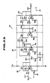
- Figs. 14 to 16 show the first implementation of the second embodiment of the signal processing system according to the present invention. The shown embodiment employs the full-
wave rectification circuit 32 for generating full-wave rectified negative polarity triangular signal. - As seen from Fig. 14, the full-
wave rectification circuit 32 comprises a half-wave rectification circuit 33 and a summingamplifier 34. The half-wave rectification circuit 33 comprises resistors R₄ and R₅, a diode D₂, a general purpose operational amplifer IC₃. The diode D₁ serves for preventing the operational amplifier IC₃ from causing saturation of input and/or output voltage. The resistor R₆ serves for improving CMRR of the operational amplifer IC₃. The half-wave rectification circuit 33 further has a diode D₁ which serves for preventing the operational amplifier IC₃ from input/output voltage in excess of saturation voltage while the triangular signal level Vb is higher than zero. On the other hand, the summingamplifier 34 comprises resistors R₇, R₈ and R₉ and a general purpose operational amplifer IC₄. A resistor R₁₀ is also provided for improving CMRR of the operational amplifier IC₄. - The triangular signal Vb of the triangular
signal generator circuit 18 is supplied to the inverting input terminal of the operational amplifier IC₃ via the resistor R₄. The half-wave rectification circuit 33 generates half-wave rectified triangular signal Ve. The half-wave rectified triangular signal Ve is maintained zero while the triangular signal level is higher than or equal to zero and, assuming the resistances of the resistors R₄ and R₅ are equal to each other, varies according to variation of the triangular signal level Vb while the polarity of the triangular signal Vb is maintained negative. - The triangular signal Vb is further supplied to the inverting input terminal of the operational amplifier IC₄ via the resistor R₇. Furthermore, the half-wave rectified triangular level Ve is also supplied to the invention input terminal of the operational amplifier IC₄ via the resistor R₈. The operational amplifier IC₄ thus outputs the full-wave rectified signal Vd as shown in Fig. 15(c). Assuming the resistance of the resistors R₇ and R₉ are equal to each other and are equal to double of the resistance of the resistor R₈, the full-wave rectified signal level Vd can be illustrated by:
Vd = - (Vb + 2Ve) (6)
Since the half-wave rectified triangular signal level is maintained zero while the triangular signal level Vb is maintained higher than or equal t zero and vaires according to variation of the triangular signal Vb while the triangular signal Vb is smaller than zero. Therefore, the following relationship between the triangular signal Vb and the full-wave rectified signal Vc is established:
when Vb ≧ 0 Vc = - Vb
Vb < 0 Vc = Vb
As will be appreciated herefrom and from Fig. 15(c), the full-wave rectified signal Vd becomes a negative polarity triangular wave signal. The amplitude of the full-wave rectified signal Vd becomes half of the amplitude of the triangular signal Vb. - In the shown embodiment, the
amplifier circuit 20 has the same construction to that in the first embodiment set forth above, and performs peak hold-operation for generating direct current form voltage signal Vc having signal level corresponding to the period of the pulse period of the rectangular pulse train. - Similarly to the foregoing first embodiment, the amplifier circuit is provided variable output characteristics for varying output level in relation to the input level by adjusting setting of resistances of the variable resistors and associated resistors, as shown in Fig. 16.
- Figs. 17 through 19 show the second implementation of the second embodiment of the signal processing system according to the invention. The shown embodiment is practically derived as modification of the former embodiment of Figs. 14 through 16. As can be seen from Fig. 17, the circuit of the second implementation is differentiated from the former embodiment at the alternation of polarities of the diodes D₁ and D₂. By the shown arrangement of the circuit, the polarity of the full-wave rectified signal Vc. Namely, as seen from Fig. 18, the polarity of the full-wave rectified signal. Namely, in the shown circuit arrangement, the half-wave rectified triangular signal Ve generated by the half-
wave rectification circuit 36 becomes has positive phase. Therefore, the full-wave rectified signal Vd as the output of the summingamplifier 34 becomes positive phase. - Figs. 20 through 22 show the third implementation of the second embodiment of the signal processing system according to the invention. The shown embodiment is particularly applicable for the rectangular pulse train having signal level varying between the positive level and the ground level GND. The common voltage for respective operational amplifiers IC₁, IC₂, IC₃ and IC₄ are provided by resistors R₁₅ and R₁₆ which forms voltage divider for diving the positive power source voltage VCC to produce the common voltage. Furthermore, a noise by-pass capacitor C₃ is also provided for removing noise component superimposing the common voltage.
- As can be seen from Fig. 21, the full-
wave rectification circuit 33 in the shown circuit of Fig. 20 generates negative polarity full-wave rectified signal. With utilizing the same arrangement for providing common voltage in Fig. 20, the circuit of Fig. 17 can be modified as shown in Fig. 23 as the fourth implementation of the second embodiment of the signal processing system according to the invention. - While the present invention has been disclosed in terms of the preferred embodiment in order to facilitate better understanding of the invention, it should be appreciated that the invention can be embodied in various ways without departing from the principle of the invention. Therefore, the invention should be understood to include all possible embodiments and modifications to the shown embodiments which can be embodied without departing from the principle of the invention set out in the appended claims.
Claims (13)
a triangular signal generator circuit receiving said periodic signal and converting said periodic signal into a triangular signal having an amplitude corresponding to the period of said periodic signal, and
a direct current generator circuit for receiving said triangular signal to produce a direct current voltage signal having a voltage level variable in proportion to said amplitude of said triangular signal.
a first converter means receiving said periodic signal and converting said periodic signal into a first converted signal having a continuous signal level increasing cycle and signal level decreasing cycle and defining an upper and lower peak levels which appearing in each cycle of said periodic signal, said upper and lower peak levels defining an amplitude of said first converted signal, which amplitude is variable corresponding to the period of said periodic signal; and
a second converter means for receiving said first converted a signal and producing a direct current voltage signal having a voltage level variable in proportion to said amplitude of said triangular signal.
Applications Claiming Priority (2)
| Application Number | Priority Date | Filing Date | Title |
|---|---|---|---|
| JP63100685A JPH01272225A (en) | 1988-04-22 | 1988-04-22 | Signal processing circuit |
| JP100685/88 | 1988-04-22 |
Publications (2)
| Publication Number | Publication Date |
|---|---|
| EP0342801A2 true EP0342801A2 (en) | 1989-11-23 |
| EP0342801A3 EP0342801A3 (en) | 1990-08-29 |
Family
ID=14280594
Family Applications (1)
| Application Number | Title | Priority Date | Filing Date |
|---|---|---|---|
| EP89304069A Withdrawn EP0342801A3 (en) | 1988-04-22 | 1989-04-24 | Signal processing system for period-to-voltage conversion |
Country Status (4)
| Country | Link |
|---|---|
| US (1) | US5049759A (en) |
| EP (1) | EP0342801A3 (en) |
| JP (1) | JPH01272225A (en) |
| AU (1) | AU611013B2 (en) |
Families Citing this family (1)
| Publication number | Priority date | Publication date | Assignee | Title |
|---|---|---|---|---|
| DE102005044801B4 (en) * | 2005-09-20 | 2013-08-01 | Zinoviy Lerner | Modulator for frequency modulation of square waves |
Citations (3)
| Publication number | Priority date | Publication date | Assignee | Title |
|---|---|---|---|---|
| US3386041A (en) * | 1965-07-26 | 1968-05-28 | Bell & Howell Co | Demodulator circuit for period modulated signals |
| JPS5387276A (en) * | 1977-01-10 | 1978-08-01 | Toshiba Corp | Pulse period-voltage converting circuit |
| DE3134630A1 (en) * | 1981-09-02 | 1983-03-10 | Robert Bosch Gmbh, 7000 Stuttgart | Electronic circuit arrangement in conjunction with a control device for internal combustion engines |
Family Cites Families (12)
| Publication number | Priority date | Publication date | Assignee | Title |
|---|---|---|---|---|
| US3336041A (en) * | 1965-09-23 | 1967-08-15 | Bouley Jean | Pushing and driving attachment for tractor |
| US3506848A (en) * | 1967-04-12 | 1970-04-14 | Henry Richard Beurrier | Pulse width to analog signal converter |
| US3535658A (en) * | 1967-06-27 | 1970-10-20 | Webb James E | Frequency to analog converter |
| US3529247A (en) * | 1967-09-20 | 1970-09-15 | Us Army | Pulse repetition to analog voltage converter |
| US3609395A (en) * | 1970-09-02 | 1971-09-28 | Ford Motor Co | Frequency to voltage converter circuit |
| JPS5352368Y2 (en) * | 1972-12-26 | 1978-12-14 | ||
| US3784845A (en) * | 1973-02-06 | 1974-01-08 | Sperry Rand Corp | Linear frequency to voltage converter circuit |
| US4160922A (en) * | 1977-08-02 | 1979-07-10 | Exxon Production Research Company | Method of generating a direct current control signal from a noisy alternating current signal |
| US4241455A (en) * | 1977-12-29 | 1980-12-23 | Sperry Corporation | Data receiving and processing circuit |
| JPS5543650A (en) * | 1978-09-25 | 1980-03-27 | Ricoh Kk | Two wire data collection system |
| US4243940A (en) * | 1978-12-07 | 1981-01-06 | Goodyear Aerospace Corporation | AC to DC converter for antiskid systems |
| JPS5657961A (en) * | 1979-10-17 | 1981-05-20 | Mitsubishi Electric Corp | Period-voltage converting circuit |
-
1988
- 1988-04-22 JP JP63100685A patent/JPH01272225A/en active Pending
-
1989
- 1989-04-21 US US07/341,358 patent/US5049759A/en not_active Expired - Fee Related
- 1989-04-24 AU AU33370/89A patent/AU611013B2/en not_active Ceased
- 1989-04-24 EP EP89304069A patent/EP0342801A3/en not_active Withdrawn
Patent Citations (3)
| Publication number | Priority date | Publication date | Assignee | Title |
|---|---|---|---|---|
| US3386041A (en) * | 1965-07-26 | 1968-05-28 | Bell & Howell Co | Demodulator circuit for period modulated signals |
| JPS5387276A (en) * | 1977-01-10 | 1978-08-01 | Toshiba Corp | Pulse period-voltage converting circuit |
| DE3134630A1 (en) * | 1981-09-02 | 1983-03-10 | Robert Bosch Gmbh, 7000 Stuttgart | Electronic circuit arrangement in conjunction with a control device for internal combustion engines |
Non-Patent Citations (4)
| Title |
|---|
| ELEKTROTECHNIK. vol. 58, no. 18, 17 September 76, WURZBURG, DE pages 25 - 26; G. HARMS: "GRUNDLAGEN UND PRAXIS DER LINEAR VERST[RKER (FOLGE: 31)" * |
| PATENT ABSTRACTS OF JAPAN vol. 2, no. 121 (E-063) 12 October 78, & JP-A-53 087276 (TOSHIBA) 01 August 78, * |
| PATENT ABSTRACTS OF JAPAN vol. 5, no. 118 (P-073) 30 July 81, & JP-A-56 057961 (MITSUBISHI) 20 May 81, * |
| U. TIETZE, CH. SCHENK: "HALBLEITER-SCHALTUNGSTECHNIK (5. Auflage)" 1980, Springer Verlag, Berlin, DE * |
Also Published As
| Publication number | Publication date |
|---|---|
| EP0342801A3 (en) | 1990-08-29 |
| US5049759A (en) | 1991-09-17 |
| AU611013B2 (en) | 1991-05-30 |
| AU3337089A (en) | 1989-11-02 |
| JPH01272225A (en) | 1989-10-31 |
Similar Documents
| Publication | Publication Date | Title |
|---|---|---|
| US6385067B2 (en) | Analog/digital PWM control circuit of a winding | |
| US4010644A (en) | Method for compensation of the electrochemical perturbing direct current potential in inductive flow measurement with a periodically switched uniform field | |
| US4987779A (en) | Pulse-driven accelerometer arrangement | |
| JPH0420238B2 (en) | ||
| JPH0615347U (en) | Data slicer | |
| US7292021B2 (en) | Anomaly detector for vibratory angular rate sensor | |
| KR0182252B1 (en) | Converter circuit | |
| JPH1090331A (en) | Surface potential sensor | |
| JPH05180661A (en) | Sensor-signal extracting circuit | |
| US6204659B1 (en) | Inductance change detection circuit | |
| MXPA00012434A (en) | Device for quick d/a conversion of pwm signals. | |
| EP0342801A2 (en) | Signal processing system for period-to-voltage conversion | |
| US4354235A (en) | Guidance system detector circuit | |
| US4868909A (en) | Signal shaping circuit utilizing a magneto-resistor in a voltage divider circuit | |
| JP3099336B2 (en) | Electromagnetic digital current detector | |
| US6345533B1 (en) | Angular rate sensor | |
| EP0184769A2 (en) | Rotational information output device | |
| EP0369011B1 (en) | Multiphase multiplier | |
| EP0377978B1 (en) | A PLL control apparatus | |
| JP3260533B2 (en) | Current detector | |
| JPH0775336B2 (en) | Optical receiver circuit | |
| EP1554850B1 (en) | Method and device for signal amplitude detection | |
| JPH09318409A (en) | Analog signal waveform shaping circuit | |
| SU1046905A1 (en) | Detector of absolute value of signal | |
| JP3052571B2 (en) | Timing pulse generation circuit in electromagnetic flowmeter |
Legal Events
| Date | Code | Title | Description |
|---|---|---|---|
| PUAI | Public reference made under article 153(3) epc to a published international application that has entered the european phase |
Free format text: ORIGINAL CODE: 0009012 |
|
| AK | Designated contracting states |
Kind code of ref document: A2 Designated state(s): DE FR GB |
|
| PUAL | Search report despatched |
Free format text: ORIGINAL CODE: 0009013 |
|
| AK | Designated contracting states |
Kind code of ref document: A3 Designated state(s): DE FR GB |
|
| 17P | Request for examination filed |
Effective date: 19910227 |
|
| STAA | Information on the status of an ep patent application or granted ep patent |
Free format text: STATUS: EXAMINATION IS IN PROGRESS |
|
| 17Q | First examination report despatched |
Effective date: 19921123 |
|
| RAP1 | Party data changed (applicant data changed or rights of an application transferred) |
Owner name: UNISIA JECS CORPORATION |
|
| 18D | Application deemed to be withdrawn |
Effective date: 19941208 |